EP0825427A2 - Resonanzstruktur und Verfahren zur Bildung der Resonanzstruktur - Google Patents
Resonanzstruktur und Verfahren zur Bildung der Resonanzstruktur Download PDFInfo
- Publication number
- EP0825427A2 EP0825427A2 EP97113020A EP97113020A EP0825427A2 EP 0825427 A2 EP0825427 A2 EP 0825427A2 EP 97113020 A EP97113020 A EP 97113020A EP 97113020 A EP97113020 A EP 97113020A EP 0825427 A2 EP0825427 A2 EP 0825427A2
- Authority
- EP
- European Patent Office
- Prior art keywords
- diaphragm
- force transducer
- recess
- resonant
- peripheral boundary
- Prior art date
- Legal status (The legal status is an assumption and is not a legal conclusion. Google has not performed a legal analysis and makes no representation as to the accuracy of the status listed.)
- Withdrawn
Links
- 238000000034 method Methods 0.000 title claims description 15
- 239000000758 substrate Substances 0.000 claims abstract description 45
- 230000002093 peripheral effect Effects 0.000 claims abstract description 35
- 230000004044 response Effects 0.000 claims abstract description 18
- 239000004065 semiconductor Substances 0.000 claims abstract description 14
- VYPSYNLAJGMNEJ-UHFFFAOYSA-N Silicium dioxide Chemical compound O=[Si]=O VYPSYNLAJGMNEJ-UHFFFAOYSA-N 0.000 claims description 58
- 239000000377 silicon dioxide Substances 0.000 claims description 30
- 239000002019 doping agent Substances 0.000 claims description 24
- 238000005530 etching Methods 0.000 claims description 21
- 239000000463 material Substances 0.000 claims description 15
- 229910021426 porous silicon Inorganic materials 0.000 claims description 15
- 238000000151 deposition Methods 0.000 claims description 11
- 229910021421 monocrystalline silicon Inorganic materials 0.000 claims description 11
- 235000012239 silicon dioxide Nutrition 0.000 claims description 11
- 239000003990 capacitor Substances 0.000 claims description 10
- 230000001590 oxidative effect Effects 0.000 claims description 10
- 238000007743 anodising Methods 0.000 claims description 2
- 229920002120 photoresistant polymer Polymers 0.000 description 31
- 229910021420 polycrystalline silicon Inorganic materials 0.000 description 20
- 229920005591 polysilicon Polymers 0.000 description 20
- 229910052681 coesite Inorganic materials 0.000 description 19
- 229910052906 cristobalite Inorganic materials 0.000 description 19
- 229910052682 stishovite Inorganic materials 0.000 description 19
- 229910052905 tridymite Inorganic materials 0.000 description 19
- 238000000137 annealing Methods 0.000 description 11
- 235000012431 wafers Nutrition 0.000 description 10
- KRHYYFGTRYWZRS-UHFFFAOYSA-N Fluorane Chemical compound F KRHYYFGTRYWZRS-UHFFFAOYSA-N 0.000 description 9
- ZOXJGFHDIHLPTG-UHFFFAOYSA-N Boron Chemical compound [B] ZOXJGFHDIHLPTG-UHFFFAOYSA-N 0.000 description 8
- XUIMIQQOPSSXEZ-UHFFFAOYSA-N Silicon Chemical compound [Si] XUIMIQQOPSSXEZ-UHFFFAOYSA-N 0.000 description 8
- 229910052796 boron Inorganic materials 0.000 description 8
- 230000008859 change Effects 0.000 description 8
- 229910052751 metal Inorganic materials 0.000 description 8
- 239000002184 metal Substances 0.000 description 8
- 238000007789 sealing Methods 0.000 description 8
- 229910052710 silicon Inorganic materials 0.000 description 8
- 239000010703 silicon Substances 0.000 description 8
- 230000008901 benefit Effects 0.000 description 7
- 238000012216 screening Methods 0.000 description 7
- 239000013078 crystal Substances 0.000 description 6
- 238000002048 anodisation reaction Methods 0.000 description 5
- 238000001465 metallisation Methods 0.000 description 5
- 229910052782 aluminium Inorganic materials 0.000 description 4
- XAGFODPZIPBFFR-UHFFFAOYSA-N aluminium Chemical compound [Al] XAGFODPZIPBFFR-UHFFFAOYSA-N 0.000 description 4
- 239000011521 glass Substances 0.000 description 4
- 238000004518 low pressure chemical vapour deposition Methods 0.000 description 4
- 238000004519 manufacturing process Methods 0.000 description 4
- 238000004377 microelectronic Methods 0.000 description 4
- 230000003647 oxidation Effects 0.000 description 4
- 238000007254 oxidation reaction Methods 0.000 description 4
- 229910052581 Si3N4 Inorganic materials 0.000 description 3
- 230000003750 conditioning effect Effects 0.000 description 3
- 230000008021 deposition Effects 0.000 description 3
- 230000037361 pathway Effects 0.000 description 3
- HQVNEWCFYHHQES-UHFFFAOYSA-N silicon nitride Chemical compound N12[Si]34N5[Si]62N3[Si]51N64 HQVNEWCFYHHQES-UHFFFAOYSA-N 0.000 description 3
- 238000005229 chemical vapour deposition Methods 0.000 description 2
- 239000004020 conductor Substances 0.000 description 2
- 238000010276 construction Methods 0.000 description 2
- 230000000694 effects Effects 0.000 description 2
- BHEPBYXIRTUNPN-UHFFFAOYSA-N hydridophosphorus(.) (triplet) Chemical group [PH] BHEPBYXIRTUNPN-UHFFFAOYSA-N 0.000 description 2
- 239000007943 implant Substances 0.000 description 2
- 238000002513 implantation Methods 0.000 description 2
- 239000011810 insulating material Substances 0.000 description 2
- 230000010355 oscillation Effects 0.000 description 2
- BASFCYQUMIYNBI-UHFFFAOYSA-N platinum Chemical compound [Pt] BASFCYQUMIYNBI-UHFFFAOYSA-N 0.000 description 2
- 230000008569 process Effects 0.000 description 2
- 230000035945 sensitivity Effects 0.000 description 2
- XLYOFNOQVPJJNP-UHFFFAOYSA-N water Substances O XLYOFNOQVPJJNP-UHFFFAOYSA-N 0.000 description 2
- XDTMQSROBMDMFD-UHFFFAOYSA-N Cyclohexane Chemical compound C1CCCCC1 XDTMQSROBMDMFD-UHFFFAOYSA-N 0.000 description 1
- 238000005275 alloying Methods 0.000 description 1
- LDDQLRUQCUTJBB-UHFFFAOYSA-N ammonium fluoride Chemical compound [NH4+].[F-] LDDQLRUQCUTJBB-UHFFFAOYSA-N 0.000 description 1
- 238000006073 displacement reaction Methods 0.000 description 1
- 239000007789 gas Substances 0.000 description 1
- 238000007496 glass forming Methods 0.000 description 1
- 229910000040 hydrogen fluoride Inorganic materials 0.000 description 1
- 239000007788 liquid Substances 0.000 description 1
- 238000013017 mechanical damping Methods 0.000 description 1
- 239000000075 oxide glass Substances 0.000 description 1
- 238000001020 plasma etching Methods 0.000 description 1
- 229910052697 platinum Inorganic materials 0.000 description 1
- 238000000859 sublimation Methods 0.000 description 1
- 230000008022 sublimation Effects 0.000 description 1
Images








Classifications
-
- G—PHYSICS
- G01—MEASURING; TESTING
- G01L—MEASURING FORCE, STRESS, TORQUE, WORK, MECHANICAL POWER, MECHANICAL EFFICIENCY, OR FLUID PRESSURE
- G01L9/00—Measuring steady of quasi-steady pressure of fluid or fluent solid material by electric or magnetic pressure-sensitive elements; Transmitting or indicating the displacement of mechanical pressure-sensitive elements, used to measure the steady or quasi-steady pressure of a fluid or fluent solid material, by electric or magnetic means
- G01L9/0041—Transmitting or indicating the displacement of flexible diaphragms
- G01L9/0042—Constructional details associated with semiconductive diaphragm sensors, e.g. etching, or constructional details of non-semiconductive diaphragms
-
- G—PHYSICS
- G01—MEASURING; TESTING
- G01L—MEASURING FORCE, STRESS, TORQUE, WORK, MECHANICAL POWER, MECHANICAL EFFICIENCY, OR FLUID PRESSURE
- G01L1/00—Measuring force or stress, in general
- G01L1/18—Measuring force or stress, in general using properties of piezo-resistive materials, i.e. materials of which the ohmic resistance varies according to changes in magnitude or direction of force applied to the material
- G01L1/183—Measuring force or stress, in general using properties of piezo-resistive materials, i.e. materials of which the ohmic resistance varies according to changes in magnitude or direction of force applied to the material by measuring variations of frequency of vibrating piezo-resistive material
-
- G—PHYSICS
- G01—MEASURING; TESTING
- G01L—MEASURING FORCE, STRESS, TORQUE, WORK, MECHANICAL POWER, MECHANICAL EFFICIENCY, OR FLUID PRESSURE
- G01L9/00—Measuring steady of quasi-steady pressure of fluid or fluent solid material by electric or magnetic pressure-sensitive elements; Transmitting or indicating the displacement of mechanical pressure-sensitive elements, used to measure the steady or quasi-steady pressure of a fluid or fluent solid material, by electric or magnetic means
- G01L9/0001—Transmitting or indicating the displacement of elastically deformable gauges by electric, electro-mechanical, magnetic or electro-magnetic means
- G01L9/0008—Transmitting or indicating the displacement of elastically deformable gauges by electric, electro-mechanical, magnetic or electro-magnetic means using vibrations
- G01L9/0019—Transmitting or indicating the displacement of elastically deformable gauges by electric, electro-mechanical, magnetic or electro-magnetic means using vibrations of a semiconductive element
-
- G—PHYSICS
- G01—MEASURING; TESTING
- G01L—MEASURING FORCE, STRESS, TORQUE, WORK, MECHANICAL POWER, MECHANICAL EFFICIENCY, OR FLUID PRESSURE
- G01L9/00—Measuring steady of quasi-steady pressure of fluid or fluent solid material by electric or magnetic pressure-sensitive elements; Transmitting or indicating the displacement of mechanical pressure-sensitive elements, used to measure the steady or quasi-steady pressure of a fluid or fluent solid material, by electric or magnetic means
- G01L9/0041—Transmitting or indicating the displacement of flexible diaphragms
- G01L9/0051—Transmitting or indicating the displacement of flexible diaphragms using variations in ohmic resistance
- G01L9/0052—Transmitting or indicating the displacement of flexible diaphragms using variations in ohmic resistance of piezoresistive elements
- G01L9/0055—Transmitting or indicating the displacement of flexible diaphragms using variations in ohmic resistance of piezoresistive elements bonded on a diaphragm
-
- G—PHYSICS
- G01—MEASURING; TESTING
- G01P—MEASURING LINEAR OR ANGULAR SPEED, ACCELERATION, DECELERATION, OR SHOCK; INDICATING PRESENCE, ABSENCE, OR DIRECTION, OF MOVEMENT
- G01P15/00—Measuring acceleration; Measuring deceleration; Measuring shock, i.e. sudden change of acceleration
- G01P15/02—Measuring acceleration; Measuring deceleration; Measuring shock, i.e. sudden change of acceleration by making use of inertia forces using solid seismic masses
- G01P15/08—Measuring acceleration; Measuring deceleration; Measuring shock, i.e. sudden change of acceleration by making use of inertia forces using solid seismic masses with conversion into electric or magnetic values
- G01P15/0802—Details
-
- G—PHYSICS
- G01—MEASURING; TESTING
- G01P—MEASURING LINEAR OR ANGULAR SPEED, ACCELERATION, DECELERATION, OR SHOCK; INDICATING PRESENCE, ABSENCE, OR DIRECTION, OF MOVEMENT
- G01P15/00—Measuring acceleration; Measuring deceleration; Measuring shock, i.e. sudden change of acceleration
- G01P15/02—Measuring acceleration; Measuring deceleration; Measuring shock, i.e. sudden change of acceleration by making use of inertia forces using solid seismic masses
- G01P15/08—Measuring acceleration; Measuring deceleration; Measuring shock, i.e. sudden change of acceleration by making use of inertia forces using solid seismic masses with conversion into electric or magnetic values
- G01P15/12—Measuring acceleration; Measuring deceleration; Measuring shock, i.e. sudden change of acceleration by making use of inertia forces using solid seismic masses with conversion into electric or magnetic values by alteration of electrical resistance
- G01P15/123—Measuring acceleration; Measuring deceleration; Measuring shock, i.e. sudden change of acceleration by making use of inertia forces using solid seismic masses with conversion into electric or magnetic values by alteration of electrical resistance by piezo-resistive elements, e.g. semiconductor strain gauges
Definitions
- the invention relates to transducers for measuring force, and particularly to a silicon microelectronic mechanical structure for measuring force.
- the invention also relates to a method of forming the microelectronic mechanical force transducer.
- semiconductor force transducers typically exhibit a low sensitivity to force.
- existing semiconductor force transducers are of limited use in measuring very low forces or very small force changes.
- known semiconductor force transducers and resonating beams are typically formed from a polysilicon material which makes connection of the electronics to the microelectronic mechanical structure difficult and expensive.
- the invention provides a force transducer including a semiconductor substrate having a surface defining a recess, such that the recess has a peripheral boundary.
- the force transducer also includes a flexible diaphragm connected to the surface along the peripheral boundary to enclose the recess so that the diaphragm moves in response to changes in a force applied thereto.
- the force transducer also includes a resonant beam connected to the surface adjacent the peripheral boundary.
- the resonant beam has a resonant frequency such that movement of the diaphragm in response to changes in the force on the diaphragm results in a change to the resonant frequency of the resonant beam.
- the flexible diaphragm or the resonant beam or both are formed from single crystal silicon.
- the invention also provides a method of forming the force transducer.
- the method includes the steps of implanting in the substrate layer a one of an n-type or p-type dopant; doping the substrate to create a first region doped with the other of the n-type or the p-type dopant, and a second region spaced from the first region and being doped with the other of the n-type or the p-type dopant; depositing an epitaxial layer on said surface over said first and second regions; implanting a first sinker through the epitaxial layer and into connection with the first regent; implanting a second sinker through the epitaxial layer and into connection with the second region; anodizing the substrate to form porous silicon of the first and second sinkers and of the first and second regions; oxidizing the porous silicon to form silicon dioxide; and etching the silicon dioxide to form the recess, the flexible diaphragm, and the resonant beam.
- Figure 1 is an enlarged perspective view of the microelectronic mechanical force transducer.
- Figure 2 is a dark field mask for use in the step of implanting an n-type buried layer in the structure forming the transducer.
- Figure 3 is a dark field mask for use in the step of doping the structure with a p-type dopant.
- Figure 4 is a top-down view of the structure after the step of doping.
- Figure 5 is a dark field mask for use in the step of implanting sinkers through the epitaxial layer.
- Figure 6 is a top-down view of the structure after the step of implanting sinkers through the epitaxial layer.
- Figure 7 is a dark field mask for use in the step of implanting the capacitor and piezoresistor.
- Figure 8 is a top-down view of the structure after the step of implanting the capacitor and piezoresistor.
- Figure 9 is a clear field mask for use in the step of creating an oxidized silicon cover over a portion of the structure.
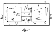
- Figure 10 is a top-down view of the structure after the step of creating an oxidized silicon cover.
- Figure 11 is a dark field mask for use in the step of creating anchor regions on the structure.
- Figure 12 is a top-down view of the structure after the step of creating anchor regions.
- Figure 13 is a clear field mask for use in the step of creating polysilicon covers at various points on the structure.
- Figure 14 is a top-down view of the structure after the step of creating polysilicon covers at various points.
- Figure 14A is a dark field mask for use in the step of creating an n-type sinker on the structure.
- Figure 14B is a dark field mask for use in the step of creating a p-type region in the cover layer.
- Figure 14C is a top-down view of the structure after the step of implanting the n-type sinker and the p-type region.
- Figure 15 is a dark field mask for use in the step of creating metalization contacts on the structure.
- Figure 16 is a top-down view of the structure after the step of creating metalization contacts.
- Figure 17 is a clear field mask for use in the step of creating conductive metal current flow pathways overlaying the metalization contacts.
- Figure 18 is a top-down view of the structure after the step of creating the conductive metal pathways.
- Figure 19 is a view taken along line 19-19 in Figure 4 before any process steps were performed on the substrate.
- Figure 20 is a view taken along line 20-20 in Figure 4 after the steps of implanting the N-type layer and doping the P-type buried regions.
- Figure 21 is a view taken along line 21-21 in Figure 6.
- Figure 22 is a view taken along line 22-22 in Figure 6.
- Figure 23 is a view taken along line 23-23 in Figure 6.
- Figure 24 is a view taken along line 24-24 in Figure 8.
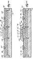
- Figure 25 is a view taken along line 25-25 in Figure 10.
- Figure 26 is a view taken along-line 26-26 in Figure 12.
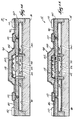
- Figure 27 is a view taken along line 27-27 in Figure 14.
- Figure 28 is a view taken along line 28-28 in Figure 14.
- Figure 29 is a view taken along line 29-29 in Figure 16.
- Figure 30 is an enlarged perspective view of a force transducer that is an another embodiment of the invention.
- Figure 31 is a dark field mask for use in the step of implanting an n-type buried layer in the structure forming the transducer of Figure 30.
- Figure 32 is a dark field mask for use in the step of doping the structure forming the transducer of Figure 30 with a p-type dopant.
- Figure 33 is a dark field mask for use in the step of implanting p-type sinkers through the epitaxial layer of the structure forming the transducer of Figure 30.
- Figure 34 is a dark field mask for use in the step of implanting the capacitor and piezoresistor in the structure forming the transducer of Figure 30.
- Figure 35 is a clear field mask for use in the step of creating an oxidized silicon cover over a portion of the structure forming the transducer of Figure 30.
- Figure 36 is a dark field mask for use in the step of creating anchor regions on the structure forming the transducer of Figure 30.
- Figure 37 is a clear field mask for use in the step of creating polysilicon covers at various points on the structure forming the transducer of Figure 30.
- Figure 38 is a dark field mask for use in the step of creating an n-type sinker on the structure forming the transducer of Figure 30.
- Figure 39 is a dark field mask for use in the step of creating a p-type region in the cover layer of the transducer of Figure 30.
- Figure 40 is a dark field mask for use in the step of creating metalization contacts on the structure forming the transducer of Figure 30.
- Figure 41 is a clear field mask for use in the step of creating conductive metal current flow pathways overlaying the metalization contacts.
- a force transducer 10 embodying the invention.
- various types of force transducers such as pressure sensors, strain sensors and displacement sensors may be formed according to the invention, the force transducer 10 is a pressure sensor.
- the force transducer 10 is formed from a substrate 14 of single crystal silicon which is altered as set forth below in the description of the method of making the transducer 10.
- the substrate 14 is a p-type silicon wafer of lightly doped P(100) silicon having p-type boron dopant with a carrier concentration between 10 15 and 10 16 cm -3 , a ⁇ 100 ⁇ cut lattice, 6.0-18.0 ohm-cm resistance. Wafers meeting SEMI standard prime CZ or float zone, for example, are suitable.
- the substrate 14 includes a horizontal upper surface 18. Although the substrate 14 can be of any suitable thickness, in the illustrated embodiment, the substrate 14 is about 500 microns thick.
- the upper surface 18 defines an elongated cavity or recess 22 (Figs. 28 and 29) having a pair of spaced sidewall surfaces 26 (only one of which is shown in Fig. 29), a pair of spaced end wall surfaces 34 extending between the sidewall surfaces 26, and a horizontal bottom surface 42 extending between the sidewall surfaces and end wall surfaces.
- the sidewall surfaces 26, end wall surfaces 34 and bottom surface 42 thus cooperate to define the cavity 22.
- the upper surface 18 also defines two square cavities or recesses 46 and 50 adjacent respective end wall surfaces 34. More particularly, the cavities 46 and 50 include peripheral boundaries 54 and 58 adjacent the end wall surfaces 34, respectively.
- the epitaxial layer 60 is deposited on the upper surface 18.
- the epitaxial layer 60 includes a center portion forming a plate or beam 62 (best shown in Figs. 22 and 23) which extends across the cavity 22.
- the beam 62 has a longitudinal axis 66 and includes opposite end portions 70 engaging the upper surface 18 adjacent the end wall surfaces 34 so that the beam 62 is capable of resonating at a given frequency in response to a stimulus.
- the resonant plate or beam 62 may be circular or another shape and include an edge portions.
- end portions is defined to include any edge portion of the plate or beam 62, notwithstanding the actual shape of the plate or beam 62.
- the beam 62 is part of the epitaxial layer 60. In other embodiments (not shown), the beam 62 can be formed partially in the epitaxial layer 60 and in the upper surface 18 of the substrate 14. Also the beam 62 can be of any suitable length, however, in the illustrated embodiment, the length of the beam 62 is about 100 ⁇ m.
- the beam 62 includes an upper surface 72 and a lower surface 74 spaced from the bottom wall 36.
- the beam 62 has a thickness of about 1.5 microns between the upper and lower surfaces 72 and 74, respectively.
- the beam 62 also includes a pair of oppositely facing side surfaces 82 (only one of which is shown in Figs. 1 and 28) extending between the upper and lower surfaces 72 and 74.
- the side surfaces 82 are generally parallel to the side wall surfaces 26.
- the beam 62 also has a width defined by the distance between the side surfaces 82, which, in the illustrated embodiment, is about 20 microns.
- the epitaxial layer 60 includes two diaphragm portions 86 and 90 adjacent the respective end portions 70 of beam 62.
- the diaphragm portions 86 and 90 cover the square cavities 46 and 50, respectively.
- the diaphragm portions 86 and 90 each include five sealed apertures 94 (shown in the "unsealed" state in Fig. 6) formed therein. As described in greater detail below, the sealed apertures 94 facilitate fabrication of the transducer 10 and are formed and sealed during fabrication of the transducer 10.
- the diaphragm portions 86 and 90 are deflectable, either upwardly or downwardly, in response to a change in the force or pressure applied to the diaphragm portions 86 and 90. Movement of the diaphragm portions 86 and 90 changes the strain in the beam 62 and thereby changes the frequency at which the beam 62 resonates.
- the transducer 10 also includes a cover layer 98 mounted on the epitaxial layer 60.
- the cover layer 98 includes a center portion 102 spaced from the upper surface 72 of the beam 62, and a periphery 106 supporting the cover layer 98 on the epitaxial layer 60 so as to completely cover the beam 62 and seal the cavity 22.
- the cover layer 98 cooperates with the side walls 26, end walls 34 and bottom wall 42 of the upper surface 18 to enclose the cavity 22 and thus define a closed space about the beam 62 so that the beam 62 can resonate within the cavity 22.
- the cover layer 98 consists of polysilicon having a thickness of about 2 microns.
- the space between the cover layer 98 and the upper surface 72 of the beam 62 can be of any suitable dimension, in the illustrated embodiment the cover layer 98 is spaced about 1 micron above the upper surface 72 of the beam 62. As described in greater detail below, the cavity 22 is preferably evacuated to minimize mechanical damping of the resonating beam 62.
- the transducer 10 also includes covers 110 (numbered in Figs. 1, 14 and 27-29 only), which cover the apertures 94 in the diaphragm portions 86 and 90 to completely seal the cavities 46 and 50.
- covers 110 consist of polysilicon having a thickness of about 2 microns.
- the transducer 10 includes means for causing resonant motion of the beam 62.
- the means for causing resonant motion of the beam 62 includes a pair of electrodes 114 and 118 (best shown in Fig. 29) which cooperate in response to an electrical stimulus to define a capacitive drive.
- the electrodes 114 and 118 are electrically connected to circuitry (not shown) to control the capacitive drive. It will be apparent to those skilled in the art that the beam 62 is caused to vibrate or resonate by operation of the capacitive drive in a known manner. It is also apparent that various combinations of dopants can be used to form the electrodes 114 and 118.
- the transducer 10 includes means for measuring resonating motion of the beam 62.
- the means for measuring resonating motion of the beam 62 is a piezoresistor 122.
- the piezoresistor 122 is created by implanting in the beam 62, a dopant, such as boron.
- the piezoresistor 122 is connected to integrated circuitry (not shown) in manner well known to those of ordinary skill in the art.
- the resistance of the piezoresistor 122 changes with strain in the beam 62 in accordance with the piezoresistive effect, and thus permits resonance of the beam 62 to be measured in a known manner.
- the transducer 10 includes metal contacts 126 and electrical conductors 130 connected to the metal contacts 126 for providing a means of connecting the electrodes 114 and 118 and piezoresistor 122 to other circuitry (not shown).
- the metal contacts 126 are aluminum, which is deposited on the epitaxial layer 60.
- the electrical contacts may be formed by dopants implanted to define conductive regions.
- the transducer 10 having the specific construction described herein is formed by altering the p-type substrate 14 according to the following steps:
- steps regarding the n-type layer, and the p-type layers may differ if different means are employed for causing resonance of the beam 62 or for measuring the resonant frequency of the beam 62.
- the substrate 14 is prepared for implantation of the buried n-type layer 134 by initially forming a screening layer of SiO 2 on the upper surface 18 of the substrate 14.
- the screening layer of SiO 2 has a thickness of about 5000 +/- 500 angstroms.
- Oxidation to form the SiO 2 screening layer is carried out by first "pushing" with about 2.25 liters per minute (l/m) of N 2 at a temperature of about 550°C for a period of about 4 hours, ramping about 2.25 l/m of O 2 gas at a rate of about 20°C/minute, oxidizing with about 2.25 l/m of H 2 and O 2 at about 1000°C, and then ramping with about 8 l/m of N 2 at a rate of about 20°C/minute.
- the term “pushing” as used herein means inserting the wafer into the furnace.
- the term “ramping" means changing the temperature in the furnace.
- the SiO 2 screening layer is thereafter etched to achieve a substantially uniform thickness. Etching with a 10:1 buffered oxide etching solution for a period of about 5 minutes is suitable. A suitable etching solution includes about 40% ammonia fluoride, 15% hydrogen fluoride and 45% water. Those skilled in the art will recognize that forming and etching a screening layer of SiO 2 before each implant or deposition step may assist in control of the subsequent implantation or deposition step. In other embodiments, any of the screening layers of SiO 2 may be omitted.
- the buried n-type layer 134 is implanted by applying photoresist to the substrate 14 and then exposing the photoresist with the buried n-type layer mask shown in Fig. 2, removing the mask, and then dosing with a suitable n-type dopant.
- the n-type dopant is phosphorous, which is dosed at a concentration of 5 x 10 13 cm -2 at 150 KeV.
- the buried n-type layer 134 is driven to a final thickness of about 2 to 4 microns by thermal annealing.
- Thermal annealing can be carried out in any suitable manner, such as by pushing with 2.25 l/m of N 2 at 850°C for a period of about 30 minutes, ramping 2.25 l/m of O 2 at a rate of 20°C/minute, oxidizing with 2.25 l/m of N 2 at about 1100°C for a period of about 17 hours, and ramping with 8 l/m of N 2 at a rate of 20°C/minute.
- the thermal annealing conditions specifically described above are provided for illustration, and those skilled in the art will appreciate that different conditions may be used to achieve this result.
- the buried p-type layer 138 is implanted over the buried n-type layer 134 by first etching the substrate 14 for 5 minutes to remove the SiO 2 formed in the previous thermal annealing step.
- the buried p-type layer 138 is patterned by applying photoresist to the substrate 14 and exposing the photoresist with the mask shown in Fig. 3.
- the p-type dopant is boron.
- the boron is dosed at a concentration of 5 x 10 13 cm -2 at consecutive energy levels of 50, 100 and 150 KeV.
- the buried p-type layer 138 is driven by thermal annealing to a final thickness of about 1 ⁇ m.
- Thermal annealing can be carried out by pushing with 2.25 l/m of O 2 at 850°C for a period of about 30 minutes, ramping 2.25 l/m of O 2 at a rate of 20°C/minute, annealing with 2.25 l/m of N 2 at about 1000°C for a period of about 1 hour and 40 minutes, and ramping with 8 l/m of N 2 at a rate of 20°C/minute.
- the n-type epitaxial layer 60 is deposited on the entire upper surface 18 of the substrate 14 by epitaxial deposition.
- the substrate 14 the n-type epitaxial layer 60 is deposited by etching the substrate 14 to remove the SiO 2 formed in the previous thermal annealing step.
- the n-type epitaxial layer 60 is deposited in a conventional manner.
- the n-type epitaxial layer 60 has a thickness of about 2 +/- 0.2 microns and a resistivity of about 0.04 +/-0.02 ohms-cm.
- the p-type sinkers 142 are implanted in the n-type epitaxial layer 60 and into electrical connection with the p-type layer 138.
- the n-type epitaxial layer 60 is partially oxidized to form a screening layer of SiO 2 having a thickness of about 500 +/- 50 angstroms.
- the SiO 2 can be formed by first "pushing" with about 2.25 liters per minute (l/m) of H 2 and O 2 at a temperature of about 850°C for a period of about 10 minutes, and then oxidizing with about 2.25 l/m of H 2 and O 2 at about 850°C for a period of about 30 minutes.
- the p-type sinkers 142 are patterned by applying photoresist and exposing the photoresist with the mask shown in Fig. 5.
- the p-type dopant is boron dosed at a concentration of 4 x 10 14 cm -2 at an energy level of 175 KeV. After the p-type sinkers 142 are implanted, the photoresist is removed.
- the p-type layer 138 and the p-type sinkers 142 are anodized to form a pre-cavity region consisting of porous silicon.
- anodization of the p-type layer 138 and the p-type sinkers 142 is an electrochemical process which can be carried out in any suitable manner.
- anodization is carried out in an electrochemical cell containing from 10 to 50 weight percent hydrofluoric acid.
- the electrochemical cell is separated into two chambers by the substrate 14 being anodized.
- Two platinum plates serve as the anodic and cathodic electrodes.
- the back or lower side portion of the substrate 14 faces the anodic electrode and the upper side portion 16 faces the cathodic electrode.
- An anodization voltage between about 1 and 7 volts is applied across the electrodes.
- the anodization process automatically stops when the low resistance p-type layer 138 and p-type sinkers 142 are converted into porous silicon.
- the porous silicon thus defines a pre-cavity region in the area previously occupied by the p-type layer 138 and p-type sinkers 142.
- the porous silicon in the pre-cavity region is oxidized to form silicon dioxide.
- the porous silicon is oxidized by first "pushing" with about 2.25 liters per minute (l/m) of O 2 at a temperature of about 300°C for a period of about 1 hour to stabilize the porous silicon, ramping with 2.25 l/m of O 2 at 20°C/minute, and oxidizing with 2.25 l/m of H 2 and O 2 at 850°C for about 30 minutes to 1 hour, such that the oxide thickness is between about 1000-3000 angstroms.
- the maximum oxidation temperature is maintained at 850°C in order to avoid inelastic change in the resulting oxide.
- the porous silicon in the pre-cavity region is converted to silicon dioxide, and a layer of silicon dioxide having a thickness of about 1500 angstroms is incidentally formed over the entire upper surface of the n-type epitaxial layer 60.
- the p-type layer (i.e., electrode 114 and piezoresistor 122) is implanted in the n-type epitaxial layer 60 is patterned by applying photoresist and exposing the photoresist with the mask shown in Fig. 7.
- the p-type dopant is boron dosed at a concentration of 5 x 10 15 cm -2 at an energy level of 80 KeV.
- the p-type layer is annealed.
- the p-type layer is annealed by pushing with 2.25 l/m of N 2 at 850°C for a period of 10 minutes and oxidizing with 2.25 l/m of N 2 at 850°C for 30 minutes.
- a layer of sacrificial material is deposited over the entire n-type epitaxial layer 60 and pre-cavity regions and then etched to define the sacrificial layer 150.
- the sacrificial material is deposited over the n-type epitaxial layer 60.
- the sacrificial material is a low temperature oxide glass (LTO glass) having a thickness of about 1 micron.
- LTO glass is deposited in a known manner, such as by chemical vapor deposition (CVD).
- the sacrificial layer 150 can be silicon nitride or another suitable material.
- the LTO glass is patterned by applying photoresist and exposing the photoresist with the mask shown in Fig. 9.
- the LTO glass is etched and the mask is removed to leave the sacrificial layer 150.
- Etching with a 10:1 buffered oxide etching solution for a period of about 10 minutes is suitable to form the sacrificial layer 150.
- the photoresist thereafter is removed.
- the substrate 14 is prepared for receiving the cover layer 98 by forming anchor cavities 154 in a layer of anchor oxide.
- the anchor cavities 154 are formed in a layer of SiO 2 .
- a suitable layer of SiO 2 having a thickness of about 1500 angstroms can be formed by oxidizing with 2.25 l/m of H 2 and O 2 at 850°C for a period of 30 minutes.
- the anchor cavities 154 are patterned by applying photoresist and exposing the photoresist using the anchor mask shown in Fig. 11.
- the wafer is etched to form the anchor cavities 154 in the layer of SiO 2 .
- Etching with a 10:1 buffered oxide etching solution for a period of about 1.5 minutes is suitable to form the anchor cavities 154.
- the photoresist thereafter is removed.
- a layer of cover material is deposited over the entire upper side portion of the wafer and then etched to define the cover layer 98.
- the cover material is polysilicon deposited on the wafer by low pressure chemical vapor deposition (LPCVD).
- the polysilicon is suitably deposited at a temperature of about 580°C to about 650°C to a thickness of about 1 to 2 microns.
- the polysilicon thus deposited is firmly secured to the wafer by polysilicon which fills the anchor cavities 154 and thus defines integral polysilicon anchors.
- the cover layer 98 is patterned by applying photoresist and exposing the photoresist using the cover mask shown in Fig. 13.
- the polysilicon is etched to form the cover layer 98.
- Any suitable polysilicon etching technique can be used. For example, plasma etching with SF 6 is suitable to form the cover layer 98. The photoresist thereafter is removed.
- the porous silicon dioxide in the pre-cavity regions is removed or dissolved by etching to form the cavities 22, 46 and 50.
- Any suitable etchant may be employed.
- the etchant is hydrofluoric acid vapor.
- hydrofluoric acid vapor to etch the cavities 22, 46 and 50 eliminates the need to later dry the cavities 22, 46 and 50.
- the hydrofluoric acid vapor etches away the SiO 2 between the anchors, thus forming open etch channels in the layer underneath the cover layer 98, and thereafter etches away the LTO glass forming the sacrificial layer 150 and the silicon dioxide in the pre-cavity regions.
- the cavities 22, 46 and 50 thus formed are open, in the sense that the etch channels were formed by etching in the spaces between the anchors and underneath the cover layer 98.
- the cavities 22, 46 and 50 are sealed and evacuated using any suitable method. Such methods are commonly known in the art and are specifically shown and described in U.S. Patent Nos. 4,744,863; 4,853,669; 4,897,360; 4,996,082; 5,090,254; and 5,104,693; which are incorporated herein by reference. It is preferred to evacuate the cavity 22 in order to maximize Q of the resonating beam 62 and to evacuate the cavities 22, 46 and 50 so that they are capable of deflecting in response to changes in ambient pressure. In the illustrated embodiment, the wafer is oxidized to form residual SiO 2 layers on the inner surfaces defining the cavities 22, 46 and 50 and the etch channels.
- the residual SiO 2 layers can be formed by oxidation by pushing 2.25 l/m of H 2 and O 2 at 850°C for 10 minutes and oxidizing with 2.25 l/m of H 2 and O 2 at 850°C for 30 minutes.
- the SiO 2 layers formed on the inner surfaces of the etch channels substantially closes the etch channels.
- the etch channels are further sealed by depositing sealing polysilicon which fills any openings which may remain between the SiO 2 layers.
- the sealing polysilicon is deposited at 580°C to 650°C to a final thickness of about 1200 +/-120 angstroms. Excess amounts of the deposited sealing polysilicon thereafter are etched away, leaving residual sealing polysilicon which fills and closes any openings in the SiO 2 layer.
- the sealing polysilicon can be etched in any suitable manner.
- the sealing polysilicon is isotropically plasma etched with SF 6 . The photoresist thereafter is removed.
- O 2 remaining in the cavities 22, 46 and 50 continues to react until substantially all O 2 in the cavities 22, 46 and 50 is consumed.
- the cavities 22, 46 and 50 are thus sealed and evacuated.
- the insulating layer is deposited over the cover layer 98 and the n-type epitaxial layer 60 in a suitable manner. Any suitable insulating material can be used.
- the insulating material is silicon nitride.
- the silicon nitride is deposited by low pressure chemical vapor deposition (LPCVD) at 835°C to a thickness of about 950 +/- 90 angstroms.
- LPCVD low pressure chemical vapor deposition
- the n-type sinker 158 is implanted through the n-type epitaxial layer 60 and into electrical connection with the n-type layer.
- the n-type sinker 158 is patterned by applying photoresist and exposing the photoresist with the mask shown in Fig. 14A.
- the n-type dopant is phosphorous dosed at a concentration of 5 x 10 15 cm -2 at an energy level of 80 KeV.
- Thermal annealing can be carried out in any suitable manner, such as by pushing with 2.25 l/m of N 2 at 850°C, ramping with 2.25 l/m of O 2 at a rate of 20°C/minute, annealing with 2.25 l/m of N 2 at about 1050°C for a period of about 8.5 hours, and ramping with 8 l/m of N 2 at a rate of 20°C/minute to 850°C.
- the p-type region (i.e., electrode 118) is implanted in the polysilicon cover layer 98 by applying photoresist and exposing the photoresist with the mask shown in Fig. 14B. While many different combinations and concentrations of dopant are possible, the p-type dopant of the illustrated embodiment is boron dosed at a concentration of between 5 x 10 14 cm -2 and 5 x 10 15 cm -2 at an energy level of 60-160 Kev. After the p-type region is implanted, the photoresist is removed.
- the metal contacts 126 are deposited in a suitable manner for connection to integrated circuitry (not shown).
- electrical contact cavities are etched for receiving the electrical contacts.
- the electrical contact cavities are patterned by applying photoresist and exposing the photoresist using the electrical contact cavity mask shown in Fig. 15.
- the insulating layer is etched with a 50:1 buffered oxide etching solution for a period of about 2.5 minutes to form the electrical contact cavities 235.
- the photoresist thereafter is removed.
- the electrical contacts are then deposited in the electrical contact cavities.
- the electrical contacts are aluminum.
- the aluminum is deposited to a thickness of about 7500 angstroms and etched using the mask shown in Fig. 17. Thereafter, the aluminum electrical contacts are alloyed into contact with the silicon by alloying at 450°C with 15% H 2 and 85% N 2 .
- the beam 62 is caused to resonate by operation of the capacitive drive. Because the resistance of the piezoresistor 122 changes with each movement of the beam 62, the oscillation of the beam 62 causes oscillation of the value of the resistance of the piezoresistor 122. Force exerted on the diaphragms causes stress or strain in the beam 62 in the direction of the longitudinal axis 66 of the beam 62. This stress/strain changes the frequency at which the beam 62 is resonating. The change in frequency can be detected electronically, using signal conditioning circuitry (not shown), by detecting the changing resistance of the piezoresistor. This change in frequency is indicative of the change in the force applied to the diaphragms.
- Fig. 30 illustrates a force transducer 200 that is another embodiment of the invention. Like parts are identified using like reference numerals.
- the transducer 200 includes a substrate 14 having an upper surface 18.
- the upper surface 18 defines a generally circular cavity or recess 204 having a peripheral boundary 208, and an annular cavity, recess or channel 212 surrounding the recess 204.
- the annular recess 212 has inner and outer peripheral boundaries 216 and 220, respectively, with the peripheral boundary 208 adjacent the peripheral boundary 216.
- the transducer 200 includes an epitaxial layer 60 formed on the upper surface 18 so as to define a resonant plate or beam 224 over the recess 204 and a flexible diaphragm 226 over the recess 212.
- the plate 224 includes a center portion 228, a lower surface 232 facing the upper surface 18 of the substrate over the region of the recess 204, and an upper surface 236.
- the plate 224 also includes a passageway 240 extending between the upper surface 236 and the lower surface 232.
- the diaphragm 226 includes an upper surface 244 and a lower surface 248 and eight passageways 252 (only two of which are shown in Fig. 30) extending between the upper surface 244 and the lower surface 248. Eight covers 256 (only six of which are shown in Fig. 30) are mounted on the diaphragm 226 to enclose the passageways 252, respectively. Similar to the operation of the transducer 10, movement of the diaphragm 226 in response to a change in the force on the diaphragm 226 changes the stress or strain in the resonant plate 224, which stress or strain in turn changes the frequency at which the plate 224 resonates.
- the transducer 200 also includes a cover layer 260 mounted on the epitaxial layer 60.
- the cover layer 260 completely encloses and seals the plate 224 within an evacuated cavity 264, which cavity 264 includes the recess 204.
- the transducer 200 also includes means for causing resonant motion of the beam 224.
- the means for causing resonant motion of the beam includes a pair of electrodes 168 and 172 Electrode 168 is formed using the mask shown in Fig. 31, electrode 170 is formed using the mask shown in Fig. 34, and electrode 172 is formed using the mask shown in Fig. 39. Electrodes 168, 170 and 172 cooperate in response to an electrical stimulus to define a capacitive drive. The electrodes 168, 170 and 172 are electrically connected to circuitry (not shown) to control the capacitive drive.
- the beam 224 is caused to vibrate or resonate by operation of the capacitive drive in a known manner. In other embodiments, such as that shown in Fig. 1, it is possible to cause resonance of the beam using only two capacitor plates. It is also apparent that various combinations of dopants can be used to form the electrodes 168, 170 and 172.
- the transducer 200 includes means for measuring resonating motion of the beam 224.
- the means for measuring resonating motion of the beam 224 is a piezoresistor 176.
- the piezoresistor 176 is created by using the mask shown in Fig. 34 to implant in the beam 224, a dopant, such as boron.
- the piezoresistor 176 is connected to integrated circuitry (not shown) in manner well known to those of ordinary skill in the art.
- the resistance of the piezoresistor 176 changes with strain in the beam 224 in accordance with the piezoresistive effect, and thus permits resonance of the beam 224 to be measured in a known manner.
- the transducer 200 is formed using the same process steps used to form the transducer 10. However, instead of using the masks shown in Figs. 2, 3, 5, 7, 9, 11, 13, 14A, 14B, 15, and 17, the transducer 200 is formed using the masks shown in Figs. 31-41, respectively.
- Figs. 31-41 include reference or alignment blocks 180 for use in aligning the masks shown in Figs. 31-41 with respect to one another.
Landscapes
- Physics & Mathematics (AREA)
- General Physics & Mathematics (AREA)
- Chemical & Material Sciences (AREA)
- Analytical Chemistry (AREA)
- Measuring Fluid Pressure (AREA)
- Pressure Sensors (AREA)
Applications Claiming Priority (4)
| Application Number | Priority Date | Filing Date | Title |
|---|---|---|---|
| US2381996P | 1996-08-12 | 1996-08-12 | |
| US23819P | 1996-08-12 | ||
| US807968 | 1997-02-28 | ||
| US08/807,968 US6021675A (en) | 1995-06-07 | 1997-02-28 | Resonating structure and method for forming the resonating structure |
Publications (2)
| Publication Number | Publication Date |
|---|---|
| EP0825427A2 true EP0825427A2 (de) | 1998-02-25 |
| EP0825427A3 EP0825427A3 (de) | 2000-01-12 |
Family
ID=26697653
Family Applications (1)
| Application Number | Title | Priority Date | Filing Date |
|---|---|---|---|
| EP97113020A Withdrawn EP0825427A3 (de) | 1996-08-12 | 1997-07-29 | Resonanzstruktur und Verfahren zur Bildung der Resonanzstruktur |
Country Status (4)
| Country | Link |
|---|---|
| US (1) | US6021675A (de) |
| EP (1) | EP0825427A3 (de) |
| JP (1) | JPH1093112A (de) |
| CA (1) | CA2211678A1 (de) |
Cited By (3)
| Publication number | Priority date | Publication date | Assignee | Title |
|---|---|---|---|---|
| EP0828346A2 (de) * | 1996-08-29 | 1998-03-11 | Harris Corporation | Einkapselung durch Verbindung einer Abdeckungshalbleiterscheibe und Mikrobearbeitung |
| WO2003022732A3 (de) * | 2001-09-12 | 2003-09-04 | Infineon Technologies Ag | Verfahren zur herstellung einer membran |
| EP1584105A4 (de) * | 2002-12-13 | 2011-06-22 | Ic Mechanics Inc | Verkapselung mikroelektromechanischer (mems) vorrichtungen mittels säulengestützer abdeckkappen |
Families Citing this family (21)
| Publication number | Priority date | Publication date | Assignee | Title |
|---|---|---|---|---|
| US6407441B1 (en) * | 1997-12-29 | 2002-06-18 | Texas Instruments Incorporated | Integrated circuit and method of using porous silicon to achieve component isolation in radio frequency applications |
| US6887391B1 (en) | 2000-03-24 | 2005-05-03 | Analog Devices, Inc. | Fabrication and controlled release of structures using etch-stop trenches |
| US6800988B1 (en) * | 2000-07-11 | 2004-10-05 | Technion Research & Development Foundation Ltd. | Voltage and light induced strains in porous crystalline materials and uses thereof |
| US7083997B2 (en) * | 2000-08-03 | 2006-08-01 | Analog Devices, Inc. | Bonded wafer optical MEMS process |
| US6448103B1 (en) | 2001-05-30 | 2002-09-10 | Stmicroelectronics, Inc. | Method for making an accurate miniature semiconductor resonator |
| US6583031B2 (en) | 2001-07-25 | 2003-06-24 | Onix Microsystems, Inc. | Method of making a MEMS element having perpendicular portion formed from substrate |
| US6813412B2 (en) * | 2001-07-24 | 2004-11-02 | Michael J. Daneman | Mems element having perpendicular portion formed from substrate |
| US7906359B2 (en) * | 2002-12-03 | 2011-03-15 | Analog Devices, Inc. | Method of forming a surface micromachined MEMS device |
| US20040104444A1 (en) * | 2002-12-03 | 2004-06-03 | Wachtmann Bruce K | MEMS device with alternative electrical connections |
| US6964894B2 (en) * | 2003-06-23 | 2005-11-15 | Analog Devices, Inc. | Apparatus and method of forming a device layer |
| DE60320391D1 (de) * | 2003-07-04 | 2008-05-29 | St Microelectronics Srl | Herstellungsverfahren für eine Halbleitervorrichtung mit einem hängenden Mikrosystem und entsprechende Vorrichtung |
| US20050181572A1 (en) * | 2004-02-13 | 2005-08-18 | Verhoeven Tracy B. | Method for acoustically isolating an acoustic resonator from a substrate |
| CN101069075B (zh) * | 2004-12-08 | 2012-05-30 | Abb专利有限公司 | 制造测量变换器的方法 |
| KR100692593B1 (ko) * | 2005-01-24 | 2007-03-13 | 삼성전자주식회사 | Mems 구조체, 외팔보 형태의 mems 구조체 및밀봉된 유체채널의 제조 방법. |
| US7490519B2 (en) * | 2005-09-30 | 2009-02-17 | General Electric Company | System and method for sensing differential pressure |
| WO2010111601A2 (en) * | 2009-03-26 | 2010-09-30 | Semprius, Inc. | Methods of forming printable integrated circuit devices and devices formed thereby |
| CN105628264B (zh) * | 2016-03-23 | 2018-01-26 | 吉林大学 | 基于同步共振的高灵敏度压电压阻电容叠加力敏传感器 |
| CN108507709B (zh) * | 2018-03-14 | 2020-01-03 | 合肥工业大学 | 一种谐振式压力传感器的制备方法 |
| CN111579426B (zh) * | 2020-04-24 | 2021-04-20 | 西安交通大学 | 一种高品质因子压电悬臂梁密度传感器芯片及其工作方法和制备方法 |
| CN114354024B (zh) * | 2022-03-17 | 2022-06-07 | 成都凯天电子股份有限公司 | 高灵敏度模态耦合型硅谐振压力传感器及其压力计算方法 |
| CN116539211B (zh) * | 2023-05-06 | 2025-01-24 | 中国科学院空天信息创新研究院 | 基于梁膜敏感和体压缩敏感的谐振式高压传感器 |
Family Cites Families (53)
| Publication number | Priority date | Publication date | Assignee | Title |
|---|---|---|---|---|
| US3994009A (en) * | 1973-02-12 | 1976-11-23 | Honeywell Inc. | Stress sensor diaphragms over recessed substrates |
| US3909924A (en) * | 1974-03-27 | 1975-10-07 | Nat Semiconductor Corp | Method of fabrication of silicon pressure transducer sensor units |
| US4035823A (en) * | 1975-10-06 | 1977-07-12 | Honeywell Inc. | Stress sensor apparatus |
| GB1601547A (en) * | 1977-05-30 | 1981-10-28 | Yokogawa Electric Works Ltd | Force detector |
| GB2121953B (en) * | 1982-06-10 | 1985-09-04 | Itt Ind Ltd | Improvements in transducers |
| JPS60111129A (ja) * | 1983-11-21 | 1985-06-17 | Yokogawa Hokushin Electric Corp | 圧力センサ |
| US4532700A (en) * | 1984-04-27 | 1985-08-06 | International Business Machines Corporation | Method of manufacturing semiconductor structures having an oxidized porous silicon isolation layer |
| US5000817A (en) * | 1984-10-24 | 1991-03-19 | Aine Harry E | Batch method of making miniature structures assembled in wafer form |
| US4628591A (en) * | 1984-10-31 | 1986-12-16 | Texas Instruments Incorporated | Method for obtaining full oxide isolation of epitaxial islands in silicon utilizing selective oxidation of porous silicon |
| US4665610A (en) * | 1985-04-22 | 1987-05-19 | Stanford University | Method of making a semiconductor transducer having multiple level diaphragm structure |
| US4853669A (en) * | 1985-04-26 | 1989-08-01 | Wisconsin Alumni Research Foundation | Sealed cavity semiconductor pressure transducers and method of producing the same |
| US4744863A (en) * | 1985-04-26 | 1988-05-17 | Wisconsin Alumni Research Foundation | Sealed cavity semiconductor pressure transducers and method of producing the same |
| JPS6263828A (ja) * | 1985-09-06 | 1987-03-20 | Yokogawa Electric Corp | 振動式トランスジューサ |
| US4766666A (en) * | 1985-09-30 | 1988-08-30 | Kabushiki Kaisha Toyota Chuo Kenkyusho | Semiconductor pressure sensor and method of manufacturing the same |
| US4771638A (en) * | 1985-09-30 | 1988-09-20 | Kabushiki Kaisha Toyota Chuo Kenkyusho | Semiconductor pressure sensor |
| GB8530809D0 (en) * | 1985-12-13 | 1986-01-22 | Gen Electric Co Plc | Sensor |
| JPS6381867A (ja) * | 1986-09-25 | 1988-04-12 | Yokogawa Electric Corp | 半導体拡散ストレンゲ−ジ |
| US4975390A (en) * | 1986-12-18 | 1990-12-04 | Nippondenso Co. Ltd. | Method of fabricating a semiconductor pressure sensor |
| GB8701556D0 (en) * | 1987-01-24 | 1987-02-25 | Schlumberger Electronics Uk | Sensors |
| US4805456A (en) * | 1987-05-19 | 1989-02-21 | Massachusetts Institute Of Technology | Resonant accelerometer |
| US4800759A (en) * | 1987-08-31 | 1989-01-31 | Yokogawa Electric Corporation | Semiconductor pressure converter |
| US4771639A (en) * | 1987-09-02 | 1988-09-20 | Yokogawa Electric Corporation | Semiconductor pressure sensor |
| JPH01136378A (ja) * | 1987-11-24 | 1989-05-29 | Nissan Motor Co Ltd | 圧力変換装置の製造方法 |
| US4897360A (en) * | 1987-12-09 | 1990-01-30 | Wisconsin Alumni Research Foundation | Polysilicon thin film process |
| KR920007501B1 (ko) * | 1988-02-04 | 1992-09-04 | 요꼬가와덴기 가부시기가이샤 | 신호컨디셔너 |
| US4784721A (en) * | 1988-02-22 | 1988-11-15 | Honeywell Inc. | Integrated thin-film diaphragm; backside etch |
| JPH07104217B2 (ja) * | 1988-05-27 | 1995-11-13 | 横河電機株式会社 | 振動式トランスデューサとその製造方法 |
| US5110373A (en) * | 1988-09-13 | 1992-05-05 | Nanostructures, Inc. | Silicon membrane with controlled stress |
| US5009108A (en) * | 1988-09-16 | 1991-04-23 | Yokogawa Electric Corporation | Vibrating type transducer |
| US4901570A (en) * | 1988-11-21 | 1990-02-20 | General Motors Corporation | Resonant-bridge two axis microaccelerometer |
| US4893509A (en) * | 1988-12-27 | 1990-01-16 | General Motors Corporation | Method and product for fabricating a resonant-bridge microaccelerometer |
| US5095401A (en) * | 1989-01-13 | 1992-03-10 | Kopin Corporation | SOI diaphragm sensor |
| US4945769A (en) * | 1989-03-06 | 1990-08-07 | Delco Electronics Corporation | Semiconductive structure useful as a pressure sensor |
| US4993143A (en) * | 1989-03-06 | 1991-02-19 | Delco Electronics Corporation | Method of making a semiconductive structure useful as a pressure sensor |
| US4889590A (en) * | 1989-04-27 | 1989-12-26 | Motorola Inc. | Semiconductor pressure sensor means and method |
| JP2811768B2 (ja) * | 1989-07-17 | 1998-10-15 | 株式会社デンソー | 半導体式加速度センサおよびその製造方法 |
| US5090254A (en) * | 1990-04-11 | 1992-02-25 | Wisconsin Alumni Research Foundation | Polysilicon resonating beam transducers |
| US5188983A (en) * | 1990-04-11 | 1993-02-23 | Wisconsin Alumni Research Foundation | Polysilicon resonating beam transducers and method of producing the same |
| CN1018844B (zh) * | 1990-06-02 | 1992-10-28 | 中国科学院兰州化学物理研究所 | 防锈干膜润滑剂 |
| CN1027011C (zh) * | 1990-07-12 | 1994-12-14 | 涂相征 | 一种硅梁压阻加速度传感器及其制造方法 |
| US5189777A (en) * | 1990-12-07 | 1993-03-02 | Wisconsin Alumni Research Foundation | Method of producing micromachined differential pressure transducers |
| US5295395A (en) * | 1991-02-07 | 1994-03-22 | Hocker G Benjamin | Diaphragm-based-sensors |
| JPH04291953A (ja) * | 1991-03-20 | 1992-10-16 | Fujitsu Ltd | 保護回路 |
| FR2680574B1 (fr) * | 1991-08-23 | 1996-04-12 | Schlumberger Ind Sa | Microcapteur a poutre vibrante compense en temperature. |
| JPH0582806A (ja) * | 1991-09-20 | 1993-04-02 | Yokogawa Electric Corp | シリコン半導体圧力計の製造方法 |
| JPH0590615A (ja) * | 1991-09-30 | 1993-04-09 | Yokogawa Electric Corp | 振動形トランスデユサの製造方法 |
| US5275055A (en) * | 1992-08-31 | 1994-01-04 | Honeywell Inc. | Resonant gauge with microbeam driven in constant electric field |
| US5332469A (en) * | 1992-11-12 | 1994-07-26 | Ford Motor Company | Capacitive surface micromachined differential pressure sensor |
| US5427975A (en) * | 1993-05-10 | 1995-06-27 | Delco Electronics Corporation | Method of micromachining an integrated sensor on the surface of a silicon wafer |
| JPH0723539A (ja) * | 1993-07-14 | 1995-01-24 | Isuzu Ceramics Kenkyusho:Kk | 超高速磁石回転子 |
| US5376818A (en) * | 1993-12-16 | 1994-12-27 | Kulite Semiconductor Products, Inc. | Large area P-N junction devices formed from porous silicon |
| KR970010663B1 (ko) * | 1993-12-24 | 1997-06-30 | 만도기계 주식회사 | 8개의 빔을 갖는 브릿지형 실리콘 가속도센서 및 그 제조방법 |
| US5473944A (en) * | 1994-08-18 | 1995-12-12 | Kulite Semi Conductor Products, Inc. | Seam pressure sensor employing dielectically isolated resonant beams and related method of manufacture |
-
1997
- 1997-02-28 US US08/807,968 patent/US6021675A/en not_active Expired - Fee Related
- 1997-07-28 CA CA002211678A patent/CA2211678A1/en not_active Abandoned
- 1997-07-29 EP EP97113020A patent/EP0825427A3/de not_active Withdrawn
- 1997-08-12 JP JP9217832A patent/JPH1093112A/ja active Pending
Cited By (3)
| Publication number | Priority date | Publication date | Assignee | Title |
|---|---|---|---|---|
| EP0828346A2 (de) * | 1996-08-29 | 1998-03-11 | Harris Corporation | Einkapselung durch Verbindung einer Abdeckungshalbleiterscheibe und Mikrobearbeitung |
| WO2003022732A3 (de) * | 2001-09-12 | 2003-09-04 | Infineon Technologies Ag | Verfahren zur herstellung einer membran |
| EP1584105A4 (de) * | 2002-12-13 | 2011-06-22 | Ic Mechanics Inc | Verkapselung mikroelektromechanischer (mems) vorrichtungen mittels säulengestützer abdeckkappen |
Also Published As
| Publication number | Publication date |
|---|---|
| US6021675A (en) | 2000-02-08 |
| JPH1093112A (ja) | 1998-04-10 |
| EP0825427A3 (de) | 2000-01-12 |
| CA2211678A1 (en) | 1998-02-12 |
Similar Documents
| Publication | Publication Date | Title |
|---|---|---|
| EP0747684B1 (de) | Formen einer Siliziumstruktur in einem Hohlraum durch Anodisieren, Oxidieren und Ätzen | |
| US6021675A (en) | Resonating structure and method for forming the resonating structure | |
| US5736430A (en) | Transducer having a silicon diaphragm and method for forming same | |
| EP0400939B1 (de) | Halbleiterwandler mit Schwingelement | |
| EP1427010B1 (de) | Verfahren zur Herstellung eines Halbleitersubstrates mit mindestens einem vergrabenen Hohlraum | |
| JP5158160B2 (ja) | 振動式トランスデューサ | |
| US5352635A (en) | Silicon accelerometer fabrication method | |
| EP2599747B1 (de) | Verfahren zur Herstellung eines Resonanzwandlers | |
| US20050253209A1 (en) | Anchors for microelectromechanical systems having an SOI substrate, and method of fabricating same | |
| JP5252016B2 (ja) | 振動式トランスデューサ | |
| EP0451992A2 (de) | Schwingungserkennung eines Mikrobalkens durch eine Hülle | |
| US5604144A (en) | Method for fabricating active devices on a thin membrane structure using porous silicon or porous silicon carbide | |
| KR20010072390A (ko) | 마이크로 미케니칼 센서 및 그 제조 방법 | |
| CN1243576A (zh) | 微机械半导体装置及制造微机械半导体装置的方法 | |
| EP0890998A1 (de) | Herstellungsverfahren und integrierter piezoresistiver Drucksensor mit einem Diaphragma aus polykristallinem Halbleitermaterial | |
| JP2005037309A (ja) | 振動式トランスデューサ | |
| EP0219543B1 (de) | Halbleiterdruckwandler mit versiegeltem hohlraum und verfahren dazu | |
| US6379990B1 (en) | Method of fabricating a micromechanical semiconductor configuration | |
| US7038285B2 (en) | Very high sensitivity magnetic sensor | |
| JPH11135806A (ja) | 半導体圧力センサおよびその製造方法 | |
| JPH04304679A (ja) | 圧力センサ | |
| JP2997962B2 (ja) | 半導体センサ用単結晶半導体基板の製造方法及び半導体センサ | |
| JP3494022B2 (ja) | 半導体加速度センサの製造方法 | |
| JP2007170843A (ja) | 振動式トランスデューサおよびその製造方法 | |
| JPH0468576B2 (de) |
Legal Events
| Date | Code | Title | Description |
|---|---|---|---|
| PUAI | Public reference made under article 153(3) epc to a published international application that has entered the european phase |
Free format text: ORIGINAL CODE: 0009012 |
|
| AK | Designated contracting states |
Kind code of ref document: A2 Designated state(s): DE ES FR GB IT |
|
| 17P | Request for examination filed |
Effective date: 19990504 |
|
| PUAL | Search report despatched |
Free format text: ORIGINAL CODE: 0009013 |
|
| AK | Designated contracting states |
Kind code of ref document: A3 Designated state(s): AT BE CH DE DK ES FI FR GB GR IE IT LI LU MC NL PT SE |
|
| AKX | Designation fees paid |
Free format text: DE ES FR GB IT |
|
| 17Q | First examination report despatched |
Effective date: 20010315 |
|
| STAA | Information on the status of an ep patent application or granted ep patent |
Free format text: STATUS: THE APPLICATION IS DEEMED TO BE WITHDRAWN |
|
| 18D | Application deemed to be withdrawn |
Effective date: 20010725 |