EP0825523A1 - Méthode et circuit à multiplier un multiplicand et un multiplieur par la méthode Booth en pas itératives - Google Patents
Méthode et circuit à multiplier un multiplicand et un multiplieur par la méthode Booth en pas itératives Download PDFInfo
- Publication number
- EP0825523A1 EP0825523A1 EP97111341A EP97111341A EP0825523A1 EP 0825523 A1 EP0825523 A1 EP 0825523A1 EP 97111341 A EP97111341 A EP 97111341A EP 97111341 A EP97111341 A EP 97111341A EP 0825523 A1 EP0825523 A1 EP 0825523A1
- Authority
- EP
- European Patent Office
- Prior art keywords
- multiplier
- multiplicand
- bits
- partial product
- decoding
- Prior art date
- Legal status (The legal status is an assumption and is not a legal conclusion. Google has not performed a legal analysis and makes no representation as to the accuracy of the status listed.)
- Granted
Links
Images


Classifications
-
- G—PHYSICS
- G06—COMPUTING OR CALCULATING; COUNTING
- G06F—ELECTRIC DIGITAL DATA PROCESSING
- G06F7/00—Methods or arrangements for processing data by operating upon the order or content of the data handled
- G06F7/38—Methods or arrangements for performing computations using exclusively denominational number representation, e.g. using binary, ternary, decimal representation
- G06F7/48—Methods or arrangements for performing computations using exclusively denominational number representation, e.g. using binary, ternary, decimal representation using non-contact-making devices, e.g. tube, solid state device; using unspecified devices
- G06F7/52—Multiplying; Dividing
- G06F7/523—Multiplying only
- G06F7/533—Reduction of the number of iteration steps or stages, e.g. using the Booth algorithm, log-sum, odd-even
- G06F7/5334—Reduction of the number of iteration steps or stages, e.g. using the Booth algorithm, log-sum, odd-even by using multiple bit scanning, i.e. by decoding groups of successive multiplier bits in order to select an appropriate precalculated multiple of the multiplicand as a partial product
- G06F7/5336—Reduction of the number of iteration steps or stages, e.g. using the Booth algorithm, log-sum, odd-even by using multiple bit scanning, i.e. by decoding groups of successive multiplier bits in order to select an appropriate precalculated multiple of the multiplicand as a partial product overlapped, i.e. with successive bitgroups sharing one or more bits being recoded into signed digit representation, e.g. using the Modified Booth Algorithm
- G06F7/5338—Reduction of the number of iteration steps or stages, e.g. using the Booth algorithm, log-sum, odd-even by using multiple bit scanning, i.e. by decoding groups of successive multiplier bits in order to select an appropriate precalculated multiple of the multiplicand as a partial product overlapped, i.e. with successive bitgroups sharing one or more bits being recoded into signed digit representation, e.g. using the Modified Booth Algorithm each bitgroup having two new bits, e.g. 2nd order MBA
Definitions
- a multiplication circuit is known from US Pat. No. 5,457,804 known at which the multiplication time for multiplications is shortened with double precision, whereby either either a higher value half or a lower value Half of an input word of the multiplication circuit via a multiplexer a conventional Booth decoder is fed.
- the multiplier Y and the multiplicand X are given by their two's complement representation.
- Control signals are generated in accordance with the coding regulations of Table 1, namely the factor signal C, the shift signal K 0 and the sign signal S i .
- the control signals control the specific sequence of the individual cycles of multiplication.
- 2 shows a block diagram of a conventional Booth multiplier architecture.
- the multiplicand X is first loaded into the register REGX and the accumulation register ACCU is set to 0 and initialized.
- the individual partial products are mixed in n / 2 steps. Equation 6 generated. To do this, the multiplicand X must be multiplied by 0, 1 or 2 in each iteration.
- the sliding unit SHE1 is used for this in FIG. 2.
- the multiplication by the factor 2 means that a left shift operation of the multiplicand by one bit position must be carried out.
- the partial product PP is calculated in each iteration with the aid of a shift unit SHE2, which divides the partial product of the previous iteration by 4 (shift to the right by two bit positions). After n / 2 iterations, the product is available in the ACCU accumulation register.
- the multiplicand X must have a doubled MSB so that no overflow can occur during the execution of the additions or subtractions. With the aid of the multiplier according to FIG. 2, the equations given in Table 1 under the heading "Operation" are thus implemented.
- the factor signal C is used to pass the multiplicand X to the shift unit SHE1 or to set 0.
- Such an operation is required according to the first and last lines of Table 1.
- Multiplication by 2 is required for multiplicand X according to Table 1 in the 4th and 5th rows.
- the addition or subtraction takes place in an arithmetic logic unit ALU as a function of the sign signal S i .
- the last column of Table 1 shows when the multiplicand X has to be added or subtracted from the previous partial product PP i + 2 .
- the partial product PP i + 2 is in the accumulation register ACCU and is multiplied by 0.25 in the sliding unit SHE2 and then fed back to the ALU to form the next partial product PP i .
- the assignment of the multiplier bits y i-1 , y i , y i + 1 to the individual operations can be found in Table 1.
- the aim of the invention is the Booth algorithm explained above to modify to simplify the multiplier to reach. This goal is according to the characteristics of claim 1 solved.
- Another task is to use a booth multiplier specify the after the changed Booth algorithm is working.
- the task is to create a decoding circuit specify the control signals for the multiplier be generated.
- the block diagram according to FIG. 3 shows in comparison to the block diagram 2 that none in the left branch of the ALU Sliding unit SHE is more available. In this left branch is only a multiplication by 0 or 1 and a sign reversal carried out. But this is in the accumulator loop (right ALU branch) a variable right shift operation executed.
- the rest of the multiplier structure 3 corresponds to that of the multiplier according to Fig. 2.
- the multiplicand X is stored in the register REGX. This is either passed or set to 0 via the unit MULT, which is controlled by the factor signal C.
- the factor signal C is generated from the multiplier signal Y in a circuit C-ERZ in accordance with the operations in Table 1.
- the multiplier Y also becomes that Sign signal S i is generated in the circuit S-ERZ.
- the partial product is shifted in the SHE3 sliding unit, with multiplication by 1/2, 1/4 or 1/8 being carried out by shifting to the right in accordance with the operations to be carried out.
- Table 2 shows a possible coding of the multiplier Y. As can be seen from Table 2, an expansion of the decoding size to 5 bits is necessary, as is also described in [3].
- the value of the control signals K 1 and K 2 and the corresponding multiplication of the sliding unit SHE3 can also be found in Table 3.
- the bit y i represents the current position.
- the bits y n , y n + 1 and y n + 2 are initially set to 0 (see FIG. 4) and if the word length n is odd, one becomes Additional bit generated by doubling the multiplier MSB's.
- the multiplication is similar to the modified Booth algorithm with a constant shift vector (Fig. 2).
- First the multiplicand is loaded into the register REGX and the accumulation register ACCU is initialized. Starting at the LSB side, the 5-bit wide decoding window is placed over the two least significant bits of the multiplier Y (see FIG. 4) and shifted to the left by 2 bit positions after each iteration. The result of the decoding determines the concrete execution of the operations during an iteration.
- the partial product PP i is calculated with the help of the variable shift unit SHE3, which allows right shifts by 1, 2 or 3 bit positions. After n / 2 iterations, the product is available in the ACCU accumulation register.
- the multiplicand X must have a double MSB so that no overflow can occur during the execution of the additions or subtractions.
- Table 2 The correctness of Table 2 can be checked using Table 1.
- a multiplication by 2 is realized by an additional right shift operation of the partial product by one bit position.
- Table 2 shows the 5 bits of the multiplier Y, which are detected by the decoding window, also the factor signal C and the sign signal S, and the results of the links H 1 and H 2 or K 1 and K 2 .
- the control signals K 1 and K 2 are shown framed when the control signal K 2 is binary 1.
- Table 3 extracts the different cases from Table 2 and specifies which multiplication is to be carried out in the sliding unit SHE3. If both the control signal K 1 and K 2 are binary 1, then multiplication by 1/8 takes place by three shift operations to the right.
- control signal K 1 is binary 1 and the control signal K 2 is binary 0, then only a shift operation or a multiplication by 1/2 takes place. If the control signal K 1 is binary 0 and the control signal K 2 is binary 1, then two shift operations or a multiplication by 1/4 take place.
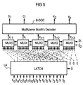
- Fig. 5 shows the block diagram of the Booth decoding circuit DEKOY with variable shift vector.
- the multiplier Y is stored with the aid of the takeover signal Ü in an n-bit latch LA.
- the decoding window function is formed using 5 multiplexers MUX1 to MUX5, each with 8 inputs. The inputs are selected one after the other by the control lines S1 to S8.
- the control signals S i , C, K 1 and K 2 are generated from the 5 bits of the current decoding window using the actual Booth decoder B-DOC in accordance with equations 7 to 12.
- FIG. 6 shows the block diagram of the Booth decoder B-DOC. Since the logical functions H 1 and H 2 are identical, they can, as shown in FIG. 6, be combined into one function by storing the results from the previous cycle. The result of the function H 1 is stored in the register REG with the takeover signal CL and corresponds to the result of the function H 2 in the next clock period. At the beginning of Booth decoding, the register content must be set to logic 0. Since the function H 2 was the only one that required the signals y i + 2 and y i + 3 , the multiplexers MUX1 and MUX2 in FIG. 5 can be dispensed with.
Landscapes
- Physics & Mathematics (AREA)
- General Physics & Mathematics (AREA)
- Engineering & Computer Science (AREA)
- Computational Mathematics (AREA)
- Mathematical Analysis (AREA)
- Mathematical Optimization (AREA)
- Pure & Applied Mathematics (AREA)
- Theoretical Computer Science (AREA)
- Computing Systems (AREA)
- General Engineering & Computer Science (AREA)
- Complex Calculations (AREA)
Applications Claiming Priority (2)
| Application Number | Priority Date | Filing Date | Title |
|---|---|---|---|
| DE19632246 | 1996-08-09 | ||
| DE19632246A DE19632246C1 (de) | 1996-08-09 | 1996-08-09 | Verfahren für eine Multiplikationsschaltung zur Multiplikation eines Multiplikanden und eines Multiplikators nach dem Booth-Verfahren in iterativen Schritten |
Publications (2)
| Publication Number | Publication Date |
|---|---|
| EP0825523A1 true EP0825523A1 (fr) | 1998-02-25 |
| EP0825523B1 EP0825523B1 (fr) | 2004-06-02 |
Family
ID=7802278
Family Applications (1)
| Application Number | Title | Priority Date | Filing Date |
|---|---|---|---|
| EP97111341A Expired - Lifetime EP0825523B1 (fr) | 1996-08-09 | 1997-07-04 | Méthode et circuit à multiplier un multiplicand et un multiplieur par la méthode Booth en pas itératives |
Country Status (3)
| Country | Link |
|---|---|
| US (1) | US5941942A (fr) |
| EP (1) | EP0825523B1 (fr) |
| DE (2) | DE19632246C1 (fr) |
Families Citing this family (3)
| Publication number | Priority date | Publication date | Assignee | Title |
|---|---|---|---|---|
| US6684236B1 (en) * | 2000-02-15 | 2004-01-27 | Conexant Systems, Inc. | System of and method for efficiently performing computations through extended booth encoding of the operands thereto |
| US20030088407A1 (en) * | 2001-04-02 | 2003-05-08 | Yi Hu | Codec |
| US8082699B1 (en) * | 2009-01-22 | 2011-12-27 | Kychelhahn Jerry A | Modular structure |
Citations (1)
| Publication number | Priority date | Publication date | Assignee | Title |
|---|---|---|---|---|
| EP0144568A2 (fr) * | 1983-09-29 | 1985-06-19 | Siemens Aktiengesellschaft | Dispositif de multiplication et sa méthode d'opération |
Family Cites Families (4)
| Publication number | Priority date | Publication date | Assignee | Title |
|---|---|---|---|---|
| JPH0831025B2 (ja) * | 1986-03-29 | 1996-03-27 | 株式会社東芝 | 乗算回路 |
| JP2597736B2 (ja) * | 1990-07-17 | 1997-04-09 | 株式会社東芝 | 高速乗算器 |
| US5220525A (en) * | 1991-11-04 | 1993-06-15 | Motorola, Inc. | Recoded iterative multiplier |
| JPH0612229A (ja) * | 1992-06-10 | 1994-01-21 | Nec Corp | 乗累算回路 |
-
1996
- 1996-08-09 DE DE19632246A patent/DE19632246C1/de not_active Expired - Fee Related
-
1997
- 1997-07-04 EP EP97111341A patent/EP0825523B1/fr not_active Expired - Lifetime
- 1997-07-04 DE DE59711682T patent/DE59711682D1/de not_active Expired - Fee Related
- 1997-08-08 US US08/907,527 patent/US5941942A/en not_active Expired - Fee Related
Patent Citations (1)
| Publication number | Priority date | Publication date | Assignee | Title |
|---|---|---|---|---|
| EP0144568A2 (fr) * | 1983-09-29 | 1985-06-19 | Siemens Aktiengesellschaft | Dispositif de multiplication et sa méthode d'opération |
Non-Patent Citations (1)
| Title |
|---|
| VOS DE L., ET AL., INTERNATIONAL CONFERENCE ON ACOUSTICS, SPEECH & SIGNAL PROCESSING. ICASSP. TOKYO, APRIL 7 - 11, 1986., NEW YORK, IEEE., US, vol. CONF. 11, 7 April 1986 (1986-04-07), US, pages 2163 - 2166., XP002047972 * |
Also Published As
| Publication number | Publication date |
|---|---|
| DE19632246C1 (de) | 1997-10-23 |
| DE59711682D1 (de) | 2004-07-08 |
| EP0825523B1 (fr) | 2004-06-02 |
| US5941942A (en) | 1999-08-24 |
Similar Documents
| Publication | Publication Date | Title |
|---|---|---|
| DE69821408T2 (de) | Multiplikationsverfahren und -vorrichtung | |
| DE3854321T2 (de) | Populationszählung in Rechnersystemen. | |
| DE4302898C2 (de) | Arithmetische Recheneinheit mit Akkumulierfunktion | |
| DE2628473C3 (de) | Digitales Faltungsfilter | |
| DE60210494T2 (de) | Hochgeschwindigkeitsberechnung in einer arithmetik- und logikschaltung | |
| DE19758079A1 (de) | Verfahren und Vorrichtung zur Galoisfeld-Multiplikation | |
| DE1956209C3 (de) | Multipliziervorrichtung | |
| DE68924386T2 (de) | Verfahren und Gerät zur Radix-2**n-Division mit überlappender Quotientenbitauswahl und gleichzeitiger Rundung und Korrektur des Quotienten. | |
| DE102007014808A1 (de) | Multiplizier- und Multiplizier- und Addiereinheit | |
| DE1549477B1 (de) | Einrichtung zur schnellen akkumulation einer anzahl mehr stelliger binaerer operanden | |
| DE2946846A1 (de) | Rundungs-korrekturlogik fuer multiplizierer fuer modifizierten booth-algorithmus | |
| DE69227791T2 (de) | Booth's Multiplikationssystem zur Durchführung von A+/- X.Y | |
| DE69226110T2 (de) | Recheneinheit zum Multiplizieren langer ganzer Zahlen Modul M und R.S.A-Wandler mit einer derartigen Multiplikationsanordnung | |
| DE2221693B2 (de) | Schaltungsanordnung zur Ausführung einer Multiplikation zwischen zwei Binärzahlen | |
| DE3854608T2 (de) | Vektorrechnerschaltung, welche schnell eine Berechnung auf drei Eingangsvektoren ausführen kann. | |
| DE3852576T2 (de) | Einrichtung und Verfahren für eine erweiterte Arithmetik-Logik-Einheit zur Beschleunigung der ausgewählten Operationen. | |
| DE10357661A1 (de) | Modularer Montgomery-Multiplizierer und zugehöriges Multiplikationsverfahren | |
| DE1549508B2 (de) | Anordnung zur uebertragsberechnung mit kurzer signallaufzeit | |
| DE10219158A1 (de) | Vorrichtung und Verfahren zum Berechnen eines Ergebnisses einer modularen Multiplikation | |
| DE69032391T2 (de) | Mehrere Bit umkodierender Multiplizierer | |
| DE3447634C2 (fr) | ||
| EP0825523B1 (fr) | Méthode et circuit à multiplier un multiplicand et un multiplieur par la méthode Booth en pas itératives | |
| DE3889746T2 (de) | Zähler. | |
| DE3416536C2 (fr) | ||
| DE10050589B4 (de) | Vorrichtung und Verfahren zur Verwendung beim Durchführen einer Gleitkomma-Multiplizier-Akkumulier-Operation |
Legal Events
| Date | Code | Title | Description |
|---|---|---|---|
| PUAI | Public reference made under article 153(3) epc to a published international application that has entered the european phase |
Free format text: ORIGINAL CODE: 0009012 |
|
| AK | Designated contracting states |
Kind code of ref document: A1 Designated state(s): DE FR GB IT |
|
| AX | Request for extension of the european patent |
Free format text: AL;LT;LV;RO;SI |
|
| 17P | Request for examination filed |
Effective date: 19980406 |
|
| AKX | Designation fees paid |
Free format text: DE FR GB IT |
|
| RBV | Designated contracting states (corrected) |
Designated state(s): DE FR GB IT |
|
| RAP1 | Party data changed (applicant data changed or rights of an application transferred) |
Owner name: INFINEON TECHNOLOGIES AG |
|
| 17Q | First examination report despatched |
Effective date: 20020927 |
|
| GRAP | Despatch of communication of intention to grant a patent |
Free format text: ORIGINAL CODE: EPIDOSNIGR1 |
|
| GRAS | Grant fee paid |
Free format text: ORIGINAL CODE: EPIDOSNIGR3 |
|
| GRAA | (expected) grant |
Free format text: ORIGINAL CODE: 0009210 |
|
| AK | Designated contracting states |
Kind code of ref document: B1 Designated state(s): DE FR GB IT |
|
| PG25 | Lapsed in a contracting state [announced via postgrant information from national office to epo] |
Ref country code: GB Free format text: LAPSE BECAUSE OF FAILURE TO SUBMIT A TRANSLATION OF THE DESCRIPTION OR TO PAY THE FEE WITHIN THE PRESCRIBED TIME-LIMIT Effective date: 20040602 |
|
| REG | Reference to a national code |
Ref country code: GB Ref legal event code: FG4D Free format text: NOT ENGLISH |
|
| REF | Corresponds to: |
Ref document number: 59711682 Country of ref document: DE Date of ref document: 20040708 Kind code of ref document: P |
|
| GBV | Gb: ep patent (uk) treated as always having been void in accordance with gb section 77(7)/1977 [no translation filed] |
Effective date: 20040602 |
|
| ET | Fr: translation filed | ||
| PLBE | No opposition filed within time limit |
Free format text: ORIGINAL CODE: 0009261 |
|
| STAA | Information on the status of an ep patent application or granted ep patent |
Free format text: STATUS: NO OPPOSITION FILED WITHIN TIME LIMIT |
|
| 26N | No opposition filed |
Effective date: 20050303 |
|
| APAH | Appeal reference modified |
Free format text: ORIGINAL CODE: EPIDOSCREFNO |
|
| APAH | Appeal reference modified |
Free format text: ORIGINAL CODE: EPIDOSCREFNO |
|
| PGFP | Annual fee paid to national office [announced via postgrant information from national office to epo] |
Ref country code: FR Payment date: 20060714 Year of fee payment: 10 |
|
| PGFP | Annual fee paid to national office [announced via postgrant information from national office to epo] |
Ref country code: IT Payment date: 20060731 Year of fee payment: 10 |
|
| PGFP | Annual fee paid to national office [announced via postgrant information from national office to epo] |
Ref country code: DE Payment date: 20060912 Year of fee payment: 10 |
|
| PG25 | Lapsed in a contracting state [announced via postgrant information from national office to epo] |
Ref country code: DE Free format text: LAPSE BECAUSE OF NON-PAYMENT OF DUE FEES Effective date: 20080201 |
|
| REG | Reference to a national code |
Ref country code: FR Ref legal event code: ST Effective date: 20080331 |
|
| PG25 | Lapsed in a contracting state [announced via postgrant information from national office to epo] |
Ref country code: FR Free format text: LAPSE BECAUSE OF NON-PAYMENT OF DUE FEES Effective date: 20070731 |
|
| PG25 | Lapsed in a contracting state [announced via postgrant information from national office to epo] |
Ref country code: IT Free format text: LAPSE BECAUSE OF NON-PAYMENT OF DUE FEES Effective date: 20070704 |