EP0827151B1 - Amplificateur de détection à auto-interruption fonctionnant sur une large plage d'alimentation - Google Patents
Amplificateur de détection à auto-interruption fonctionnant sur une large plage d'alimentation Download PDFInfo
- Publication number
- EP0827151B1 EP0827151B1 EP97114945A EP97114945A EP0827151B1 EP 0827151 B1 EP0827151 B1 EP 0827151B1 EP 97114945 A EP97114945 A EP 97114945A EP 97114945 A EP97114945 A EP 97114945A EP 0827151 B1 EP0827151 B1 EP 0827151B1
- Authority
- EP
- European Patent Office
- Prior art keywords
- circuit
- sense
- amplifier
- signal
- generating
- Prior art date
- Legal status (The legal status is an assumption and is not a legal conclusion. Google has not performed a legal analysis and makes no representation as to the accuracy of the status listed.)
- Expired - Lifetime
Links
- 238000001514 detection method Methods 0.000 claims description 39
- 230000000873 masking effect Effects 0.000 claims description 14
- 230000003213 activating effect Effects 0.000 claims description 7
- 230000005540 biological transmission Effects 0.000 claims description 2
- 230000004913 activation Effects 0.000 description 28
- 238000010586 diagram Methods 0.000 description 8
- 201000008103 leukocyte adhesion deficiency 3 Diseases 0.000 description 7
- 230000003247 decreasing effect Effects 0.000 description 6
- 230000000630 rising effect Effects 0.000 description 2
- 230000007704 transition Effects 0.000 description 2
- 230000000295 complement effect Effects 0.000 description 1
- 230000001934 delay Effects 0.000 description 1
- 230000004048 modification Effects 0.000 description 1
- 238000012986 modification Methods 0.000 description 1
- 230000003068 static effect Effects 0.000 description 1
Images


Classifications
-
- G—PHYSICS
- G11—INFORMATION STORAGE
- G11C—STATIC STORES
- G11C7/00—Arrangements for writing information into, or reading information out from, a digital store
- G11C7/06—Sense amplifiers; Associated circuits, e.g. timing or triggering circuits
-
- G—PHYSICS
- G11—INFORMATION STORAGE
- G11C—STATIC STORES
- G11C7/00—Arrangements for writing information into, or reading information out from, a digital store
- G11C7/22—Read-write [R-W] timing or clocking circuits; Read-write [R-W] control signal generators or management
-
- G—PHYSICS
- G11—INFORMATION STORAGE
- G11C—STATIC STORES
- G11C7/00—Arrangements for writing information into, or reading information out from, a digital store
- G11C7/06—Sense amplifiers; Associated circuits, e.g. timing or triggering circuits
- G11C7/062—Differential amplifiers of non-latching type, e.g. comparators, long-tailed pairs
-
- G—PHYSICS
- G11—INFORMATION STORAGE
- G11C—STATIC STORES
- G11C2207/00—Indexing scheme relating to arrangements for writing information into, or reading information out from, a digital store
- G11C2207/06—Sense amplifier related aspects
- G11C2207/065—Sense amplifier drivers
Definitions
- the present invention relates to a sense amplifier, and more particularly, to a self cut-off type sense amplifier for a static random access memory (SRAM) device.
- SRAM static random access memory
- an SRAM device after a precharging operation is carried out, complementary data is read from a selected memory cell and is sensed by a sense amplifier.
- the power dissipation of SRAM devices is mainly determined by the precharging operation and the operation of the sense amplifier.
- a prior art self cut-off type sense amplifier includes an amplifier circuit for amplifying a difference in potential between first and second data lines, an amplifier circuit activating circuit for receiving a sense start signal to activate the amplifier circuit and receiving a sense end signal to deactivate the amplifier circuit, a first sense detecting circuit for determining whether or not the amplifier circuit is activated in accordance with a first output voltage thereof and generating a first sense detection signal, a second sense detecting circuit for determining whether or not the amplifier circuit is activated in accordance with a second output voltage thereof and generating a second sense detection signal, and a sense end signal generating circuit for receiving at least one of the first and second sense detection signals and generating the sense end signal when a predetermined time has passed after at least one of the first and second sense detection signals is received.
- a self cut-off type sense amplifier which includes an amplifier circuit for amplifying a difference in potential between first and second data lines, an amplifier circuit activating circuit for receiving a sense start signal to activate the amplifier circuit and receiving a sense end signal to deactivate the amplifier circuit, a first sense detecting circuit for determining whether or not the amplifier circuit is activated in accordance with a first output voltage thereof and generating a first sense detection signal, a second sense detecting circuit for determining whether or not the amplifier circuit is activated in accordance with a second output voltage thereof and generating a second sense detection signal, and a sense end signal generating circuit for receiving at least one of the first and second sense detection signals and generating the sense end signal when a predetermined time has passed after the at least one of the first and second sense detection signals is received, a masking circuit is connected between the first and second sense detecting circuits and the sense end signal generating circuit, and prohibits transmission of the first and second sense detection signals to the sense end signal generating circuit only when the first and second sense detection
- the masking circuit delays the sense end signal, so that the timing of deactivating the amplifier circuit is after the timing of establishing output data.
- reference numeral 1 designates a memory cell array including memory cells (not shown) at intersections between word lines such as WL 1 and bit line pairs such as BL 1 and BL 1 .
- an address buffer 2 receives an external address ADD and generates an internal address IADD.
- An X component of the internal address IADD is supplied to a row decoder 3 for selecting one of the word lines, and a Y component of the internal address IADD is supplied to a column decoder 4, so that a column selector 5 selects one pair of the bit line pairs.
- a column decoder 4 selects one pair of the bit line pairs.
- the internal address IADD is supplied to an address transition detection (ATD) circuit 6 for detecting a transition of the internal address IADD to generate an ATD signal ⁇ ATD .
- ATD address transition detection
- a control circuit 7 receives the ATD signal ⁇ ATD as well as an inverted signal of a write enable signal WE to generate a precharging signal ⁇ PR , a sense activation signal ⁇ S and a write activation signal ⁇ W .
- the precharging signal ⁇ PR is supplied to precharging transistors connected to the bit lines, thus precharging the bit lines.
- the sense activation signal ⁇ S is supplied as a sense start signal to a sense amplifier 8, thus activating the sense amplifier 8.
- the write activation signal ⁇ W is supplied to a write amplifier 9, thus activating the write amplifier 9.
- the precharging signal ⁇ PR is generated from the control circuit 7 in synchronization with the ATD signal ⁇ ATD , and thereafter, one memory cell is selected by the row decoder 3 and the column decoder 4 using the internal address IADD.
- the write amplifier circuit 9 is activated, so that potentials at data lines D and D are changed in accordance with input data DI, and the potentials are written into the selected memory cell.
- the precharging signal ⁇ PR is also generated from the control circuit 7 in synchronization with the ATD signal ⁇ ATD , and thereafter, one memory cell is selected by the row decoder 3 and the column decoder 4 using the internal address IADD. As a result, potentials at the data lines D and D are changed in accordance with data in the selected memory cell. In this state, since the sense activation signal ⁇ S is also generated from the control circuit 7, the sense amplifier 8 is activated, so that the potentials at the data lines D and D are amplified, thus obtaining output data DO.
- Fig. 2 which is a detailed circuit diagram of the sense amplifier of Fig. 1, two stages of amplifier circuits 81 and 82, a sense detection circuit 83, a sense end signal generating circuit 84, and an internal sense activation signal generating circuit 85 for activating and deactivating the sense amplifier circuits 81 and 82 are provided.
- the amplifier circuit 81 is of a two end type which amplifies the potentials at the data lines D and D and generates potentials at data lines DOI and DOI .
- the amplifier circuit 81 is formed by a current mirror circuit 811 for receiving the potentials at the data lines D and D , a current mirror circuit 812 for receiving the potentials at the data lines D and D, an N-channel MOS transistor 813 for turning ON and OFF the current mirror circuits 811 and 812, and a P-channel MOS transistor 814 for equalizing the potentials at the data lines D and D .
- the amplifier circuit 82 is of a single end type which amplifies the potentials at the data lines DOI and DOI and generates the output data DO.
- the amplifier circuit 82 is formed by a current mirror circuit 821 for receiving the potentials at the data lines DOI and DOI , an N-channel MOS transistor 822 for turning ON and OFF the current mirror circuit 821, and P-channel MOS transistors 823 and 824 for pulling up the potentials at the data lines DOI and DOI .
- the sense detection circuit 83 is formed by inverters 831 and 832 for receiving the potentials at the data lines DOI and DOI , respectively.
- the inverters 831 and 832 have a common threshold voltage V th which is, in this case, an operating point. If the potential of the DOI is lower than the operating point V th , the inverter 831 generates a sense detection signal N having a high potential. Similarly, if the potential of the DOI is lower than the operating point V th , the inverter 832 generates a sense detection signal N having a high potential.
- the sense end signal generating circuit 84 is formed by delay circuits 841 and 842 connected to the inverters 831 and 832, respectively, a NAND circuit 843 for receiving the sense detection signal N of the inverter 831 and the output of the delay circuit 841, and a NAND circuit 844 for receiving the output potential N of the inverter 832 and the output of the delay circuit 842. Also, a NAND circuit 845 is connected to the outputs of the NAND circuits 843 and 845, for generating a sense end signal SE.
- the sense activation signal generating circuit 85 generates an internal sense activation signal ⁇ SI . That is, the sense activation signal generating circuit 838 includes an RS flip-flop which is set by a rising edge of the sense activation signal ⁇ S and is reset by a rising edge of the sense end signal SE.
- the transistors 813 and 814 of the amplifier circuit 81 and the transistors 822, 823 and 824 of the amplifier circuit 82 are controlled by the internal sense activation signal ⁇ SI .
- the amplifiers 81 and 82 are turned ON and OFF by the internal sense activation signal ⁇ SI , so that the sense amplifier 8 is called a self-cut type sense amplifier.
- a power supply voltage V CC applied to the sense amplifier 8 is high, for example, 2.5 to 5.5V.
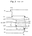
- the-sense activation signal ⁇ S is changed from low to high.
- the internal sense activation signal generating circuit 838 is set, so that the internal sense activation signal ⁇ SI rises at time t2.
- the amplifier circuits 81 and 82 are both activated.
- the amplifier circuit 81 since the current mirror circuits 811 and 812 are cross-coupled, although the potential at one of the data lines such as D remain at a high level, the potential at the other data line such as D is gradually decreased.
- the amplifier circuit 82 the potential at the data lines DOI and DOI are both gradually decreased, but the potential at one of the bit lines such as DOI is again increased.
- the NAND circuits 843, 844 and 845 in combination generate a tigger signal SE. That is, in Fig. 3, at time t3, the potential at the data line DOI becomes lower than the operating point V th , so that the sense detection signal N of the inverter 831 rises. Therefore, at time t4, when a time d corresponding to the delay time of the delay circuit 841 has passed, the sense end signal SE rises to reset the internal sense activation signal generating circuit 85, and accordingly, the internal sense activation signal ⁇ SI falls to deactivate the amplifiers 81 and 82.
- the sense activation signal ⁇ S is changed from low to high.
- the internal sense activation signal generating circuit 85 is set, so that the internal sense activation signal ⁇ SI rises at time t2.
- the amplifier circuits 81 and 82 are both activated.
- the potential at one of the data lines such as D remains at a high level, the potential at the other data line such as D is gradually decreased.
- the potentials at the data lines DOI and DOI are both gradually decreased, but the potential at one of the bit lines such as DOI is again increased.
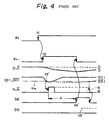
- a masking circuit 86 is interposed between the sense detection circuit 83 and the sense and signal generating circuit 84 of Fig. 2. That is, when the inverters 831 and 832 simultaneously generate the sense detection signals N and N , the masking circuit 86 disables the sense detection signal N and N, so that the sense end signal generating circuit 84 is not operated.
- the masking circuit 86 is formed by a NOR circuit 861 connected to the data lines DOI and DOI for generating a mask signal MSK.
- the NOR circuit 861 has the same operating point V th as that of the inverters 831 and 832. Therefore, only when the potentials at the data lines DOI and DOI are both lower than the operating point V th , is the mask signal MSK made high.
- the masking circuit 86 is formed by two inverters 862 and 863 connected to the inverters 831 and 832, a NOR circuit 864 connected to the NOR circuit 861 and the inverter 862, and a NOR circuit 865 connected to the NOR circuit 861 and the inverter 863.
- the sense activation signal ⁇ S is changed from low to high.
- the internal sense activation signal generating circuit 85 is set, so that the internal sense activation signal ⁇ SI rises at time t2.
- the amplifier circuits 81 and 82 are both activated.
- the potential at one of the data lines such as D remains at a high level, the potential at the other data line such as D is gradually decreased.
- the potentials at the data lines DOI and DOI are both gradually decreased, but the potential at one of the bit lines such as DOI is again increased.
- the mask signal MSK is made low.
- the sense detection signals N and N and the outputs A and A of the inverters 862 and 863 are also changed.
- the sense end signal SE rises to reset the internal sense activation signal generating circuit 85, and accordingly, the internal sense activation signal ⁇ SI falls to deactivate the amplifiers 81 and 82.
- the avove-mentioned delay time of the delay circuits 841 and 842 is about 1 to 2 ns.
- the masking circuit 86 of Fig. 5 is modified into a masking circuit 86'.
- the masking circuit 86' is formed by a NAND circuit 861', a NAND circuit 862' and an inverter 863' serving as an AND circuit, a NAND circuit 864' and an inverter 865' serving as an AND circuit, and delay circuits 866' and 867'. NOte that the delay circuits 866' and 867' have a delay time which is approximately the same as the operation time of the NAND circuit 861'. Even in Fig.
- the NAND circuit 861' when the sense detection signals N and N are both high, the NAND circuit 861' generates a mask signal MSK, so that the outputs N1 and N1 of the inverters 863' and 865' are made low regardless of the sense detection signals N and N .
- the sense amplifier 8 of Fig. 7 operates in the same way as the sense amplifier 8 of Fig. 5.
- the present invention can be applied to a sense amplifier including a single differential amplifier as illustrated in Fig. 8, where the amplifier 82 is connected directly to the data lines DO and DO .
- the timing of an output data can be sufficiently before the cut off timing of the sense amplifier.
- normal output data can be obtained.
Landscapes
- Dram (AREA)
- Static Random-Access Memory (AREA)
Claims (7)
- Amplificateur de lecture pour détecter une différence de potentiel entre des première et seconde lignes de données (D,
D ), comprenant :un circuit amplificateur (81, 82) pour amplifier ladite différence de potentiel, ledit circuit générant des première et seconde tensions de sortie (DOI,DOI ) ;un circuit d'activation de circuit amplificateur (85), connecté audit circuit amplificateur, pour recevoir un signal de début de lecture (S) afin d'activer ledit circuit amplificateur et de recevoir un signal de fin de lecture (SE) pour désactiver ledit circuit d'amplification ;un premier circuit de détection de lecture (831), connecté audit circuit amplificateur, pour déterminer si oui ou non ledit circuit amplificateur est activé en conformité avec ladite première tension de sortie et pour générer un premier signal de détection de lecture (N) ;un second circuit de détection de lecture (832), connecté audit circuit amplificateur, pour déterminer si oui ou non ledit circuit amplificateur est activé en conformité avec ladite seconde tension de sortie et générer un second signal de détection de lecture (N ) ; etun circuit générateur de signal de fin de lecture (84), connecté audit circuit d'activation de circuit amplificateur, pour recevoir au moins l'un desdits premier et second signaux de détection de lecture et générer ledit signal de fin de lecture lorsqu'un temps prédéterminé (d) s'est écoulé depuis que ledit au moins un desdits premier et second signaux de détection de lecture a été reçu, caractérisé par :un circuit de masquage (86, 86'), connecté entre lesdits premier et second circuits de détection de lecture et ledit circuit générateur de signal de fin de lecture, pour n'interdire la transmission desdits premier et second signaux de détection de lecture vers ledit circuit générateur de signal de fin de lecture, que lorsque lesdits premier et second signaux de détection de lecture sont tous deux générés. - Amplificateur de lecture selon la revendication 1, dans lequel ledit circuit de masquage comprend :un circuit NON-ET (861'), connecté auxdits premier et second circuits de détection de lecture, pour générer un signal de masquage (MSK) ;des premier et second circuits à retard (866', 867') respectivement connectés auxdits premier et second circuits de détection de lecture, et ayant un temps de retard qui est approximativement identique à un temps de fonctionnement dudit premier circuit NON-ET ;un premier circuit ET (862', 863'), connecté audit circuit NON-ET et audit premier circuit à retard, pour transmettre ledit premier signal de détection de lecture audit circuit générateur de signal de fin de lecture en conformité avec ledit signal de masquage ; etun second circuit ET (864', 865'), connecté audit circuit NON-ET et audit second circuit à retard, pour transmettre ledit second signal de détection de lecture audit circuit générateur de signal de fin de lecture en conformité avec ledit signal de masquage.
- Amplificateur de lecture selon la revendication 1, dans lequel ledit circuit de masquage (86) est en outre connecté audit circuit amplificateur.
- Amplificateur de lecture selon la revendication 3, dans lequel ledit circuit de masquage comprend :un premier circuit NON-OU (861), connecté audit circuit amplificateur, pour recevoir lesdites première et seconde tensions de sortie et générer un signal de masquage (MSK) ;un premier inverseur (862) connecté audit premier circuit de détection de lecture ;un second inverseur (862) connecté audit second circuit de détection de lecture ;un second circuit NON-OU (864), connecté audit premier circuit NON-OU et audit premier inverseur, pour transmettre ledit premier signal de détection de lecture audit circuit générateur de signal de fin de lecture en conformité avec ledit signal de masquage ; etun troisième circuit NON-OU (865), connecté audit premier circuit NON-OU et audit second inverseur, pour transmettre ledit second signal de détection de lecture audit circuit générateur de signal de fin de lecture en conformité avec ledit signal de masquage.
- Amplificateur de lecture selon la revendication 1, dans lequel ledit circuit amplificateur comprend :un premier étage amplificateur différentiel (81) pour amplifier ladite différence de potentiel et générer lesdites première et seconde tensions de sortie ; etun second étage amplificateur différentiel (82) connecté audit premier amplificateur différentiel, pour générer une différence entre lesdites première et seconde tensions de sortie.
- Amplificateur de lecture selon la revendication 1, dans lequel ledit circuit amplificateur comprend :un étage amplificateur différentiel unique (82) pour amplifier ladite différence de potentiel et générer lesdites première et seconde tensions de sortie.
- Amplificateur de lecture selon la revendication 1, dans lequel chacun des premier et second circuits de détection de lecture comprend un inverseur.
Applications Claiming Priority (3)
| Application Number | Priority Date | Filing Date | Title |
|---|---|---|---|
| JP22700496 | 1996-08-28 | ||
| JP8227004A JP2845264B2 (ja) | 1996-08-28 | 1996-08-28 | セルフカットオフ型センスアンプ回路 |
| JP227004/96 | 1996-08-28 |
Publications (2)
| Publication Number | Publication Date |
|---|---|
| EP0827151A1 EP0827151A1 (fr) | 1998-03-04 |
| EP0827151B1 true EP0827151B1 (fr) | 2002-11-27 |
Family
ID=16854009
Family Applications (1)
| Application Number | Title | Priority Date | Filing Date |
|---|---|---|---|
| EP97114945A Expired - Lifetime EP0827151B1 (fr) | 1996-08-28 | 1997-08-28 | Amplificateur de détection à auto-interruption fonctionnant sur une large plage d'alimentation |
Country Status (5)
| Country | Link |
|---|---|
| US (1) | US5872465A (fr) |
| EP (1) | EP0827151B1 (fr) |
| JP (1) | JP2845264B2 (fr) |
| KR (1) | KR100263256B1 (fr) |
| DE (1) | DE69717370D1 (fr) |
Families Citing this family (11)
| Publication number | Priority date | Publication date | Assignee | Title |
|---|---|---|---|---|
| US6025741A (en) * | 1996-12-23 | 2000-02-15 | International Business Machines Corporation | Conditional restore for execution unit |
| KR100275132B1 (ko) * | 1997-06-24 | 2000-12-15 | 김영환 | 전류미러형 감지 증폭기 |
| US6282137B1 (en) * | 1999-09-14 | 2001-08-28 | Agere Systems Guardian Corp. | SRAM method and apparatus |
| JP2001101872A (ja) | 1999-09-30 | 2001-04-13 | Mitsubishi Electric Corp | 増幅回路 |
| US6304107B1 (en) * | 2000-02-25 | 2001-10-16 | Lsi Logic Corporation | Comparator metastability performance from an enhanced comparator detection circuit |
| DE10219649C1 (de) * | 2002-05-02 | 2003-11-27 | Infineon Technologies Ag | Differentielle Strombewerterschaltung und Leseverstärkerschaltung zum Bewerten eines Speicherzustands einer SRAM-Halbleiterspeicherzelle |
| KR100483028B1 (ko) * | 2003-03-19 | 2005-04-15 | 주식회사 하이닉스반도체 | 강유전체 메모리 셀 및 이를 이용한 메모리 장치 |
| EP2124337B1 (fr) * | 2008-05-23 | 2016-04-27 | Zoran Corporation | Circuit comparateur verrouillé |
| US8319526B2 (en) | 2009-11-17 | 2012-11-27 | Csr Technology Inc. | Latched comparator circuit |
| KR20130123934A (ko) * | 2012-05-04 | 2013-11-13 | 에스케이하이닉스 주식회사 | 입출력센스앰프 및 이를 포함하는 반도체 장치 |
| CN116430102B (zh) * | 2023-06-14 | 2023-08-29 | 苏州贝克微电子股份有限公司 | 一种宽输入电压范围的电压检测电路 |
Family Cites Families (7)
| Publication number | Priority date | Publication date | Assignee | Title |
|---|---|---|---|---|
| IT1238022B (it) * | 1989-12-22 | 1993-06-23 | Cselt Centro Studi Lab Telecom | Discriminatore differenziale di tensione in tecnologia c-mos. |
| US4972374A (en) * | 1989-12-27 | 1990-11-20 | Motorola, Inc. | Output amplifying stage with power saving feature |
| JPH04278288A (ja) * | 1991-03-07 | 1992-10-02 | Toshiba Corp | 半導体記憶装置 |
| JPH05325569A (ja) * | 1992-05-27 | 1993-12-10 | Toshiba Corp | 半導体記憶装置 |
| JP3307009B2 (ja) * | 1993-07-21 | 2002-07-24 | 富士通株式会社 | 半導体記憶装置 |
| US5737273A (en) * | 1995-04-06 | 1998-04-07 | Ricoh Company, Ltd. | Sense amplifier and reading circuit with sense amplifier |
| US5615158A (en) * | 1995-11-13 | 1997-03-25 | Micron Technology, Inc. | Sense amplifier circuit for detecting degradation of digit lines and method thereof |
-
1996
- 1996-08-28 JP JP8227004A patent/JP2845264B2/ja not_active Expired - Fee Related
-
1997
- 1997-08-27 US US08/917,883 patent/US5872465A/en not_active Expired - Fee Related
- 1997-08-28 EP EP97114945A patent/EP0827151B1/fr not_active Expired - Lifetime
- 1997-08-28 DE DE69717370T patent/DE69717370D1/de not_active Expired - Lifetime
- 1997-08-28 KR KR1019970045784A patent/KR100263256B1/ko not_active Expired - Fee Related
Also Published As
| Publication number | Publication date |
|---|---|
| JPH1069785A (ja) | 1998-03-10 |
| US5872465A (en) | 1999-02-16 |
| KR19980019216A (ko) | 1998-06-05 |
| DE69717370D1 (de) | 2003-01-09 |
| KR100263256B1 (ko) | 2000-08-01 |
| JP2845264B2 (ja) | 1999-01-13 |
| EP0827151A1 (fr) | 1998-03-04 |
Similar Documents
| Publication | Publication Date | Title |
|---|---|---|
| JP4339532B2 (ja) | セルフタイミング回路を有するスタティックメモリ | |
| US5455803A (en) | Semiconductor device which operates at a frequency controlled by an external clock signal | |
| US7349274B2 (en) | Precharge circuit and method employing inactive weak precharging and equalizing scheme and memory device including the same | |
| CN100514489C (zh) | 具有位线预充电电路的存储器件和相关的位线预充电方法 | |
| US5014245A (en) | Dynamic random access memory and method for writing data thereto | |
| JPH05325540A (ja) | 半導体記憶回路 | |
| KR100297717B1 (ko) | 반도체메모리의입출력선프리차아지회로및이를사용하는반도체메모리 | |
| EP0827151B1 (fr) | Amplificateur de détection à auto-interruption fonctionnant sur une large plage d'alimentation | |
| US20060221726A1 (en) | Over driving control signal generator in semiconductor memory device | |
| WO1996015535A1 (fr) | Amplificateur de lecture insensible aux niveaux des lignes binaires | |
| US6411559B1 (en) | Semiconductor memory device including a sense amplifier | |
| US5883851A (en) | Semiconductor memory device and a reading method thereof | |
| JP2718577B2 (ja) | ダイナミックram | |
| KR20000008774A (ko) | 동기식 디램의 자동 프리차지 장치 | |
| KR100402388B1 (ko) | 칩선택 출력 시간이 단축된 반도체 메모리 장치 | |
| US6366492B1 (en) | Semiconductor memory device capable of automatically controlling bit-line recovery operation | |
| JP3169819B2 (ja) | 半導体記憶装置 | |
| US5648932A (en) | Output control circuit for semiconductor memory | |
| US5973987A (en) | Semiconductor memory device delaying ATD pulse signal to generate word line activation signal | |
| US6169702B1 (en) | Memory device having a chip select speedup feature and associated methods | |
| US5355349A (en) | Semiconductor integrated circuit device | |
| KR100301820B1 (ko) | 센스 앰프 | |
| JP3192709B2 (ja) | 半導体記憶装置 | |
| US6304491B2 (en) | Integrated semiconductor memory | |
| KR100431304B1 (ko) | 판독 특성을 개선한 스태틱 랜덤 엑세스 메모리 |
Legal Events
| Date | Code | Title | Description |
|---|---|---|---|
| PUAI | Public reference made under article 153(3) epc to a published international application that has entered the european phase |
Free format text: ORIGINAL CODE: 0009012 |
|
| AK | Designated contracting states |
Kind code of ref document: A1 Designated state(s): DE FR GB |
|
| 17P | Request for examination filed |
Effective date: 19980520 |
|
| AKX | Designation fees paid |
Free format text: DE FR GB |
|
| RBV | Designated contracting states (corrected) |
Designated state(s): DE FR GB |
|
| GRAG | Despatch of communication of intention to grant |
Free format text: ORIGINAL CODE: EPIDOS AGRA |
|
| 17Q | First examination report despatched |
Effective date: 20011129 |
|
| GRAG | Despatch of communication of intention to grant |
Free format text: ORIGINAL CODE: EPIDOS AGRA |
|
| GRAG | Despatch of communication of intention to grant |
Free format text: ORIGINAL CODE: EPIDOS AGRA |
|
| GRAH | Despatch of communication of intention to grant a patent |
Free format text: ORIGINAL CODE: EPIDOS IGRA |
|
| GRAH | Despatch of communication of intention to grant a patent |
Free format text: ORIGINAL CODE: EPIDOS IGRA |
|
| GRAA | (expected) grant |
Free format text: ORIGINAL CODE: 0009210 |
|
| AK | Designated contracting states |
Kind code of ref document: B1 Designated state(s): DE FR GB |
|
| PG25 | Lapsed in a contracting state [announced via postgrant information from national office to epo] |
Ref country code: FR Free format text: LAPSE BECAUSE OF FAILURE TO SUBMIT A TRANSLATION OF THE DESCRIPTION OR TO PAY THE FEE WITHIN THE PRESCRIBED TIME-LIMIT Effective date: 20021127 |
|
| REG | Reference to a national code |
Ref country code: GB Ref legal event code: FG4D |
|
| REF | Corresponds to: |
Ref document number: 69717370 Country of ref document: DE Date of ref document: 20030109 |
|
| PG25 | Lapsed in a contracting state [announced via postgrant information from national office to epo] |
Ref country code: DE Free format text: LAPSE BECAUSE OF FAILURE TO SUBMIT A TRANSLATION OF THE DESCRIPTION OR TO PAY THE FEE WITHIN THE PRESCRIBED TIME-LIMIT Effective date: 20030228 |
|
| PG25 | Lapsed in a contracting state [announced via postgrant information from national office to epo] |
Ref country code: GB Free format text: LAPSE BECAUSE OF NON-PAYMENT OF DUE FEES Effective date: 20030828 |
|
| EN | Fr: translation not filed | ||
| PLBE | No opposition filed within time limit |
Free format text: ORIGINAL CODE: 0009261 |
|
| STAA | Information on the status of an ep patent application or granted ep patent |
Free format text: STATUS: NO OPPOSITION FILED WITHIN TIME LIMIT |
|
| 26N | No opposition filed |
Effective date: 20030828 |
|
| GBPC | Gb: european patent ceased through non-payment of renewal fee |