US5872465A - Self cut-off type sense amplifier operable over a wide range of power supply voltages - Google Patents
Self cut-off type sense amplifier operable over a wide range of power supply voltages Download PDFInfo
- Publication number
- US5872465A US5872465A US08/917,883 US91788397A US5872465A US 5872465 A US5872465 A US 5872465A US 91788397 A US91788397 A US 91788397A US 5872465 A US5872465 A US 5872465A
- Authority
- US
- United States
- Prior art keywords
- circuit
- sense
- amplifier
- generating
- signal
- Prior art date
- Legal status (The legal status is an assumption and is not a legal conclusion. Google has not performed a legal analysis and makes no representation as to the accuracy of the status listed.)
- Expired - Fee Related
Links
Images


Classifications
-
- G—PHYSICS
- G11—INFORMATION STORAGE
- G11C—STATIC STORES
- G11C7/00—Arrangements for writing information into, or reading information out from, a digital store
- G11C7/06—Sense amplifiers; Associated circuits, e.g. timing or triggering circuits
-
- G—PHYSICS
- G11—INFORMATION STORAGE
- G11C—STATIC STORES
- G11C7/00—Arrangements for writing information into, or reading information out from, a digital store
- G11C7/22—Read-write [R-W] timing or clocking circuits; Read-write [R-W] control signal generators or management
-
- G—PHYSICS
- G11—INFORMATION STORAGE
- G11C—STATIC STORES
- G11C7/00—Arrangements for writing information into, or reading information out from, a digital store
- G11C7/06—Sense amplifiers; Associated circuits, e.g. timing or triggering circuits
- G11C7/062—Differential amplifiers of non-latching type, e.g. comparators, long-tailed pairs
-
- G—PHYSICS
- G11—INFORMATION STORAGE
- G11C—STATIC STORES
- G11C2207/00—Indexing scheme relating to arrangements for writing information into, or reading information out from, a digital store
- G11C2207/06—Sense amplifier related aspects
- G11C2207/065—Sense amplifier drivers
Definitions
- the present invention relates to a sense amplifier, and more particularly, to a self cut-off type sense amplifier for a static random access memory (SRAM) device.
- SRAM static random access memory
- an SRAM device after a precharging operation is carried out, complementary data is read from a selected memory cell and is sensed by a sense amplifier.
- the power dissipation of SRAM devices is mainly determined by the precharging operation and the operation of the sense amplifier.
- a prior art self cut-off type sense amplifier includes an amplifier circuit for amplifying a difference in potential between first and second data lines, an amplifier circuit activating circuit for receiving a sense start signal to activate the amplifier circuit and receiving a sense end signal to deactivate the amplifier circuit, a first sense detecting circuit for determining whether or not the amplifier circuit is activated in accordance with a first output voltage thereof and generating a first sense detection signal, a second sense detecting circuit for determining whether or not the amplifier circuit is activated in accordance with a second output voltage thereof and generating a second sense detection signal, and a sense end signal generating circuit for receiving at least one of the first and second sense detection signals and generating the sense end signal when a predetermined time has passed after at least one of the first and second sense detection signals is received.
- a self cut-off type sense amplifier which includes an amplifier circuit for amplifying a difference in potential between first and second data lines, an amplifier circuit activating circuit for receiving a sense start signal to activate the amplifier circuit and receiving a sense end signal to deactivate the amplifier circuit, a first sense detecting circuit for determining whether or not the amplifier circuit is activated in accordance with a first output voltage thereof and generating a first sense detection signal, a second sense detecting circuit for determining whether or not the amplifier circuit is activated in accordance with a second output voltage thereof and generating a second sense detection signal, and a sense end signal generating circuit for receiving at least one of the first and second sense detection signals and generating the sense end signal when a predetermined time has passed after the at least one of the first and second sense detection signals is received, a masking circuit is connected between the first and second sense detecting circuits and the sense end signal generating circuit, and prohibits transmission of the first and second sense detection signals to the sense end signal generating circuit only when the first and second sense detection
- the masking circuit delays the sense end signal, so that the timing of deactivating the amplifier circuit is after the timing of establishing output data.
- FIG. 1 is a block circuit diagram illustrating a prior art SRAM device
- FIG. 2 is a detailed circuit diagram of the sense amplifier of FIG. 1;
- FIGS. 3 and 4 are timing diagrams showing the operation of the sense amplifier of FIG. 2;
- FIG. 5 is a circuit diagram illustrating a first embodiment of the sense amplifier according to the present invention.
- FIG. 6 is a timing diagram showing the operation of the sense amplifier of FIG. 6;
- FIG. 7 is a circuit diagram illustrating a second embodiment of the sense amplifier according to the present invention.
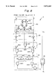
- FIG. 8 is a circuit diagram illustrating a modification of the sense amplifier of FIG. 5.
- reference numeral 1 designates a memory cell array including memory cells (not shown) at intersections between word lines such as WL1 and bit line pairs such as BL 1 and BL 1 .
- an address buffer 2 receives an external address ADD and generates an internal address IADD.
- An X component of the internal address IADD is supplied to a row decoder 3 for selecting one of the word lines, and a Y component of the internal address IADD is supplied to a column decoder 4, so that a column selector 5 selects one pair of the bit line pairs.
- a column decoder 4 for selecting one of the word lines
- a column selector 5 selects one pair of the bit line pairs.
- the internal address IADD is supplied to an address transition detection (ATD) circuit 6 for detecting a transition of the internal address IADD to generate an ATD signal ⁇ ATD .
- ATD address transition detection
- a control circuit 7 receives the ATD signal ⁇ ATD as well as an inverted signal of a write enable signal WE to generate a precharging signal.
- ⁇ PR a sense activation signal ⁇ S and a write activation signal ⁇ W .
- the precharging signal ⁇ PR is supplied to precharging transistors connected to the bit lines, thus precharging the bit lines.
- the sense activation signal ⁇ S is supplied as a sense start signal to a sense amplifier 8, thus activating the sense amplifier 8.
- the write activation signal ⁇ W is supplied to a write amplifier 9, thus activating the write amplifier 9.
- the precharging signal ⁇ PR is generated from the control circuit 7 in synchronization with the ATD signal ⁇ ATD , and thereafter, one memory cell is selected by the row decoder 3 and the column decoder 4 using the internal address IADD.
- the write amplifier circuit 9 is activated, so that potentials at data lines D and D are changed in accordance with input data DI, and the potentials are written into the selected memory cell.
- the precharging signal ⁇ PR is also generated from the control circuit 7 in synchronization with the ATD signal ⁇ ATD , and thereafter, one memory cell is selected by the row decoder 3 and the column decoder 4 using the internal address IADD. As a result, potentials at the data lines D and D are changed in accordance with data in the selected memory cell. In this state, since the sense activation signal ⁇ S is also generated from the control circuit 7, the sense amplifier 8 is activated, so that the potentials at the data lines D and D are amplified, thus obtaining output data DO.
- FIG. 2 which is a detailed circuit diagram of the sense amplifier of FIG. 1, two stages of amplifier circuits 81 and 82, a sense detection circuit 83, a sense end signal generating circuit 84, and an internal sense activation signal generating circuit 85 for activating and deactivating the sense amplifier circuits 81 and 82 are provided.
- the amplifier circuit 81 is of a two end type which amplifies the potentials at the data lines D and D and generates potentials at data lines DOI and DOI.
- the amplifier circuit 81 is formed by a current mirror circuit 811 for receiving the potentials at the data lines D and D, a current mirror circuit 812 for receiving the potentials at the data lines D and D, an N-channel MOS transistor 813 for turning ON and OFF the current mirror circuits 811 and 812, and a P-channel MOS transistor 814 for equalizing the potentials at the data lines D and D.
- the amplifier circuit 82 is of a single end type which amplifies the potentials at the data lines DOI and DOI and generates the output data DO.
- the amplifier circuit 82 is formed by a current mirror circuit 821 for receiving the potentials at the data lines DOI and DOI, an N-channel MOS transistor 822 for turning ON and OFF the current mirror circuit 821, and P-channel MOS transistors 823 and 824 for pulling up the potentials at the data lines DOI and DOI.
- the sense detection circuit 83 is formed by inverters 831 and 832 for receiving the potentials at the data lines DOI and DOI, respectively.
- the inverters 831 and 832 have a common threshold voltage V th which is, in this case, an operating point. If the potential of the DOI is lower than the operating point V th , the inverter 831 generates a sense detection signal N having a high potential. Similarly, if the potential of the DOI is lower than the operating point V th , the inverter 832 generates a sense detection signal N having a high potential.
- the sense end signal generating circuit 84 is formed by delay circuits 841 and 842 connected to the inverters 831 and 832, respectively, a NAND circuit 843 for receiving the sense detection signal N of the inverter 831 and the output of the delay circuit 841, and a NAND circuit 844 for receiving the output potential N of the inverter 832 and the output of the delay circuit 842. Also, a NAND circuit 845 is connected to the outputs of the NAND circuits 843 and 845, for generating a sense end signal SE.
- the sense activation signal generating circuit 85 generates an internal sense activation signal ⁇ SI . That is, the sense activation signal generating circuit 838 includes an RS flip-flop which is set by a rising edge of the sense activation signal ⁇ S and is reset by a rising edge of the sense end signal SE.
- the transistors 813 and 814 of the amplifier circuit 81 and the transistors 822, 823 and 824 of the amplifier circuit 82 are controlled by the internal sense activation signal ⁇ SI .
- the amplifiers 81 and 82 are turned ON and OFF by the internal sense activation signal ⁇ SI , so that the sense amplifier 8 is called a self-cut type sense amplifier.
- the sense activation signal ⁇ S is changed from low to high.
- the internal sense activation signal generating circuit 838 is set, so that the internal sense activation signal ⁇ SI rises at time t2.
- the amplifier circuits 81 and 82 are both activated.
- the amplifier circuit 81 since the current mirror circuits 811 and 812 are cross-coupled, although the potential at one of the data lines such as D remain at a high level, the potential at the other data line such as D is gradually decreased.
- the amplifier circuit 82 the potential at the data lines DOI and DOI are both gradually decreased, but the potential at one of the bit lines such as DOI is again increased.
- the NAND circuits 843, 844 and 845 in combination generate a trigger signal SE. That is, in FIG. 3, at time t3, the potential at the data line DOI becomes lower than the operating point V th , so that the sense detection signal N of the inverter 831 rises. Therefore, at time t4, when a time d corresponding to the delay time of the delay circuit 841 has passed, the sense end signal SE rises to reset the internal sense activation signal generating circuit 85, and accordingly, the internal sense activation signal ⁇ SI falls to deactivate the amplifiers 81 and 82.
- the output data DO is already established at time t5 early enough before time t4, which causes no problem.
- the operation of the sense amplifier 8 of FIG. 2 will be explained next with reference to FIG. 4, where the power supply voltage V CC applied to the sense amplifier 8 is low, for example, 1.5 V.
- the sense activation signal ⁇ S is changed from low to high.
- the internal sense activation signal generating circuit 85 is set, so that the internal sense activation signal ⁇ SI rises at time t2.
- the amplifier circuits 81 and 82 are both activated.
- the potential at one of the data lines such as D remains at a high level, the potential at the other data line such as D is gradually decreased.
- the potentials at the data lines DOI and DOI are both gradually decreased, but the potential at one of the bit lines such as DOI is again increased.
- FIG. 5 which illustrates a first embodiment of the present invention
- a masking circuit 86 is interposed between the sense detection circuit 83 and the sense and signal generating circuit 84 of FIG. 2. That is, when the inverters 831 and 832 simultaneously generate the sense detection signals N and N, the masking circuit 86 disables the sense detection signal N and N, so that the sense end signal generating circuit 84 is not operated.
- the masking circuit 86 is formed by a NOR circuit 861 connected to the data lines DOI and DOI for generating a mask signal MSK.
- the NOR circuit 861 has the same operating point V th as that of the inverters 831 and 832. Therefore, only when the potentials at the data lines DOI and DOI are both lower than the operating point V th , is the mask signal MSK made high.
- the masking circuit 86 is formed by two inverters 862 and 863 connected to the inverters 831 and 832, a NOR circuit 864 connected to the NOR circuit 861 and the inverter 862, and a NOR circuit 865 connected to the NOR circuit 861 and the inverter 863.
- the operation of the sense amplifier 8 of FIG. 2 will be explained next with reference to FIG. 4, where the power supply voltage V CC applied to the sense amplifier 5 is low, for example, 1.5 V.
- the sense activation signal ⁇ S is changed from low to high.
- the internal sense activation signal generating circuit 85 is set, so that the internal sense activation signal ⁇ SI rises at time t2.
- the amplifier circuits 81 and 82 are both activated.
- the potential at one of the data lines such as D remains at a high level, the potential at the other data line such as D is gradually decreased.
- the potentials at the data lines DOI and DOI are both gradually decreased, but the potential at one of the bit lines such as DOI is again increased.
- the mask signal MSK is made low.
- the sense detection signals N and N and the outputs A and A of the inverters 862 and 863 are also changed.
- the sense end signal SE rises to reset the internal sense activation signal generating circuit 85, and accordingly, the internal sense activation signal ⁇ SI falls to deactivate the amplifiers 81 and 82.
- the above-mentioned delay time of the delay circuits 841 and 842 is about 1 to 2 ns.
- the timing of generation of the output data DO can be sufficiently before that of the sense end signal SE, thus making the output data DO normal.
- FIG. 7 which illustrates a second embodiment of the present invention
- the masking circuit 86 of FIG. 5 is modified into a masking circuit 86'.
- the masking circuit 86' is formed by a NAND circuit 861', a NAND circuit 862' and an inverter 863' serving as an AND circuit, a NAND circuit 864' and an inverter 865' serving as an AND circuit, and delay circuits 866' and 867'. NOte that the delay circuits 866' and 867' have a delay time which is approximately the same as the operation time of the NAND circuit 861'. Even in FIG.
- the NAND circuit 861' when the sense detection signals N and N are both high, the NAND circuit 861' generates a mask signal KSK, so that the outputs N1 and N1 of the inverters 863' and 865' are made low regardless of the sense detection signals N and N.
- the sense amplifier 8 of FIG. 7 operates in the same way as the sense amplifier 8 of FIG. 5.
- the present invention can be applied to a sense amplifier including a single differential amplifier as illustrated in FIG. 8, where the amplifier 82 is connected directly to the data lines DO and DO.
- the timing of an output data can be sufficiently before the cut off timing of the sense amplifier.
- normal output data can be obtained.
Landscapes
- Dram (AREA)
- Static Random-Access Memory (AREA)
Applications Claiming Priority (2)
| Application Number | Priority Date | Filing Date | Title |
|---|---|---|---|
| JP8227004A JP2845264B2 (ja) | 1996-08-28 | 1996-08-28 | セルフカットオフ型センスアンプ回路 |
| JP8-227004 | 1996-08-28 |
Publications (1)
| Publication Number | Publication Date |
|---|---|
| US5872465A true US5872465A (en) | 1999-02-16 |
Family
ID=16854009
Family Applications (1)
| Application Number | Title | Priority Date | Filing Date |
|---|---|---|---|
| US08/917,883 Expired - Fee Related US5872465A (en) | 1996-08-28 | 1997-08-27 | Self cut-off type sense amplifier operable over a wide range of power supply voltages |
Country Status (5)
| Country | Link |
|---|---|
| US (1) | US5872465A (fr) |
| EP (1) | EP0827151B1 (fr) |
| JP (1) | JP2845264B2 (fr) |
| KR (1) | KR100263256B1 (fr) |
| DE (1) | DE69717370D1 (fr) |
Cited By (5)
| Publication number | Priority date | Publication date | Assignee | Title |
|---|---|---|---|---|
| US6114881A (en) * | 1997-06-24 | 2000-09-05 | Hyundai Electronics Industries Co., Ltd. | Current mirror type sense amplifier |
| US6304107B1 (en) * | 2000-02-25 | 2001-10-16 | Lsi Logic Corporation | Comparator metastability performance from an enhanced comparator detection circuit |
| US20030218481A1 (en) * | 2002-05-02 | 2003-11-27 | Bernhard Wicht | Differential current evaluation circuit and sense amplifier circuit for evaluating a memory state of an SRAM semiconductor memory cell |
| US20130293300A1 (en) * | 2012-05-04 | 2013-11-07 | SK Hynix Inc. | Input/output sense amplifier and semiconductor apparatus including the same |
| CN116430102A (zh) * | 2023-06-14 | 2023-07-14 | 苏州贝克微电子股份有限公司 | 一种宽输入电压范围的电压检测电路 |
Families Citing this family (6)
| Publication number | Priority date | Publication date | Assignee | Title |
|---|---|---|---|---|
| US6025741A (en) * | 1996-12-23 | 2000-02-15 | International Business Machines Corporation | Conditional restore for execution unit |
| US6282137B1 (en) * | 1999-09-14 | 2001-08-28 | Agere Systems Guardian Corp. | SRAM method and apparatus |
| JP2001101872A (ja) | 1999-09-30 | 2001-04-13 | Mitsubishi Electric Corp | 増幅回路 |
| KR100483028B1 (ko) * | 2003-03-19 | 2005-04-15 | 주식회사 하이닉스반도체 | 강유전체 메모리 셀 및 이를 이용한 메모리 장치 |
| EP2124337B1 (fr) * | 2008-05-23 | 2016-04-27 | Zoran Corporation | Circuit comparateur verrouillé |
| US8319526B2 (en) | 2009-11-17 | 2012-11-27 | Csr Technology Inc. | Latched comparator circuit |
Citations (7)
| Publication number | Priority date | Publication date | Assignee | Title |
|---|---|---|---|---|
| EP0435581A2 (fr) * | 1989-12-27 | 1991-07-03 | Motorola, Inc. | Etage d'amplification de sortie avec propriÀ©té d'économiser de la puissance |
| US5155397A (en) * | 1989-12-22 | 1992-10-13 | Cselt - Centro Studi E Laboratori Telecomunicazioni S.P.A. | C-mos differential sense amplifier |
| US5329494A (en) * | 1991-03-07 | 1994-07-12 | Kabushiki Kaisha Toshiba | Memory cell array divided type semiconductor memory device |
| US5434824A (en) * | 1993-07-21 | 1995-07-18 | Fujitsu Limited | Semiconductor memory device with reduced power consumption and reliable read mode operation |
| US5479374A (en) * | 1992-05-27 | 1995-12-26 | Kabushiki Kaisha Toshiba | Semiconductor memory device employing sense amplifier control circuit and word line control circuit |
| US5729499A (en) * | 1995-04-06 | 1998-03-17 | Ricoh Company, Ltd. | Sense amplifier and reading circuit with sense amplifier |
| US5742549A (en) * | 1995-11-13 | 1998-04-21 | Micron Technology, Inc. | Sense amplifier circuit for detecting degradation of digit lines and method thereof |
-
1996
- 1996-08-28 JP JP8227004A patent/JP2845264B2/ja not_active Expired - Fee Related
-
1997
- 1997-08-27 US US08/917,883 patent/US5872465A/en not_active Expired - Fee Related
- 1997-08-28 EP EP97114945A patent/EP0827151B1/fr not_active Expired - Lifetime
- 1997-08-28 DE DE69717370T patent/DE69717370D1/de not_active Expired - Lifetime
- 1997-08-28 KR KR1019970045784A patent/KR100263256B1/ko not_active Expired - Fee Related
Patent Citations (7)
| Publication number | Priority date | Publication date | Assignee | Title |
|---|---|---|---|---|
| US5155397A (en) * | 1989-12-22 | 1992-10-13 | Cselt - Centro Studi E Laboratori Telecomunicazioni S.P.A. | C-mos differential sense amplifier |
| EP0435581A2 (fr) * | 1989-12-27 | 1991-07-03 | Motorola, Inc. | Etage d'amplification de sortie avec propriÀ©té d'économiser de la puissance |
| US5329494A (en) * | 1991-03-07 | 1994-07-12 | Kabushiki Kaisha Toshiba | Memory cell array divided type semiconductor memory device |
| US5479374A (en) * | 1992-05-27 | 1995-12-26 | Kabushiki Kaisha Toshiba | Semiconductor memory device employing sense amplifier control circuit and word line control circuit |
| US5434824A (en) * | 1993-07-21 | 1995-07-18 | Fujitsu Limited | Semiconductor memory device with reduced power consumption and reliable read mode operation |
| US5729499A (en) * | 1995-04-06 | 1998-03-17 | Ricoh Company, Ltd. | Sense amplifier and reading circuit with sense amplifier |
| US5742549A (en) * | 1995-11-13 | 1998-04-21 | Micron Technology, Inc. | Sense amplifier circuit for detecting degradation of digit lines and method thereof |
Cited By (9)
| Publication number | Priority date | Publication date | Assignee | Title |
|---|---|---|---|---|
| US6114881A (en) * | 1997-06-24 | 2000-09-05 | Hyundai Electronics Industries Co., Ltd. | Current mirror type sense amplifier |
| US6304107B1 (en) * | 2000-02-25 | 2001-10-16 | Lsi Logic Corporation | Comparator metastability performance from an enhanced comparator detection circuit |
| US20030218481A1 (en) * | 2002-05-02 | 2003-11-27 | Bernhard Wicht | Differential current evaluation circuit and sense amplifier circuit for evaluating a memory state of an SRAM semiconductor memory cell |
| DE10219649C1 (de) * | 2002-05-02 | 2003-11-27 | Infineon Technologies Ag | Differentielle Strombewerterschaltung und Leseverstärkerschaltung zum Bewerten eines Speicherzustands einer SRAM-Halbleiterspeicherzelle |
| US7099218B2 (en) | 2002-05-02 | 2006-08-29 | Infineon Technologies Ag | Differential current evaluation circuit and sense amplifier circuit for evaluating a memory state of an SRAM semiconductor memory cell |
| US20130293300A1 (en) * | 2012-05-04 | 2013-11-07 | SK Hynix Inc. | Input/output sense amplifier and semiconductor apparatus including the same |
| US8797068B2 (en) * | 2012-05-04 | 2014-08-05 | SK Hynix Inc. | Input/output sense amplifier and semiconductor apparatus including the same |
| CN116430102A (zh) * | 2023-06-14 | 2023-07-14 | 苏州贝克微电子股份有限公司 | 一种宽输入电压范围的电压检测电路 |
| CN116430102B (zh) * | 2023-06-14 | 2023-08-29 | 苏州贝克微电子股份有限公司 | 一种宽输入电压范围的电压检测电路 |
Also Published As
| Publication number | Publication date |
|---|---|
| JPH1069785A (ja) | 1998-03-10 |
| KR19980019216A (ko) | 1998-06-05 |
| DE69717370D1 (de) | 2003-01-09 |
| KR100263256B1 (ko) | 2000-08-01 |
| EP0827151B1 (fr) | 2002-11-27 |
| JP2845264B2 (ja) | 1999-01-13 |
| EP0827151A1 (fr) | 1998-03-04 |
Similar Documents
| Publication | Publication Date | Title |
|---|---|---|
| US20060028888A1 (en) | Semiconductor memory device having local sense amplifier with on/off control | |
| US5455803A (en) | Semiconductor device which operates at a frequency controlled by an external clock signal | |
| US5966319A (en) | Static memory device allowing correct data reading | |
| JP2003036678A (ja) | セルフタイミング回路を有するスタティックメモリ | |
| JPH05325540A (ja) | 半導体記憶回路 | |
| US5872465A (en) | Self cut-off type sense amplifier operable over a wide range of power supply voltages | |
| JPH05282868A (ja) | 半導体記憶装置 | |
| KR100297717B1 (ko) | 반도체메모리의입출력선프리차아지회로및이를사용하는반도체메모리 | |
| KR100297708B1 (ko) | 클락동기프리차아지데이터입출력선을가지는반도체메모리장치및이를이용한데이터입출력선프리차아지방법 | |
| US5825715A (en) | Method and apparatus for preventing write operations in a memory device | |
| US6411559B1 (en) | Semiconductor memory device including a sense amplifier | |
| JP3308572B2 (ja) | 半導体装置 | |
| KR20000008774A (ko) | 동기식 디램의 자동 프리차지 장치 | |
| KR100402388B1 (ko) | 칩선택 출력 시간이 단축된 반도체 메모리 장치 | |
| JPH06176568A (ja) | 半導体記憶装置 | |
| US5648932A (en) | Output control circuit for semiconductor memory | |
| US6134174A (en) | Semiconductor memory for logic-hybrid memory | |
| US5973987A (en) | Semiconductor memory device delaying ATD pulse signal to generate word line activation signal | |
| KR100431477B1 (ko) | 반도체메모리장치 | |
| US6169702B1 (en) | Memory device having a chip select speedup feature and associated methods | |
| US5355349A (en) | Semiconductor integrated circuit device | |
| US5377157A (en) | Multiport memory | |
| KR100301820B1 (ko) | 센스 앰프 | |
| JP3192709B2 (ja) | 半導体記憶装置 | |
| KR100481827B1 (ko) | 데이터입/출력버퍼회로를제어하기위한회로들을갖는반도체메모리장치 |
Legal Events
| Date | Code | Title | Description |
|---|---|---|---|
| AS | Assignment |
Owner name: NEC CORPORATION, JAPAN Free format text: ASSIGNMENT OF ASSIGNORS INTEREST;ASSIGNOR:SAITOH, TOSHIO;REEL/FRAME:008786/0841 Effective date: 19970822 |
|
| FEPP | Fee payment procedure |
Free format text: PAYOR NUMBER ASSIGNED (ORIGINAL EVENT CODE: ASPN); ENTITY STATUS OF PATENT OWNER: LARGE ENTITY |
|
| FPAY | Fee payment |
Year of fee payment: 4 |
|
| REMI | Maintenance fee reminder mailed | ||
| LAPS | Lapse for failure to pay maintenance fees | ||
| STCH | Information on status: patent discontinuation |
Free format text: PATENT EXPIRED DUE TO NONPAYMENT OF MAINTENANCE FEES UNDER 37 CFR 1.362 |
|
| FP | Lapsed due to failure to pay maintenance fee |
Effective date: 20070216 |