EP0827304A2 - Synchronisateur utilisant un motif connu de transmission - Google Patents
Synchronisateur utilisant un motif connu de transmission Download PDFInfo
- Publication number
- EP0827304A2 EP0827304A2 EP97305702A EP97305702A EP0827304A2 EP 0827304 A2 EP0827304 A2 EP 0827304A2 EP 97305702 A EP97305702 A EP 97305702A EP 97305702 A EP97305702 A EP 97305702A EP 0827304 A2 EP0827304 A2 EP 0827304A2
- Authority
- EP
- European Patent Office
- Prior art keywords
- timing
- circuit
- difference
- receiver
- time
- Prior art date
- Legal status (The legal status is an assumption and is not a legal conclusion. Google has not performed a legal analysis and makes no representation as to the accuracy of the status listed.)
- Withdrawn
Links
Images


Classifications
-
- H—ELECTRICITY
- H04—ELECTRIC COMMUNICATION TECHNIQUE
- H04L—TRANSMISSION OF DIGITAL INFORMATION, e.g. TELEGRAPHIC COMMUNICATION
- H04L25/00—Baseband systems
- H04L25/38—Synchronous or start-stop systems, e.g. for Baudot code
- H04L25/40—Transmitting circuits; Receiving circuits
- H04L25/49—Transmitting circuits; Receiving circuits using code conversion at the transmitter; using predistortion; using insertion of idle bits for obtaining a desired frequency spectrum; using three or more amplitude levels ; Baseband coding techniques specific to data transmission systems
- H04L25/493—Transmitting circuits; Receiving circuits using code conversion at the transmitter; using predistortion; using insertion of idle bits for obtaining a desired frequency spectrum; using three or more amplitude levels ; Baseband coding techniques specific to data transmission systems by transition coding, i.e. the time-position or direction of a transition being encoded before transmission
-
- H—ELECTRICITY
- H04—ELECTRIC COMMUNICATION TECHNIQUE
- H04L—TRANSMISSION OF DIGITAL INFORMATION, e.g. TELEGRAPHIC COMMUNICATION
- H04L7/00—Arrangements for synchronising receiver with transmitter
- H04L7/04—Speed or phase control by synchronisation signals
- H04L7/041—Speed or phase control by synchronisation signals using special codes as synchronising signal
- H04L7/042—Detectors therefor, e.g. correlators, state machines
Definitions
- the present invention relates to a synchronizer for a communication system, or more in particular to a synchronizer in which a timing deviation can be estimated based on the average value of the difference in frame timing even in the case where a unique word (UW) pattern fails to be received, thereby making it possible to hold a frame timing even after a protracted line disconnection.
- UW unique word
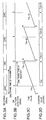
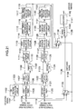
- a conventional synchronizer of this type as shown in Fig. 1A, comprises a UW pattern detection circuit 2, a reference timer 5, a latch circuit 6, a histogram calculation circuit 8, a timing correction value calculation circuit 10, and a decoder 13.
- the UW pattern detection circuit 2 detects a unique word pattern (hereinafter referred to as "the UW pattern") contained in a known symbol pattern (normally called “the synchronous word” or "the unique word”) of a receiving signal 1 shown in Fig. 1B.
- the reference timer 5 calculates the receiving time based on a reference clock 4.
- the latch circuit 6 fetches the time when the UW pattern is detected (the UW pattern detection time) by latching an output signal of the reference timer 5 by an output signal 3 of the UW pattern detection circuit 2.
- the histogram calculation circuit 8 calculates the histogram of the UW pattern detection time from an output signal 7 of the latch circuit 6 and further calculates the difference between the frame timing of a transmitter and the frame timing of a receiver based on the calculated histogram and an output signal 12 of the timing correction value calculation circuit 10.
- the timing correction value calculation circuit 10 produces on the basis of an output signal 9 of the histogram calculation circuit 8 a control signal 11 to be output to the reference timer 5 for correcting the frame timing of the receiver in the forward direction when deviated backward of the frame timing of the transmitter and backward when deviated forward of the frame timing of the transmitter. Specifically, in correcting the frame timing of the receiver in forward direction, the initial value of the reference timer 5 is set to +1 by the control signal 11, while in correcting the frame timing of the receiver backward, the initial value of the reference timer 5 is set to -1 by the control signal 11. In this way, the frame length is increased or decreased by one frame, as the case may be, to set the frame timing of the receiver to conform with that of the transmitter.
- the frame timing of the receiver is corrected by detecting the UW pattern constantly and thus by detecting the difference between the frame timing of the receiver and that of the transmitter.
- the UW pattern cannot be detected over a long time due to a line disconnection or the like, the frame timing of the receiver and that of the transmitter are deviated considerably from each other.
- the object of the present invention is to provide a synchronizer in which the frame timing of the receiver and that of the transmitter are prevented from deviating from each other considerably even in the case where a known symbol pattern fails to be detected over a long time due to a line connection or the like.
- a synchronizer in which an average value of a difference between a frame timing of a receiver and a frame timing of a transmitter is calculated, the average value of the difference in frame timing is integrated at intervals of a predetermined frame time, and the timing is corrected based on the integrated value of timing deviations. Consequently, even in the case where the UW pattern fails to be detected, the timing deviation can be estimated based on the average value of the difference in frame timing. Even in the case where the line is disconnected over a long time, therefore, the appropriate frame timing can be held.
- a synchronizer which comprises a detection circuit for detecting a difference between a reference timing of a transmitter and a reference timing of a receiver based on a time of receiving a known transmission pattern transmitted from the transmitter, an average value calculation circuit for calculating an average value of the detected difference, an integration circuit for integrating the average value each time of interrupting the receiver and determining an integrated value, and a correction value calculation circuit for correcting the reference timing of the receiver in forward direction in the case where the integrated value is larger than a first threshold value and correcting the reference timing of the receiver backward in the case where the integrated value is smaller than a second threshold value.
- Fig. 1A is a block diagram showing a conventional synchronizer.
- Fig. 1B is a diagram for explaining a frame format.
- Fig. 2 is a block diagram showing a synchronizer according to a first embodiment of the present invention.
- Figs. 3A to 3D are diagrams for explaining the operation of the synchronizer shown in Fig. 2.
- Figs. 4A to 4D are diagrams for explaining the operation of the synchronizer shown in Fig. 2.
- Fig. 5 is a block diagram showing a synchronizer according to a second embodiment of the present invention.
- Figs. 6A to 6D are diagrams for explaining the operation of the synchronizer shown in Fig. 5.
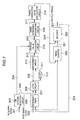
- Fig. 7 is a block diagram showing a synchronizer according to a third embodiment of the present invention.
- Figs. 8A to 8E are diagrams for explaining the operation of the synchronizer shown in Fig. 7.
- Fig. 9 is a block diagram showing a synchronizer according to a fourth embodiment of the present invention.
- Figs. 10A to 10E are diagrams for explaining the operation of the synchronizer shown in Fig. 9.
- Fig. 11 is a block diagram showing a synchronizer according to a fifth embodiment of the present invention.
- Figs. 12A and 12B are diagrams for explaining the operation of the synchronizer shown in Fig. 11.
- Fig. 13 is a block diagram showing a synchronizer according to sixth and seventh embodiments of the present invention.
- Fig. 14 is a diagram for explaining the operation of the synchronizer shown in Fig. 13.
- Fig. 15 is a block diagram showing a synchronizer according to an eighth embodiment of the present invention.
- Fig. 16 is a diagram for explaining the operation of the synchronizer shown in Fig. 15.
- Fig. 17 is a block diagram showing a synchronizer according to a ninth embodiment of the present invention.
- Fig. 18 is a diagram for explaining the operation of the synchronizer shown in Fig. 17.
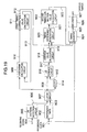
- Fig. 19 is a block diagram showing a synchronizer according to a tenth embodiment of the present invention.
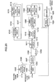
- Fig. 20 is a block diagram showing a synchronizer according to an eleventh embodiment of the present invention.
- Fig. 21 is a block diagram showing a synchronizer according to a twelfth embodiment of the present invention.
- a synchronizer comprises, as shown in Fig. 2, a UW pattern detection circuit 102, a reference timer 105, a latch circuit 107, a D flip-flop (D-FF) circuit 109, a difference circuit 111, an average value calculation circuit 113, a timing difference integration circuit 115, a timing correction value calculation circuit 117, a timing counter 119 and a decoder 121.
- D-FF D flip-flop
- the UW pattern detection circuit 102 detects a UW pattern (Fig. 1B) contained in a receiving signal 101. Upon detection of the UW pattern, a UW pattern detection signal 103 is output and a UW pattern detection information signal 123, which indicates whether or not the UW pattern is detected, is generated.
- the reference timer 105 calculates a receiving time based on a reference clock 104.
- the latch circuit 107 latches an output signal 106 of the reference timer 105 by the UW pattern detection signal 103 from the UW pattern detection circuit 102 thereby to fetch a time (UW pattern detection time) when the UW pattern is detected.
- the D flip-flop circuit 109 holds the UW pattern detection time fetched into the latch circuit 107.
- the difference circuit 111 determines a difference (frame timing difference) between a frame timing of the transmitter and a frame timing of the receiver based on a difference between an output signal 108 of the latch circuit 107 and an output signal 110 of the D flip-flop circuit 109.
- the average value calculation circuit 113 updates an average value of the frame timing difference calculated based on an output signal 112 of the difference circuit 111 only when the detection of the UW pattern is indicated by the UW pattern detection information signal 123 from the UW pattern detection circuit 102.
- the timing difference integration circuit 115 integrates the average value of the frame timing difference based on an output signal 114 of the average value calculation circuit 113.
- the timing correction value calculation circuit 117 produces a control signal 118 for the timing counter 119 on the basis of an output signal 116 of the timing difference integration circuit 115 in order to correct the frame timing of the receiver in forward direction in the case where it is deviated backward of the frame timing of the transmitter on the one hand and to correct the frame timing of the receiver backward in the case where it is deviated forward of the frame timing of the transmitter on the other hand.
- an initial value of the timing counter 119 is set to +1 by the control signal 118, while in the case where the frame timing of the receiver is corrected backward, the initial value of the timing counter 119 is set to -1 by the control signal 118.
- the frame length is increased or decreased, as the case may be, by one frame thereby to set the frame timing of the receiver to conform with the frame timing of the transmitter.
- the timing counter 119 counts the reference clock 104 by a period of one frame with the initial value set by the control signal 118 from the timing correction value calculation circuit 117.
- the decoder 121 generates various timings 122 based on an output signal 120 of the timing counter 119.
- the receiving signal 101 inserts therein the UW pattern for each frame as shown in Fig. 3A.
- the receiving signal 101 is transmitted based on the frame timing of the transmitter.
- the one-frame time of the transmitter can be detected, therefore, by detecting the intervals at which the UW patterns contained in the receiving signal 101 are received.
- UW pattern detection time T(k+1) is detected by the value on a timer built therein. The difference is determined between UW pattern detection time T(k+1) detected in the current frame and UW pattern detection time T(k) detected in the previous frame thereby to determine the one-frame time of the receiver (Fig. 3B).
- the one-frame time of the receiver can be determined from the modulo calculation shown below. ⁇ T(k+1) + N - T(k) ⁇ modulo N
- the difference between the value determined by equation (1-1) above and the standard frame time length constitutes the difference between the frame timing of the receiver and that of the transmitter.
- the timing correction value calculation circuit 117 performs the following processes:
- Figs. 4A to 4D show an example of correcting the frame timing of the receiver by one in forward direction. This shows the manner in which the timing generated is corrected in forward direction by one by increasing the initial value of the timing counter 119 by one frame.
- the average value calculation circuit 113 performs the following processes based on the UW pattern detection information signal 123 from the UW pattern detection circuit 102:
- the synchronizer according to this embodiment can correct the timing using the average value of the frame timing difference which is not updated.
- a synchronizer according to a second embodiment of the present invention is different from the synchronizer according to the first embodiment in that a timing counter 205 operates as the reference timer 105 shown in Fig. 2 at the same time.
- the UW pattern receiving time is detected using the reference timer 105. Consequently, the clock rate of the timing counter 119 is normally the same as the symbol rate or the bit rate. It is therefore possible to detect the UW pattern receiving time with a higher accuracy by increasing the clock rate of the reference timer 105 as compared with that of the timing counter 119.
- Such a synchronizer requires two counters for the reference counter 105 and the timing counter 119, and therefore increases in circuit size and power consumption.
- the synchronizer is adapted to detect the receiving time of the UW pattern as well using the timing counter 205.
- a latch circuit 207 is supplied with an output signal 206 of the timing counter 205.
- a D flip-flop (D-FF) circuit 221 for holding a control signal 218 output from a timing correction value calculation circuit 217 is inserted between the timing correction value calculation circuit 217 and an average value calculation circuit 213.
- a UW pattern detection circuit 202 detects a UW pattern contained in a receiving signal 201. Upon detection of the UW pattern, a UW pattern detection signal 203 is output and a UW pattern detection information signal 223, which indicates whether or not the UW pattern is detected, is generated.
- the latch circuit 207 latches the output signal 206 of the timing counter 205 by the UW pattern detection signal 203 from the UW pattern detection circuit 202, thereby fetching a time when the UW pattern is detected (UW pattern detection time).
- a D flip-flop circuit 209 holds the UW pattern detection time fetched into the latch circuit 207.
- the difference circuit 211 determines a difference between the frame timing of the transmitter and that of the receiver (frame timing difference) based on the difference between an output signal 208 of the latch circuit 207 and an output signal 210 of the D flip-flop circuit 209.
- the UW pattern detection time is detected using the timing counter 205 corrected in timing.
- the frame timing difference determined by the difference circuit 211 is increased or decreased by the amount of the timing correction.
- the D flip-flop circuit 221 holds the control signal 218 from the timing correction value calculation circuit 217, and the frame timing difference determined by the difference circuit 211 is corrected in the average value calculation circuit 213 in accordance with the timing correction value indicated by an output signal 222 of the D flip-flop circuit 221.
- the average value calculation circuit 213 updates the average value of the corrected frame timing difference only when the UW pattern detection information signal 223 from the UW pattern detection circuit 202 indicates that the UW pattern is detected.
- a timing difference integration circuit 215 integrates the average value of the frame timing difference based on an output signal 214 of the average value calculation circuit 213.
- the timing correction value calculation circuit 217 On the basis of an output signal 216 of the timing difference integration circuit 215, the timing correction value calculation circuit 217 generates the control signal 218 for the timing counter 205 in order to correct the frame timing of the receiver in forward direction, if deviated backward of that of the transmitter, and to correct the frame timing of the receiver backward, if deviated forward of the frame timing of the transmitter. Specifically, in the case of correcting the frame timing of the receiver in forward direction, the initial value of the timing counter 205 is set to +1 by the control signal 218, while in the case of correcting the frame timing of the receiver backward, the initial value of the timing counter 205 is set to -1 by the control signal 218.
- the frame timing of the receiver is set to conform with that of the transmitter by increasing or decreasing, as the case may be, the frame length by one frame.
- the timing counter 205 counts a reference clock 204 by frame period with the initial value set by the control signal 218 from the timing correction value calculation circuit 217.
- a decoder 219 generates various timings 220 based on the output signal 206 of the timing counter 205.
- the receiving signal 201 inserts therein the UW pattern in each frame thereof.
- the timing is corrected during the period from the time when the second UW pattern from the left is received to the time when the third UW pattern is received.
- the initial value of the timing counter 205 thus is set to +1 as shown in Fig. 6C.
- the UW pattern detection time points fetched into the latch circuit 207 the respective frames are assumed to be t(k), t(k+1), t(k+2), t(k+3), respectively, as shown in Fig. 6D.
- the UW pattern detection time points t(k), t(k+1), t(k+2), t(k+3) for the respective frames have equal intervals.
- the UW pattern detection time points t(k+2), t(k+3) for the third and subsequent frames from the left in the diagram are deviated to assume a value larger by one than the UW pattern detection time points t(k), t(k+1) for the first and second frames from left, respectively. Consequently, the frame timing difference calculated by the difference circuit 211 is given by the equation shown below.
- a synchronizer according to a third embodiment of the present invention is different from the synchronizer according to the first embodiment shown in Fig. 2 in that a reference timer control signal 324 is output to a reference timer 306 from a decoder 322 and that a control signal 319 output from a timing correction value calculation circuit 318 is applied also to the decoder 322.
- the reference timer 105 is used for counting a period longer than the one-frame time, while the synchronizer according to the second embodiment uses the timing counter 205 for counting the same period as the one-frame time.
- An increased number of symbols or bits per frame is accompanied by an increased number of bits of the counter, an increased number of bits of the latch circuit, an increased number of bits of the D flip-flop circuit for holding the UW pattern detection time for the immediately preceding frame and an increased number of bits of the difference circuit, thereby leading to an increased power consumption and an increased circuit size.
- the reference timer control signal 324 is applied to the reference timer 306 from the decoder 322 in order to reduce the number of bits of the counter making up the reference timer 306.
- the basic operation of the synchronizer according to this embodiment is similar to that of the synchronizer according to the first embodiment.
- a method of producing the reference timer control signal 324 will be explained below.
- the decoder 322 produces the reference timer control signal 324 based on an output signal 321 of a timing counter 320.
- This reference timer control signal 324 activates the reference timer 306 a little before an assumed UW pattern receiving time, and deactivates the reference timer 306 a little after the assumed UW pattern receiving time.
- the decoder 322 corrects the time to activate the reference timer 306 by the amount of correction value of the timing counter 320 based on the control signal 319 of the timing correction value calculation circuit 318.
- the reference timer 306 is operated based on the reference timer control signal 324 produced in the manner described above thereby to produce the following effects:
- a synchronizer according to a fourth embodiment of the present invention is different from the synchronizer according to the third embodiment, as shown in Fig. 9, in that a switch 406 is provided on the input side of a reference timer 408 for switching the application and non-application of a reference clock 405 to the reference timer 408 in accordance with a reference timer control signal 426 from a decoder 424 and a UW pattern detection signal 403 from a UW pattern detection circuit 402.
- the synchronizer according to the third embodiment described above activates the reference timer 306 a little before the assumed UW pattern receiving time and deactivates the reference timer 306 a little after the assumed UW pattern receiving time.
- the power consumption of the counter constituting the reference timer 306 increases in the following cases:
- the synchronizer comprises the switch 406 and controls the operation of the reference timer 408 in the following manner:
- the basic operation of the synchronizer according to this embodiment is similar to that of the synchronizer according to the third embodiment described above.
- a method of controlling the switching operation of the switch 406 will be described. Assume that the reference timer 408 is activated at the leading edge of the reference timer control signal 426 from the decoder 424, as shown in Figs. 10A, 10D. (1) In the case where a UW pattern is detected in the UW pattern detection circuit 402:
- the reference timer 408 is activated at the leading edge of the reference timer control signal 426 from the decoder 424 (Figs. 10A to 10C).
- UW pattern detection time T(k) is fetched into a latch circuit 410 by the UW pattern detection signal 403 (Figs. 10D, 10E).
- the switch 406 is opened by the UW pattern detection signal 403, so that the reference clock 405 stops being applied to the reference timer 408 and a count value of the counter making up the reference timer 408 is reset (Fig. 10D).
- the reference timer 408 is deactivated at the falling edge of the reference timer control signal 426 (Fig. 10D).
- the reference timer 408 is activated at the leading edge of the reference timer control signal 426 from the decoder 424 (Figs. 10A to 10C).
- the UW pattern detection signal 403 is not output from the UW pattern detection circuit 402 (Fig. 10C), and therefore the counter making up the reference timer 408 continues to count.
- the reference timer 408 is deactivated at the falling edge of the reference timer control signal 426 (Fig. 10D).
- the UW pattern detection time fetched into the latch circuit 410 remains at the previous UW pattern detection time T(k) (Fig. 10E). An updating of an average value in an average value detection circuit 416 is thus prohibited by a UW pattern detection information signal 404.
- the synchronizer according to this embodiment can realize a low power consumption by shortening the operation time of the reference timer 408.
- a synchronizer according to a fifth embodiment of the present invention is different from the synchronizer according to the second embodiment described above in that a symbol synchronizing circuit 502 supplied with a receiving signal 501 is provided on the input side of a difference circuit 514, that a D flip-flop (D-FF) circuit 526 for holding an output signal 503 (a symbol synchronization signal for the immediately preceding period) of the symbol synchronizing circuit 502 is provided on the input side of the difference circuit 514, and that the differentiation circuit 514 detects the difference between the frame timing of the transmitter and that of the receiver using the output signal 503 of the symbol synchronizing circuit 502 and an output signal 527 of the D flip-flop circuit 526.
- D-FF D flip-flop
- the synchronizer according to this embodiment is adapted to detect the UW pattern receiving time with an accuracy N times higher than the symbol time accuracy.
- the receiving signal 501 is assumed to include a symbol string changing in polarity at every symbol period in order to easily achieve the symbol synchronism.
- the symbol synchronizing circuit 502 decides that a point m(k) assuming the maximum sum y(k) represents the symbol ID point for the kth frame.
- the symbol ID point m(k) thus decided is stored in the D flip-flop circuit 526.
- the difference circuit 514 determines the difference between the frame timing of the transmitter and that of the receiver according to the following equation: ⁇ t(k+1) + m(k+1)/N ⁇ - ⁇ t(k) + m(k)/N ⁇ where t(k+1) and t(k) are the UW pattern detection time for the (k+1)th frame and the kth frame, respectively, which are applied to the difference circuit 514 from a latch circuit 510 and a D flip-flop circuit 512. Consequently, the difference circuit 514 can determine the difference between the frame timing of the transmitter and that of the receiver using the UW pattern detection time N times as accurate as the symbol time.
- the envelope of the receiving signal 501 can be added as an alternative.
- a synchronizer according to a sixth embodiment of the present invention is adapted to detect the difference between the frame timing of the transmitter and that of the receiver by receiving an arbitrary slot within a given frame.
- each frame is configured of access channels A1, A2, control channels C1 to C8 and user channels U1 to U16, for example, as shown in Fig. 14.
- the access channels A1, A2 are used for notification from a base station and the position registration from a mobile unit.
- the control channels C1 to C8 are used for allotment of the user channels U1 to U16, etc.
- the user channels U1 to U16 are used for transmitting and receiving data.
- a synchronism holding circuit receives the UW pattern transmitted from the base station using the forward-link access channel A1 thereby to achieve the frame synchronism. Also, a timing generating circuit generates a timing by frame using the information on the frame structure held therein. On the basis of this timing by frame, the control channel as designated using the forward-link access channel A1 by the base station is transmitted or received, or the data are transmitted or received using the user channel allotted from the base station by the particular control channel.
- the standard time differences (counts) Tu1c1, Tu2u1, Tu2c1 are stored in a memory 626.
- the count difference on the frame counter between the time when the UW pattern contained in the forward-link control channel C1 is detected and the time when the UW pattern contained in the forward-link user channel U1 is detected is expressed as tu1(k) - tc1(k)
- the count difference on the frame counter between the time when the UW pattern contained in the forward-link user channel U1 is detected and the time when the UW pattern contained in the forward-link user channel U2 is detected is expressed as follows. tu2(k) - tu1(k)
- the count difference on the frame counter between the time when the UW pattern contained in the forward-link control channel C1 is detected and the time when the UW pattern contained in the forward-link user channel U2 is detected is expressed as tc1(k) - tu2(k)
- the count difference on the frame counter between the time when the UW pattern contained in the forward-link control channel C1 is detected and the time when the UW pattern contained in the forward-link user channel U1 is detected is expressed as follows. tu1(k+1) - tc1(k+1)
- the count difference on the frame counter between the time when the UW pattern contained in the forward-link user channel U1 is detected and the time when the UW pattern contained in the forward-link user channel U2 is detected is expressed as tu2(k+1) - tu1(k+1)
- the count difference on the frame counter between the time when the UW pattern contained in the forward-link control channel C1 is detected and the time when the UW pattern contained in the forward-link user channel U2 is detected is expressed as follows. tc1(k+1) - tu2(k+1)
- the timing deviation between the transmitter and the receiver between corresponding channels in a given frame can be calculated, therefore, by subtracting the corresponding standard time difference (count) from the results obtained by equations (4-1) to (4-6). It is possible, for example, to calculate the timing deviation between the transmitter and the receiver up to the forward-link user channel U1 from the forward-link control channel C1 by subtracting the standard time difference (count) Tu1c1 from the result tu1(k) - tc1(k) obtained according to equation (4-1) above.
- the synchronizer according to this embodiment, as shown in Fig. 13, comprises the memory 626 for storing the standard time difference (count) corresponding to a channel type 624 and a slot number 625, so that the standard time difference (count) is read out of the memory 626 according to the channel type 624 and the slot number 625.
- the difference circuit 611 calculates the timing deviation between the transmitter and the receiver using an output signal 608 (say, time tu1(k)) of a latch circuit 607, an output signal 610 (say, time tc1(k)) of a D flip-flop circuit 609 and the standard time difference (say, the standard time Tu1c1) read out of the memory 626.
- a synchronizer according to the present embodiment using the standard time difference (count) based on the channel type and the slot number is applicable also to the synchronizer according to the second to the fifth embodiments described above.
- a synchronizer according to a seventh embodiment of the present invention is different from the synchronizer according to the sixth embodiment described above in that an output signal 627 of the memory 626 is applied also to an average value calculation circuit 613, as shown by a dashed line in Fig. 13.
- the synchronizer according to the sixth embodiment concerns a method of detecting the difference in the receiving time of a known pattern (UW pattern) by channel type and slot number
- the synchronizer according to the seventh embodiment is adapted to calculate the average value of the timing difference between the transmitter and the receiver without regard to the channel type or slot number.
- Each timing difference per symbol time is expressed as follows. (tu1(k) - tc1(k) - Tu1c1)/Tu1c1 (tu2(k) - tu1(k) - Tu2u1)/Tu2u1 (tc1(k) - tu2(k) - Tu2c1)/Tu2c1 (tu1(k+1) - tc1(k+1) - Tu1c1)/Tu1c1 (tu2(k+1) - tu1(k+1) - Tu2u1)/Tu2u1 (tc1(k+1) - tu2(k+1) - Tu2c1)/Tu2c1 (tc1(k+1) - tu2(k+1) - Tu2c1)/Tu2c1
- the timing difference between the transmitter and the receiver per frame can be calculated by multiplying the results obtained from equations (5-1) and (5-5) by the number of symbols per frame (TFL).
- the memory 626 is supplied with the the channel type 624 and the slot number 625 for the UW pattern contained in the forward-link control channel C1, together with the channel type 624 and the slot number 625 for the UW pattern contained in the forward-link user channel U1. Consequently, the standard time difference Tulcl between the forward-link user channel U1 and the forward-link control channel C1 is read out of the memory 626 and applied to the difference circuit 611 and the average value calculation circuit 613.
- the difference circuit 611 calculates the numerator of equation (5-1) using the UW pattern detection time tul fetched into the latch circuit 607, the UW pattern detection time tcl held in the D flip-flop circuit 609 and the standard time difference Tulcl from the memory 626.
- the average value calculation circuit 613 calculates the equation (5-1) described above using an output signal 612 of the difference circuit 611 and the standard time difference Tulcl from the memory 626. As a consequence, the timing difference between the transmitter and the receiver per symbol is calculated.
- An output signal 614 of the average value calculation circuit 613 is integrated at a timing difference integration circuit 615. After that, a timing correction value calculation circuit 617 corrects the timing using an output signal 616 of the timing difference integration circuit 615.
- the average value calculation circuit 613 calculates the timing difference between the transmitter and the receiver per symbol using the output signal 612 of the difference circuit 611 and the standard time difference Tulcl from the memory 626.
- the timing difference between the transmitter and the receiver can alternatively be calculated, however, by multiplying the result obtained from equation (5-1) by the number (TFL) of symbols per frame. In such a case, the timing is corrected on the basis of the integrated value of the timing difference between the transmitter and the receiver per frame.
- the synchronizer according to this embodiment is also applicable to the synchronizer according to the second to fifth embodiments described above.
- a(k) ⁇ •a(k-1) + (1 - ⁇ )•d(k)
- a(k-1) is the average value of the difference between the reference clock for the transmitter and the reference clock for the receiver at time k
- a(k) is the average value of the difference between the reference clock for the transmitter and the reference clock for the receiver at time k+1
- d(k) is the difference of the UW pattern detection time for the receiver detected at time k.
- a synchronizer takes advantage of the fact that the difference between the reference clock for the transmitter and the reference clock for the receiver is substantially constant regardless of time.
- the detection time difference between known symbol patterns is stored in a memory for all the frames at the time of achieving the frame synchronism, and the initial value of the average difference between the reference clock for the transmitter and that for the receiver is calculated upon complete achievement of the frame synchronism thereby to improve the rate at which the timing difference is calculated.
- the synchronizer according to this embodiment, as shown in Fig. 15, comprises a UW pattern detection circuit 702, a back-end protection circuit 705, a reference timer 708, a latch circuit 710, a D flip-flop (D-FF) circuit 712, a difference circuit 714, a memory 716, an average value calculation circuit 718, a timing counter 720 and a decoder 722.
- a UW pattern detection circuit 702 a back-end protection circuit 705, a reference timer 708, a latch circuit 710, a D flip-flop (D-FF) circuit 712, a difference circuit 714, a memory 716, an average value calculation circuit 718, a timing counter 720 and a decoder 722.
- D-FF D flip-flop
- the UW pattern detection circuit 702 performs the pattern matching between a UW pattern (known symbol) and a received symbol string thereby to detect a UW pattern contained in a receiving signal 701.
- the back-end protection circuit 705 is provided for improving the detection accuracy of the UW pattern. In fact, the back-end protection circuit 705 decides that the frame synchronism is established when a UW pattern detection information signal 703 from the UW pattern detection circuit 702 indicates the detection of the UW patterns a predetermined number of times successively.
- the reference timer 708 calculates the receiving time based on a reference clock 707.
- the latch circuit 710 latches an output signal 709 of the reference timer 708 by a UW pattern detection signal 704 from the UW pattern detection circuit 702 thereby to fetch the time (UW pattern detection time) when the UW pattern is detected.
- the D flip-flop circuit 712 holds the UW pattern detection time fetched into the latch circuit 710.
- the difference circuit 714 determines the difference between the frame timing of the transmitter and the frame timing of the receiver (frame timing difference) from the difference between an output signal 711 of the latch circuit 710 and an output signal 713 of the D flip-flop circuit 712.
- An output signal 715 of the difference circuit 714 is stored in the memory 716 thereby to store the timing difference maintained until establishment of a frame synchronization.
- the average value calculation circuit 718 calculates the initial average value of the timing difference based on an output signal 717 (timing difference) of the memory 716 with a frame synchronization establishment signal 706 of the back-end protection circuit 705 as a trigger. After that, the timing is corrected in a manner similar to the case of the above-mentioned synchronizer according to the first embodiment using an output signal 719 (average initial value of the timing difference) of the average value calculation circuit 718. As a result, the timing difference between the transmitter and the receiver is not definitely determined, and therefore the process of timing correction can be prohibited until the frame synchronization is established.
- the decoder 722 generates various timings 723 based on an output signal 721 of the timing counter 720.
- a synchronizer according to a ninth embodiment of the present invention is intended to further improve the timing difference convergence characteristic as compared with the synchronizer according to the eighth embodiment described above.
- the synchronizer as shown in Fig. 17, comprises a UW pattern detection circuit 802, a back-end protection circuit 805, a reference timer 808, a latch circuit 810, a D flip-flop (D-FF) circuit 812, a difference circuit 814, a switch 816, a memory 819, a first average value calculation circuit 821, a second average value calculation circuit 823, a timing difference integration circuit 825, a timing correction value calculation circuit 827, a timing counter 829 and a decoder 831.
- D-FF D flip-flop
- the UW pattern detection circuit 802 performs the pattern matching process between a UW pattern (a known symbol) and a receiving symbol string thereby to detect a UW pattern contained in a receiving signal 801.
- the back-end protection circuit 805 is provided for the purpose of improving the detection accuracy of the UW pattern. In fact, the back-end protection circuit 805 decides that a frame synchronism is established when a UW pattern detection information 803 from the UW pattern detection circuit 802 indicates the detection of the UW patterns a predetermined number of times in succession.
- the reference timer 808 calculates the receiving time based on a reference clock 807.
- the latch circuit 810 latches an output signal 809 of the reference timer 808 by a UW pattern detection signal 804 from the UW pattern detection circuit 802 thereby to fetch the time when the UW pattern is detected (UW pattern detection time).
- the D flip-flop circuit 812 holds the UW pattern detection time fetched into the latch circuit 810.
- the difference circuit 814 determines the timing difference between the transmitter and the receiver from the difference between an output signal 811 of the latch circuit 810 and an output signal 813 of the D flip-flop circuit 812.
- the switch 816 is controlled by a frame synchronism establishment signal 806 from the back-end protection circuit 805, and is closed to side a until the frame synchronism is established.
- an output signal 815 of the difference circuit 814 (timing difference) is stored in the memory 819 until the frame synchronism is established.
- the first average value calculation circuit 821 calculates the initial average value of the timing difference based on an output signal 820 (timing difference) of the memory 819 with the frame synchronism establishment signal 806 of the back-end protection circuit 805 as a trigger.
- the switch 816 is controlled by the frame synchronism establishment signal 806 of the back-end protection circuit 805 and thus is turned to side b.
- the second average value calculation circuit 823 updates the average value of the timing difference based on equation (6-1) using the average initial value of the timing difference indicated by an output signal 822 of the first average value calculation circuit 821 and the output signal 815 of the difference circuit 814.
- the timing difference integration circuit 825 and the timing correction value calculation circuit 827 perform the timing correction process using an output signal 824 of the second average value calculation circuit 823, as in the synchronizer according to the first embodiment described above.
- the decoder 831 generate various timings 832 based on an output signal 830 of the timing counter 829.
- the convergence characteristic of the timing difference is improved regardless of the magnitude of the timing difference.
- the synchronizer according to the first embodiment described above sets the timing of the receiver to conform with that of the transmitter based on the integrated average value of the timing difference between the transmitter and the receiver. Also, in the synchronizer according to the eighth and ninth embodiments described above, the average initial value of the timing difference is calculated upon establishment of frame synchronism thereby to cause the timing of the receiver to follow that of the transmitter. In the timing correction using the average value of the timing difference between the transmitter and the receiver, however, the timing difference between the transmitter and the receiver is sometimes undesirably eliminated in spite of the fact that the operation becomes stable by lengthening the average time.
- a synchronizer calculates the timing correction value based on the timing difference between the transmitter and the receiver and calculates the timing correction value based on the histogram of the receiving time of a known transmission pattern.
- the synchronizer according to the present embodiment, as shown in Fig. 19, comprises a reference timer 902, a UW pattern detection circuit 905, a latch circuit 907, a histogram calculation circuit 909, a first timing correction value calculation circuit 911, a D flip-flop (D-FF) circuit 914, a difference circuit 916, an average value calculation circuit 918, a timing difference calculation circuit 920, a second timing correction value calculation circuit 922, a timing counter 924 and a decoder 926.
- the timing of the receiver is set to conform with that of the transmitter based on the histogram of the UW pattern detection time. Even in the case where the UW pattern is not detected, the timing of the receiver is set to conform with that of the transmitter based on the average value of the timing difference between the transmitter and the receiver.
- the UW pattern detection circuit 905 performs the pattern matching process between a UW pattern (a known symbol) and a receiving symbol string thereby to detect a UW pattern contained in a receiving signal 904.
- the reference timer 902 calculates the receiving time based on a reference clock 901.
- the latch circuit 907 latches an output signal 903 of the reference timer 902 by a UW pattern detection signal 906 from the UW pattern detection circuit 905 thereby to fetch the time when the UW patter is detected (UW pattern detection time).
- the histogram calculation circuit 909 calculates the histogram of the UW pattern detection time using an output signal 908 of the latch circuit 907.
- the first timing correction value calculation circuit 911 calculates the timing correction value based on an output signal 910 of the histogram calculation circuit 909.
- the first timing correction value calculation circuit 911 performs the following process:
- the set value is 1.
- the initial value of the timing counter 924 is set to +1, while in correcting the frame timing of the receiver backward by the set value, on the other hand, the initial value of the timing counter 924 is set to -1. In this way, the frame length is increased or decreased, as the case may be, by one frame.
- the histogram calculation circuit 909 is reset. Also, in order to prevent an erroneous operation from occurring due to the simultaneous execution of the timing correction based on the histogram and the timing correction based on the integrated average value of the timing difference, the timing difference integration circuit 920 performs the following process:
- the UW pattern detection circuit 905 performs the pattern matching process between a UW pattern (a known symbol) and a receiving symbol string thereby to detect a UW pattern contained in the receiving signal 904.
- the reference timer 902 calculates the receiving time based on the reference clock 901.
- the latch circuit 907 latches the output signal 903 of the reference timer 902 by the UW pattern detection signal 906 from the UW pattern detection circuit 905 thereby to fetch the time when the UW pattern is detected (UW pattern detection time).
- the D flip-flop circuit 914 holds the UW pattern detection time fetched into the latch circuit 907.
- the difference circuit 916 determines the timing difference between the transmitter and the receiver from the difference between the output signal 908 of the latch circuit 907 and an output signal 915 of the D flip-flop circuit 914.
- the average value calculation circuit 918 calculates the average value of the timing difference using an output signal 917 of the difference circuit 917.
- the timing difference integration circuit 920 calculates the integrated average value of the timing difference using an output signal 919 of the average value calculation circuit 918.
- the second timing correction value calculation circuit 922 calculates the timing correction value using an output signal 921 of the timing difference integration circuit 920.
- the second timing correction value calculation circuit 922 performs the following process:
- the initial value of the timing counter 924 is set to +1, while in correcting the frame timing of the receiver backward by the set value, on the other hand, the initial value of the timing counter 924 is set to -1. In this way, the frame length is increased or decreased, as the case may be, by one frame.
- the decoder 926 produces various timings 927 based on an output signal 925 of the timing counter 924.
- the histogram of the UW pattern detection time is calculated and therefore the circuit size (mainly, the number of bits) of the histogram calculation circuit 909 is increased.
- the histogram of the difference between the current UW pattern detection time and the previous UW pattern detection time is calculated in order to reduce the circuit size (mainly, the number of bits) of the histogram calculation circuit.
- the synchronizer according to this embodiment is different from the synchronizer according to the tenth embodiment described above in that a histogram calculation circuit 1013 is provided between a difference circuit 1011 and a first timing correction value calculation circuit 1015, as shown in Fig. 20.
- a UW pattern detection circuit 1005 performs the pattern matching process between a UW pattern (a known symbol) and a receiving symbol string thereby to detect a UW pattern contained in a receiving signal 1004.
- a reference timer 1002 calculates the receiving time based on a reference clock 1001.
- a latch circuit 1007 latches an output signal 1003 of the reference timer 1002 by a UW pattern detection signal 1006 from the UW pattern detection circuit 1005 thereby to fetch the time when the UW pattern is detected (UW pattern detection time).
- a D flip-flop circuit 1009 holds the UW pattern detection time fetched into the latch circuit 1007.
- the difference circuit 1011 determines the timing difference between the transmitter and the receiver from the difference between an output signal 1008 of the latch circuit 1007 and an output signal 1010 of the D flip-flop circuit 1009.
- the histogram calculation circuit 1013 calculates the histogram of the timing difference using an output signal 1012 of the differentiation circuit 1011.
- the first timing correction value calculation circuit 1015 calculates the timing correction value based on an output signal 1014 of the histogram calculation circuit 1013.
- the first timing correction value calculation circuit 1015 performs the following process:
- the initial value of a timing counter 1024 is set to +1, while in correcting the frame timing of the receiver backward by the set value, on the other hand, the initial value of a timing counter 1024 is set to -1. In this way, the frame length is increased or decreased, as the case may be, by one frame.
- a timing difference integration circuit 1020 performs the following process in order to prevent an erroneous operation from occurring as a result of simultaneous execution of the timing correction based on the histogram and the timing correction based on the average integrated value of the timing difference.
- the UW pattern detection circuit 1005 performs the pattern matching process between a UW pattern (a known symbol) and a receiving symbol string thereby to detect a UW pattern contained in the receiving signal 1004.
- the reference timer 1002 calculates the receiving time based on the reference clock 1001.
- the latch circuit 1007 latches the output signal 1003 of the reference timer 1002 by the UW pattern detection signal 1006 from the UW pattern detection circuit 1005 thereby to fetch the time when the UW pattern is detected (UW pattern detection time).
- the D flip-flop circuit 1009 holds the UW pattern detection time fetched into the latch circuit 1007.
- the difference circuit 1011 determines the timing difference between the transmitter and the receiver from the difference between the output signal 1008 of the latch circuit 1007 and the output signal 1010 of the D flip-flop circuit 1009.
- An average value calculation circuit 1018 calculates the average value of the timing difference using the output signal 1012 of the differentiation circuit 1011.
- the timing difference integration circuit 1020 calculates the integrated average value of the timing difference using an output signal 1019 of the average value calculation circuit 1018.
- a second timing correction value calculation circuit 1022 calculates a timing correction value using an output signal 1021 of the timing difference integration circuit 1020.
- the second timing correction value calculation circuit 1022 performs the following process:
- the initial value of the timing counter 1024 is set to +1, while in correcting the frame timing of the receiver backward by the set value, on the other hand, the initial value of the timing counter 1024 is set to -1. In this way, the frame length is increased or decreased, as the case may be, by one frame.
- a decoder 1026 generates various timings 1027 based on an output signal 1025 of the timing counter 1024.
- a receiver is either in the continuous receiving mode or in the intermittent receiving mode.
- a highly accurate clock is required.
- Such a clock generally consumes considerable power.
- An attempt to reduce the power consumption using a low-accuracy clock in the intermittent receiving mode requires to widen the receiving window, resulting in a lower intermittency.
- a synchronizer according to a twelfth embodiment of the present invention a high-accuracy clock is used for continuous receiving.
- a low-accuracy clock is used to detect the timing difference between the transmitter and the receiver and calculate the clock correction value.
- the high-accuracy clock is terminated so that the timing is generated by controlling the receiving window with a low-accuracy clock.
- the synchronizer comprises a UW pattern detection circuit 1102, a first reference timer 1105, a first latch circuit 1107, a first D flip-flop (D-FF) circuit 1109, a first difference circuit 1111, a first average value calculation circuit 1113, a first timing difference calculation circuit 1115, a first timing correction value calculation circuit 1117, a second reference timer 1120, a second latch circuit 1122, a second D flip-flop (D-FF) circuit 1124, a second difference circuit 1126, a second average value calculation circuit 1128, a second timing difference calculation circuit 1130, a second timing correction value calculation circuit 1132, a first switch 1135, a second switch 1137, a timing counter 1139 and a decoder 1141.
- D-FF D flip-flop
- the UW pattern detection circuit 1102 performs the pattern matching process between a UW pattern (a known symbol) and a receiving symbol string thereby to detect a UW pattern contained in a receiving signal 1101.
- the first reference timer 1105 calculates the receiving time based on a high-accuracy first reference clock 1104.
- the second reference timer 1120 calculates the receiving time based on a low-accuracy second reference clock 1119.
- the first latch circuit 1107 latches an output signal 1106 of the first reference timer 1105 by a UW pattern detection signal 1103 from the UW pattern detection circuit 1102 thereby to fetch the time when the UW pattern is detected (first UW pattern detection time) by the high-accuracy clock.
- the second latch circuit 1122 latches an output signal 1121 of the second reference timer 1120 by the UW pattern detection signal 1103 from the UW pattern detection circuit 1102 thereby to fetch the time when the UW pattern is detected (second UW pattern detection time) by the low-accuracy clock.
- the first D flip-flop circuit 1109 holds the first UW pattern detection time fetched into the first latch circuit 1107.
- the second D flip-flop circuit 1124 holds the second UW pattern detection time fetched into the second latch circuit 1122.
- the first difference circuit 1111 determines the timing difference between a first transmitter and the receiver from the difference between an output signal 1108 of the first latch circuit 1107 and an output signal 1110 of the first D flip-flop circuit 1109.
- the second difference circuit 1126 determines the timing difference between a second transmitter and the receiver from the difference between an output signal 1123 of the second latch circuit 1122 and an output signal 1125 of the second D flip-flop circuit 1124.
- the first average value calculation circuit 1113 calculates the average value of the first timing difference using an output signal 1112 of the first difference circuit 1111.
- the second average value calculation circuit 1128 calculates the average value of the second timing difference using an output signal 1127 of the second difference circuit 1126.
- the first timing difference integration circuit 1115 calculates the integrated average value of the first timing difference using an output signal 1114 of the first average value calculation circuit 1113.
- the second timing difference integration circuit 1130 calculates the integrated average value of the second timing difference using an output signal 1129 of the second average value calculation circuit 1128.
- the first timing correction value calculation circuit 1117 calculates the first timing correction value using an output signal 1116 of the first timing difference integration circuit 1115.
- the second timing correction value calculation circuit 1132 calculates the second timing correction value using an output signal 1131 of the second timing difference integration circuit 1130.
- the first and second timing correction value correction circuits 1117, 1132 perform the following process:
- the integrated value calculated by the first timing difference integration circuit 1115 is reduced by the first timing correction value.
- the second timing correction value calculation circuit 1132 calculates the first timing correction value
- the integrated value calculated by the second timing difference integration circuit 1130 is reduced by the second timing correction value.
- the first switch 1135 and the second switch 1137 are switched by a change-over signal 1134 to side a in the continuous receiving mode and to side b in the intermittent receiving mode.
- the decoder 1141 generates various timings 1142 using an output signal 1140 of the timing counter 1139.
- the first switch 1135 and the second switch 1137 are switched to side a , so that the highly-accurate first reference clock 1104 and an output signal 1118 of the first timing correction value calculation circuit 1117 are applied to the timing counter 1139.
- the decoder 1141 generates the various timings 1142 by the highly-accurate first reference clock 1104.
- a first timing holding circuit operated by a high-accuracy clock and a second timing holding circuit operated by a low-accuracy clock are both in operation.
- the first timing holding circuit includes the first reference timer 1105, the first latch circuit 1107, the first D flip-flop circuit 1109, the first differentiation circuit 1111, the first average value calculation circuit 1113, the first timing difference calculation circuit 1115 and the first timing correction value calculation circuit 1117.
- the second timing holding circuit includes the second reference timer 1120, the second latch circuit 1122, the second D flip-flop circuit 1124, the second differentiation circuit 1126, the second average value calculation circuit 1128, the second timing difference calculation circuit 1130 and the second timing correction value calculation circuit 1132.
- the first switch 1135 and the second switch 1137 are turned to side b, so that the low-accuracy second reference clock 1119 and an output signal 1133 of the second timing correction value calculation circuit 1132 are applied to the timing counter 1139.
- the decoder 1141 generates the various timings 1142 by the low-accuracy second reference clock 1119.
- the first timing holding circuit operated by the high-accuracy clock including the first reference timer 1105, the first latch circuit 1107, the first D flip-flop circuit 1109, the first differentiation circuit 1111, the first average value calculation circuit 1113, the first timing difference calculation circuit 1115 and the first timing correction value calculation circuit 1117, is not in operation.
- the second timing holding circuit operated by the low-accuracy clock including the second reference timer 1120, the second latch circuit 1122, the second D flip-flop circuit 1124, the second differentiation circuit 1126, the second average value calculation circuit 1128, the second timing difference calculation circuit 1130 and the second timing correction value calculation circuit 1132, holds substantially no timing difference since the timing difference between the transmitter and the receiver is detected by the low-accuracy second reference clock 1119 in the continuous receiving mode.
Landscapes
- Engineering & Computer Science (AREA)
- Computer Networks & Wireless Communication (AREA)
- Signal Processing (AREA)
- Physics & Mathematics (AREA)
- Spectroscopy & Molecular Physics (AREA)
- Synchronisation In Digital Transmission Systems (AREA)
- Radar Systems Or Details Thereof (AREA)
- Time-Division Multiplex Systems (AREA)
- Monitoring And Testing Of Transmission In General (AREA)
- Dc Digital Transmission (AREA)
Applications Claiming Priority (3)
| Application Number | Priority Date | Filing Date | Title |
|---|---|---|---|
| JP24546996A JP3442228B2 (ja) | 1996-08-29 | 1996-08-29 | 同期保持装置 |
| JP245469/96 | 1996-08-29 | ||
| JP24546996 | 1996-08-29 |
Publications (2)
| Publication Number | Publication Date |
|---|---|
| EP0827304A2 true EP0827304A2 (fr) | 1998-03-04 |
| EP0827304A3 EP0827304A3 (fr) | 2002-09-18 |
Family
ID=17134130
Family Applications (1)
| Application Number | Title | Priority Date | Filing Date |
|---|---|---|---|
| EP97305702A Withdrawn EP0827304A3 (fr) | 1996-08-29 | 1997-07-29 | Synchronisateur utilisant un motif connu de transmission |
Country Status (7)
| Country | Link |
|---|---|
| US (1) | US6009131A (fr) |
| EP (1) | EP0827304A3 (fr) |
| JP (1) | JP3442228B2 (fr) |
| KR (1) | KR100264151B1 (fr) |
| CN (1) | CN1271837C (fr) |
| AU (1) | AU692738B2 (fr) |
| CA (1) | CA2212034C (fr) |
Cited By (1)
| Publication number | Priority date | Publication date | Assignee | Title |
|---|---|---|---|---|
| WO2001022649A3 (fr) * | 1999-09-17 | 2001-12-06 | Bosch Gmbh Robert | Procede de reception de signaux radio par l'intermediaire d'un canal radio |
Families Citing this family (19)
| Publication number | Priority date | Publication date | Assignee | Title |
|---|---|---|---|---|
| JP3846003B2 (ja) * | 1998-01-23 | 2006-11-15 | ソニー株式会社 | 移動局送受信機 |
| JP3358528B2 (ja) * | 1998-03-27 | 2002-12-24 | ヤマハ株式会社 | 通信装置及び通信方法 |
| US6980617B1 (en) * | 2000-11-15 | 2005-12-27 | Advantest Corporation | Reception data synchronizing apparatus and method, and recording medium with recorded reception data synchronizing program |
| US6785353B1 (en) * | 2000-09-06 | 2004-08-31 | Telogy Networks, Inc. | Synchronization loss detection in a V.34 receiver |
| KR20020030867A (ko) * | 2000-10-18 | 2002-04-26 | 구자홍 | 기지국 안테나 다이버시티를 고려한 역방향 동기식 전송방법 |
| DE60129742T2 (de) * | 2000-12-19 | 2008-04-30 | Azoteq (Proprietary) Ltd. | Verfahren und vorrichtung zum datentransfer |
| US6801246B2 (en) * | 2001-02-27 | 2004-10-05 | Thomson Licensing, S.A. | Method and apparatus for detecting change in video source material |
| US6486721B2 (en) * | 2001-03-02 | 2002-11-26 | Sun Microsystems, Inc. | Latch control circuit for crossing clock domains |
| US6907481B2 (en) * | 2001-03-06 | 2005-06-14 | Ati Technologies, Inc. | System for bit-rate controlled digital stream playback and method thereof |
| JP3868250B2 (ja) * | 2001-10-09 | 2007-01-17 | 松下電器産業株式会社 | データ転送装置、データ転送システム、およびデータ転送方法 |
| JP2005303385A (ja) * | 2004-04-06 | 2005-10-27 | Matsushita Electric Ind Co Ltd | Dsrc通信回路及び通信方法 |
| JP2008035233A (ja) * | 2006-07-28 | 2008-02-14 | Oki Electric Ind Co Ltd | 狭帯域通信システムのフレーム同期回路 |
| US20080205568A1 (en) * | 2007-02-28 | 2008-08-28 | Matsushita Electric Industrial Co., Ltd. | Dsrc communication circuit and dsrc communication method |
| KR100876863B1 (ko) * | 2007-09-18 | 2008-12-31 | 한국과학기술원 | 직교주파수분할다중화 심볼 복조를 위한 데이터 독출 오류방지장치 및 그 방법 |
| JP4730376B2 (ja) * | 2007-12-17 | 2011-07-20 | 株式会社日立製作所 | 移動通信端末 |
| JP4592743B2 (ja) * | 2007-12-28 | 2010-12-08 | 古野電気株式会社 | 同期装置および同期方法 |
| JP5115265B2 (ja) * | 2008-03-21 | 2013-01-09 | 富士通株式会社 | 情報処理装置およびタイミング同期方法 |
| JP4995325B2 (ja) * | 2008-07-25 | 2012-08-08 | 株式会社アドバンテスト | クロック乗せ換え回路およびそれを用いた試験装置 |
| CN111402574B (zh) * | 2018-12-13 | 2023-04-07 | 阿里巴巴集团控股有限公司 | 车辆检测方法、装置、设备和存储介质 |
Family Cites Families (9)
| Publication number | Priority date | Publication date | Assignee | Title |
|---|---|---|---|---|
| US3812430A (en) * | 1971-08-11 | 1974-05-21 | Communications Satellite Corp | Tdma satellite communications system with improved acquisition |
| US4344176A (en) * | 1980-04-03 | 1982-08-10 | Codex Corporation | Time recovery circuitry in a modem receiver |
| US4686673A (en) * | 1984-02-15 | 1987-08-11 | Toshinori Hotta | Synchronizing burst transmission phase control system |
| JPH06101737B2 (ja) * | 1986-04-14 | 1994-12-12 | 株式会社東芝 | 集線分配方式 |
| DE3739565A1 (de) * | 1987-11-23 | 1989-06-01 | Ant Nachrichtentech | Verfahren zum gewinnen eines signals zum einstellen einer taktphase |
| JPH05183590A (ja) * | 1992-01-06 | 1993-07-23 | Ricoh Co Ltd | タイミング再生装置 |
| ES2078179B1 (es) * | 1993-12-31 | 1997-10-16 | Alcaltel Standard Electrica S | Metodo y dispositivo de sincronizacion automatica de rafagas de datos. |
| ES2102938B1 (es) * | 1994-03-28 | 1998-04-16 | Alcatel Standard Electrica | Sistema de reduccion de fluctuaciones de fase en demultiplexores digitales. |
| JP2659060B2 (ja) * | 1994-07-06 | 1997-09-30 | 日本電気株式会社 | 周波数誤差検出方法 |
-
1996
- 1996-08-29 JP JP24546996A patent/JP3442228B2/ja not_active Expired - Fee Related
-
1997
- 1997-07-25 US US08/900,862 patent/US6009131A/en not_active Expired - Lifetime
- 1997-07-29 EP EP97305702A patent/EP0827304A3/fr not_active Withdrawn
- 1997-07-31 AU AU32418/97A patent/AU692738B2/en not_active Ceased
- 1997-08-01 CA CA002212034A patent/CA2212034C/fr not_active Expired - Fee Related
- 1997-08-28 CN CNB971175284A patent/CN1271837C/zh not_active Expired - Fee Related
- 1997-08-29 KR KR1019970043147A patent/KR100264151B1/ko not_active Expired - Fee Related
Cited By (1)
| Publication number | Priority date | Publication date | Assignee | Title |
|---|---|---|---|---|
| WO2001022649A3 (fr) * | 1999-09-17 | 2001-12-06 | Bosch Gmbh Robert | Procede de reception de signaux radio par l'intermediaire d'un canal radio |
Also Published As
| Publication number | Publication date |
|---|---|
| KR19980019180A (ko) | 1998-06-05 |
| CA2212034C (fr) | 2000-12-12 |
| CN1176553A (zh) | 1998-03-18 |
| CN1271837C (zh) | 2006-08-23 |
| US6009131A (en) | 1999-12-28 |
| AU692738B2 (en) | 1998-06-11 |
| JPH1075239A (ja) | 1998-03-17 |
| AU3241897A (en) | 1998-03-05 |
| KR100264151B1 (ko) | 2000-08-16 |
| CA2212034A1 (fr) | 1998-02-28 |
| EP0827304A3 (fr) | 2002-09-18 |
| JP3442228B2 (ja) | 2003-09-02 |
Similar Documents
| Publication | Publication Date | Title |
|---|---|---|
| US6009131A (en) | Synchronizer | |
| US7899139B2 (en) | Phase error correction circuit and receiver incorporating the same | |
| CA2170464A1 (fr) | Synchroniseur de trames | |
| JP2004514319A (ja) | 無線通信システムにおいて、所定の同期信号の検出及び同期を容易にするための方法並びに装置 | |
| US5600679A (en) | Burst signal receiving apparatus with different holding times of threshold signal | |
| JPH0851653A (ja) | 無線選択呼出受信機の間欠受信回路 | |
| EP0661836A1 (fr) | Méthode et appareil de synchronisation automatique de trains de données | |
| JPH0771060B2 (ja) | フレーム同期保護回路 | |
| WO1999059252A1 (fr) | Procede et appareil permettant d'effectuer une synchronisation precise par retroaction decisionnelle concernant les symboles | |
| US5598446A (en) | Clock extraction of a clock signal using rising and falling edges of a received transmission signal | |
| US5841823A (en) | Method and apparatus for extracting a clock signal from a received signal | |
| JP3421226B2 (ja) | フレーム同期制御装置 | |
| EP1157464B1 (fr) | Boucle de poursuite de frequence et procede de poursuite de frequence | |
| JP2699956B2 (ja) | 無線選択呼出受信機 | |
| JP3201257B2 (ja) | 同期制御装置及び方法 | |
| JP3123289B2 (ja) | ビタビ復号装置 | |
| EP0956660B1 (fr) | Procede pour soumettre un recepteur radio a un apprentissage | |
| EP1195914B1 (fr) | Dispositif de correction de synchronisme et procede associe | |
| GB2284915A (en) | Radio selective calling receiver | |
| JP3047627B2 (ja) | 同期維持装置 | |
| KR100369989B1 (ko) | 비터비복호기의동기검출장치 | |
| JP3308910B2 (ja) | 同期保持装置 | |
| JP2841980B2 (ja) | 復調位相検出装置 | |
| JPH05268213A (ja) | Fm多重放送受信機 | |
| JP2001156762A (ja) | ユニークワード検出回路及びユニークワード検出方法 |
Legal Events
| Date | Code | Title | Description |
|---|---|---|---|
| PUAI | Public reference made under article 153(3) epc to a published international application that has entered the european phase |
Free format text: ORIGINAL CODE: 0009012 |
|
| 17P | Request for examination filed |
Effective date: 19970814 |
|
| AK | Designated contracting states |
Kind code of ref document: A2 Designated state(s): AT BE CH DE DK ES FI FR GB GR IE IT LI LU MC NL PT SE |
|
| AX | Request for extension of the european patent |
Free format text: AL;LT;LV;RO;SI |
|
| PUAL | Search report despatched |
Free format text: ORIGINAL CODE: 0009013 |
|
| AK | Designated contracting states |
Kind code of ref document: A3 Designated state(s): AT BE CH DE DK ES FI FR GB GR IE IT LI LU MC NL PT SE |
|
| AX | Request for extension of the european patent |
Free format text: AL;LT;LV;RO;SI |
|
| RIC1 | Information provided on ipc code assigned before grant |
Free format text: 7H 04L 7/04 A, 7H 04L 7/00 B |
|
| 17Q | First examination report despatched |
Effective date: 20030204 |
|
| AKX | Designation fees paid |
Designated state(s): DE FR GB |
|
| GRAP | Despatch of communication of intention to grant a patent |
Free format text: ORIGINAL CODE: EPIDOSNIGR1 |
|
| STAA | Information on the status of an ep patent application or granted ep patent |
Free format text: STATUS: THE APPLICATION IS DEEMED TO BE WITHDRAWN |
|
| 18D | Application deemed to be withdrawn |
Effective date: 20050903 |