EP0829958A2 - Akustische Oberflächenwellenvorrichtung - Google Patents
Akustische Oberflächenwellenvorrichtung Download PDFInfo
- Publication number
- EP0829958A2 EP0829958A2 EP97116175A EP97116175A EP0829958A2 EP 0829958 A2 EP0829958 A2 EP 0829958A2 EP 97116175 A EP97116175 A EP 97116175A EP 97116175 A EP97116175 A EP 97116175A EP 0829958 A2 EP0829958 A2 EP 0829958A2
- Authority
- EP
- European Patent Office
- Prior art keywords
- ground
- acoustic wave
- surface acoustic
- package
- electrode
- Prior art date
- Legal status (The legal status is an assumption and is not a legal conclusion. Google has not performed a legal analysis and makes no representation as to the accuracy of the status listed.)
- Granted
Links
Images


Classifications
-
- H—ELECTRICITY
- H03—ELECTRONIC CIRCUITRY
- H03H—IMPEDANCE NETWORKS, e.g. RESONANT CIRCUITS; RESONATORS
- H03H9/00—Networks comprising electromechanical or electro-acoustic elements; Electromechanical resonators
- H03H9/74—Multiple-port networks for connecting several sources or loads, working on the same frequency or frequency band, to a common load or source
- H03H9/76—Networks using surface acoustic waves
-
- H—ELECTRICITY
- H03—ELECTRONIC CIRCUITRY
- H03H—IMPEDANCE NETWORKS, e.g. RESONANT CIRCUITS; RESONATORS
- H03H9/00—Networks comprising electromechanical or electro-acoustic elements; Electromechanical resonators
- H03H9/02—Details
- H03H9/05—Holders or supports
- H03H9/10—Mounting in enclosures
- H03H9/1064—Mounting in enclosures for surface acoustic wave [SAW] devices
- H03H9/1071—Mounting in enclosures for surface acoustic wave [SAW] devices the enclosure being defined by a frame built on a substrate and a cap, the frame having no mechanical contact with the SAW device
-
- H—ELECTRICITY
- H03—ELECTRONIC CIRCUITRY
- H03H—IMPEDANCE NETWORKS, e.g. RESONANT CIRCUITS; RESONATORS
- H03H9/00—Networks comprising electromechanical or electro-acoustic elements; Electromechanical resonators
- H03H9/46—Filters
- H03H9/64—Filters using surface acoustic waves
-
- H—ELECTRICITY
- H03—ELECTRONIC CIRCUITRY
- H03H—IMPEDANCE NETWORKS, e.g. RESONANT CIRCUITS; RESONATORS
- H03H9/00—Networks comprising electromechanical or electro-acoustic elements; Electromechanical resonators
- H03H9/46—Filters
- H03H9/64—Filters using surface acoustic waves
- H03H9/6423—Means for obtaining a particular transfer characteristic
- H03H9/6433—Coupled resonator filters
- H03H9/644—Coupled resonator filters having two acoustic tracks
- H03H9/6456—Coupled resonator filters having two acoustic tracks being electrically coupled
- H03H9/6459—Coupled resonator filters having two acoustic tracks being electrically coupled via one connecting electrode
- H03H9/6463—Coupled resonator filters having two acoustic tracks being electrically coupled via one connecting electrode the tracks being electrically cascaded
- H03H9/6466—Coupled resonator filters having two acoustic tracks being electrically coupled via one connecting electrode the tracks being electrically cascaded each track containing more than two transducers
-
- H—ELECTRICITY
- H03—ELECTRONIC CIRCUITRY
- H03H—IMPEDANCE NETWORKS, e.g. RESONANT CIRCUITS; RESONATORS
- H03H9/00—Networks comprising electromechanical or electro-acoustic elements; Electromechanical resonators
- H03H9/02—Details
- H03H9/125—Driving means, e.g. electrodes, coils
-
- H—ELECTRICITY
- H03—ELECTRONIC CIRCUITRY
- H03H—IMPEDANCE NETWORKS, e.g. RESONANT CIRCUITS; RESONATORS
- H03H9/00—Networks comprising electromechanical or electro-acoustic elements; Electromechanical resonators
- H03H9/02—Details
- H03H9/125—Driving means, e.g. electrodes, coils
- H03H9/145—Driving means, e.g. electrodes, coils for networks using surface acoustic waves
- H03H9/14544—Transducers of particular shape or position
- H03H9/14547—Fan shaped; Tilted; Shifted; Slanted; Tapered; Arched; Stepped finger transducers
Definitions
- the present invention relates to surface acoustic wave (SAW) apparatuses, and more particularly, to a surface acoustic wave apparatus in which an SAW chip is accommodated into a package formed of a multilayer board.
- SAW surface acoustic wave
- a metallic, hermetically sealed case has been used as a packaging member for accommodating an SAW chip. Since a lead terminal is led from the hermetically sealed case, however, the apparatus cannot be surface-mounted.
- IDTs input and output inter-digital transducers
- Fig. 1 is a rough sketch of an equivalent circuit diagram of a conventional surface acoustic wave apparatus used for describing the effects of inductances formed of bonding wires and the ground electrode of the package member.
- An SAW filter chip 1 is connected between an input end 2 and an output end 3. Between the input end 2 and the SAW filter chip 1, there exists an inductance L 1 formed of the input electrode made on the package member and an inductance L 2 formed of bonding wire connected between the input electrode of the package member and the hot-side electrode of the input IDT of the SAW filter chip 1.
- the ground electrodes of the input IDT and the output IDT are connected in common to the same ground pattern of the package member in order to reduce the number of terminals to be mounted to facilitate mounting work.
- the ground electrode of the input IDT of the SAW filter chip 1 is connected to the ground pattern of the package member with bonding wire.
- An inductance L 5 caused by this bonding wire is inserted between the ground electrode of the input IDT and the ground pattern of the package member.
- an inductance L 6 is formed of bonding wire between the ground electrode of the output IDT and the ground pattern of the package member.
- An inductance L 7 is formed of the ground pattern of the package member.
- an SAW filter chip is accommodated into a package member using a multilayer board, and the ground electrode of the input IDT and the ground electrode of the output IDT in the SAW filter chip are connected to ground patterns formed on different layers of the package member to increase attenuation outside the pass band.
- the ground electrode of the input IDT and the ground electrode of the output IDT in the SAW filter chip are electrically connected to different ground electrodes formed in the package member in the surface acoustic wave apparatus described in this related art.
- An inductance L 8 formed of bonding wire and a residual inductance L 9 caused by a first ground electrode formed in the package are inserted between the ground electrode of the input IDT and the ground.
- An inductance L 10 formed of bonding wire and an inductance L 11 caused by a second ground electrode formed in the package are inserted between the ground electrode of the output IDT and the ground.
- a surface acoustic wave apparatus has been provided with advanced functions these days.
- a surface acoustic wave apparatus is proposed, for example, in which a plurality of SAW filters having different pass-band characteristics are accommodated into one package.
- the surface acoustic wave apparatus needs to be large.
- the object of the present invention is achieved through the provision of a surface acoustic wave apparatus in which a resonator filter chip including a surface-wave board; at least three interdigital transducers disposed on the surface-wave board; and a pair of reflectors formed at both sides of an area where the three interdigital transducers are formed, is accommodated into a multilayer package having a plurality of ground electrodes, wherein at least one of the ground electrodes of at least one of the interdigital transducers adjacent to the reflectors are connected to at least two different ground electrodes formed on the same layer of the package by at least two bonding wires.
- the ground electrodes of both-side IDTs adjacent to the reflectors are connected to at least two different ground electrodes formed on the same layer of the package by at least two bonding wires.
- the surface acoustic wave apparatus is characterized in that the ground electrodes of both-side input and output IDTs adjacent to the reflectors are connected to at least two different ground electrodes formed in the package by at least two bonding wires.
- the ground electrodes of both-side IDTs adjacent to the reflectors are connected to at least two different ground electrodes formed on the same layer of the package, by at least two bonding wires, residual inductance at a portion from the ground edge of the SAW filter chip to a ground terminal of the package is reduced, and the ground paths from the package to an external terminal of the package are enhanced. Therefore, a decrease in attenuation at the higher frequency side than the pass band is suppressed.
- a surface acoustic wave apparatus having superior frequency-amplitude characteristics is provided.
- At least two bonding wires are connected to the ground electrodes of the both-side IDTs adjacent to the reflectors. At least two bonding wires may be connected to the ground electrode of one IDT of the both-side IDTs. Alternatively, at least two bonding wires may include a first bonding wire connected to one IDT of the IDTs adjacent to the reflectors and a second bonding wire connected to the ground electrode of the other IDT.
- the surface acoustic wave apparatus may be preferably configured such that a third bonding wire connected to the ground electrode of one of the IDTs adjacent to the reflectors is further provided in addition to the above at least two bonding wires, and one bonding wire of the at least two bonding wires is connected to a ground electrode of the package to which the third bonding wire is connected.
- the ground electrode of the IDT to which the third bonding wire is connected and a ground electrode of the package to which the third bonding wire is connected are connected not only by the third bonding wire but also by the one bonding wire of the at least two bonding wires.
- ground paths between the ground electrode of the IDT and a ground electrode of the package both of which are connected by the third bonding wire are enhanced. Therefore, a decrease in attenuation outside the pass band, especially at the higher frequency side, is effectively suppressed.
- the surface acoustic wave apparatus may be preferably configured such that a fourth bonding wire connected to the ground electrode of the center interdigital transducer is further provided in addition to the above at least two bonding wires and the third bonding wire, provided as required, and one bonding wire of the at least two bonding wires is electrically connected to a ground electrode of the package to which the fourth bonding wire is connected.
- ground electrode of the center IDT is electrically connected to a ground electrode of the package by the fourth bonding wire, and one bonding wire of the at least two bonding wires is electrically connected to a ground electrode of the package to which the fourth bonding wire is connected, paths for leading the case ground of the package to the outside are further enhanced. Therefore, a decrease in attenuation outside the pass band, especially at the higher frequency side, is further effectively suppressed.
- the surface acoustic wave apparatus may be configured such that two series-coupled resonator filters having different pass-band characteristics are provided, the inputs or the outputs of the two series-coupled resonator filters are connected in parallel, and each ground electrode is connected to an independent ground electrode on the same layer of the package by bonding wire.
- the present invention can also be applied to a two-stage surface acoustic wave apparatus in which two series-coupled resonator filters are connected.
- a pattern for leading the input and output grounds of such a surface acoustic wave apparatus to the outside can be simplified to some extent. Paths for a case ground can be enhanced to suppress a decrease in attenuation outside the pass band.
- a ground electrode formed in the package be electrically connected to at least three external electrodes formed on a surface of the package.
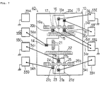
- Fig. 3 is a typical plan of a surface acoustic wave apparatus according to an embodiment of the present invention. An electrical connection structure of the apparatus will be described below.
- Fig. 4 is a longitudinal section of the surface acoustic wave apparatus.
- the surface acoustic wave apparatus includes first and second series-coupled resonator filters 11 and 12 having different pass-band characteristics.
- the first and second series-coupled resonator filters 11 and 12 are configured by forming various electrodes described later on a surface-wave board 13, and as a whole a single SAW filter chip 10 is formed.
- the surface-wave board 13 is made from a piezoelectric material such as piezoelectric single crystal, including LiTaO 3 , LiNbO 3 , and quartz crystal, and piezoelectric ceramic, including lead-titanate-zirconate piezoelectric ceramic.
- the surface-wave board 13 may be an insulating board, such as alumina, on which piezoelectric thin film, including ZnO, is formed. In this case, various electrodes described later are formed such that they contact piezoelectric thin film, in other words, on the piezoelectric thin film or between the piezoelectric thin film and the insulating board.
- the first and second series-coupled resonator filters 11 and 12 are formed such that the pass band of the first series-coupled resonator filter is 860 to 885 MHz and the pass band of the second series-coupled resonator filter is 810 to 828 MHz.
- an input electrode 14 is formed.
- the input electrode 14 is connected to the hot electrode of an IDT 16 disposed at the center of the first series-coupled resonator filter 11 through an impedance-matching IDT 15.
- the ground electrode of the IDT 16 is connected to an ground-electrode land 16a.
- IDTs 17 and 18 are formed at both sides of the IDT 16.
- Reflectors 19a and 19b are disposed at both sides of an area where IDTs 16 to 18 are formed in the direction in which a surface acoustic wave transmits.
- the hot electrodes of IDTs 17 and 18 are electrically connected to each other with an electrode pattern formed on the surface-wave board 13.
- An output-electrode land 20a is formed at a certain point in the electrode pattern.
- the hot electrodes of IDTs 17 and 18 are electrically connected to ground-electrode lands 20b and 20c, respectively.
- the ground electrode of the center IDT 16 and the ground-electrode land 16a are enclosed by the electrode pattern 20d which connects the hot electrodes of IDTs 17 and 18 in common.
- the second series-coupled resonator filter 12 is electrically connected to the input electrode 14 through impedance-matching resonators 21 and 22.
- a center IDT 23 serves as an output IDT
- IDTs 24 and 25 disposed at both sides of the IDT 23 serve as input IDTs.
- Reflectors 26a and 26b are formed at both sides of IDTs 23 to 25 in the direction in which a surface acoustic wave transmits.
- the hot electrode of IDT 23 is electrically connected to an output-electrode land 27a formed on the surface-wave board.
- An electrode connected to the ground of IDT 23 is connected to an ground-electrode land 27b.
- the ground electrodes of IDTs 24 and 25 disposed at both sides of IDT 23 are connected in common to a ground-electrode land 27c formed on the surface-wave board 13.
- the output-electrode land 27a is enclosed by an electrode pattern 27d which connects the ground electrodes of IDTs 24 and 25 in common.
- the hot electrodes of IDTs 24 and 25 are connected in common and further connected to the input electrode 14 described above.
- the ground-electrode land 27b is enclosed by an electrode pattern 27e connecting to the hot electrode of IDTs 24 and 25.
- the various electrodes are formed on the surface acoustic board 13, and the SAW filter chip 10 includes two-stage resonator filter having the input electrode 14 and the output-electrode lands 20a and 27a.
- the SAW filter chip 10 is accommodated into a package 30 as shown in Fig. 4.
- the package 30 includes a package member 31 formed of a multilayer board and a cover member 32 made of a metal.
- the package member 31 is formed by, for example, a ceramic lamination technology, and has electrodes 31a to 31c in its inside at a plurality of heights.
- Fig. 4 indicates the heights of electrodes 31a to 31c in a sketch manner. Electrodes 31a to 31c have various patterns. Electrode 31a serves as a ground pattern and is connected to external electrodes 31d and 31e at both ends. Electrode 31b indicates ground electrodes among electrodes 33A to 33H shown in Fig. 3 and described later.
- Electrodes 33A to 33H indicated at the sides of the SAW filter chip 10 in Fig. 3 are formed on the same layer of the package member. Electrode 33B serves as an input electrode, electrodes 33F and 33H serve as output electrodes, and the other electrodes 33A, 33C, 33D, 33E, and 33G serve as ground electrodes.
- the input electrode 14 of the surface acoustic wave filter chip 10 is electrically connected to an input electrode 33B formed in the package member, by bonding wire 34a.
- An output electrode 33F of the package member is connected to an output-electrode land 20a by bonding wire 34b.
- An output electrode 33H is electrically connected to an output-electrode land 27a of the second series-coupled resonator filter 12 by bonding wire 34c.
- ground electrode of IDT 17 which is one of the IDTs adjacent to the reflectors of the first series-coupled resonator filter 11, is connected to a ground-electrode land 20b.
- a ground-electrode land 20b is electrically connected to ground electrodes 33A and 33G by two bonding wires 34d and 34e.
- a ground-electrode land 20c connected to the ground electrode of IDT 18 is connected to a ground electrode 33G by bonding wire 34f.
- ground electrodes of IDTs 17 and 18 are connected to ground electrodes 33A and 33G formed in the package, by bonding wires 34d, 34e, and 34f. At least two bonding wires, 34d and 34e, are connected to different ground electrodes 33A and 33G. A third bonding wire 34f is connected between a ground-electrode land 20c and a ground electrode 33G.
- a ground-electrode land 16a connected to the hot electrode of the center IDT 16 is connected to a ground electrode 33E by bonding wire 34j.
- Ground electrodes 33A and 33G are electrically connected through ground patterns formed in different layers of the package.
- electrodes connected to the ground of IDTs 24 and 25 adjacent to the reflectors are connected to a ground-electrode land 27c.
- a ground-electrode land 27c is electrically connected to ground electrodes 33C and 33D with bonding wires 34g and 34h. In other words, at least two bonding wires 34g and 34h are connected to different ground electrodes 33C and 33D.
- a fourth bonding wire 34i is connected between a ground-electrode land 27b and a ground electrode 33C.
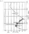
- Fig. 5 shows the frequency-amplitude characteristics of the first series-coupled resonator filter 11 at the inside and outside of the pass band in the surface acoustic wave filter apparatus according to the present embodiment shown in Figs. 3 and 4.
- Fig. 6 shows the frequency-amplitude characteristics of the second series-coupled resonator filter 12 at the inside and outside of the pass band.
- Figs. 8 and 9 show the frequency-amplitude characteristics of first and second series-coupled resonator filters 41 and 42 shown in Fig. 7, which constitute a surface acoustic wave filter apparatus.
- the surface acoustic wave filter apparatus 40 shown in Fig. 7 is the same as that shown in Fig. 3 except that neither bonding wire 34d nor bonding wire 34f, both shown in Fig. 3, is used. Therefore, the same reference numerals are assigned to the same portions and the descriptions thereof will be omitted.
- the surface acoustic wave filter apparatus 40 shown in Fig. 7 is the same as that described in the above embodiment except that the ground electrodes of both-side IDTs adjacent to the reflectors in the first and second series-coupled resonator filters are not connected to different ground electrodes of the package by at least two bonding wires.
- the surface acoustic wave filter apparatus of the present embodiment has larger attenuation at the outside of the pass band, especially at the higher-frequency side, for both the first and second series-coupled resonator filters than the surface acoustic wave filter apparatus shown in Fig. 7.
- Fig. 10 shows frequency-amplitude characteristics in a case in which ground terminals are independently connected to different ground electrodes formed in a package member at the input and output sides of a series-coupled resonator filter as described in Japanese Unexamined Patent Publication No. 4-263509.
- the same filter as the first series-coupled resonator filter 11 shown in Fig. 3 except for connection with bonding wire at the ground electrodes was made to obtain the characteristics shown in Fig. 10.
- the reasons why the surface acoustic wave filter apparatus of the present embodiment has a large attenuation outside the pass band as described above are that a residual inductance at portions from the ground terminals of the series-coupled resonator filter to the ground electrodes at the package side and a residual inductance at a ground pattern from the inside of the package to an external terminal are reduced, and a decrease in attenuation at the higher frequency side than the pass band is suppressed due to enhancement of the ground paths.
- parasitic capacitances are generated therebetween. It is preferred that these parasitic capacitances be small. It is preferred that the sides opposing the hot electrodes, of the ground electrodes of IDTs 16 and 23 be small. In contrast, the ground electrodes of outer IDTs 17 and 18 and IDTs 24 and 25 can have larger electrode areas without increasing their sides opposing the hot electrodes. Therefore, an increase in the above parasitic capacitances is small.
- the area of the electrode needs to be extended. It is preferred that the number of bonding wires be increased at the ground electrodes of outer IDTs in order to suppress an increase of parasitic capacitance. Therefore, in the present embodiment, since the number of bonding wires connected to the ground electrodes of outer IDTs 17, 18, 24, and 25 is increased as described above, an increase of the parasitic capacitance can be effectively suppressed.
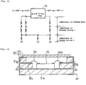
- Figs. 12 and 13 are a cross section and a partially broken plan in section used for describing a surface acoustic wave apparatus according to a second embodiment of the present invention.
- the surface acoustic wave apparatus of the present embodiment is configured in the same way as in the surface acoustic wave apparatus of the first embodiment except for the ground patterns formed in the package.
- the SAW filter chip 10 described in the first embodiment is accommodated into a package 30.
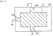
- the SAW filter chip 10 is secured on a ground pattern 41 formed on a ceramic layer 31e of a package member 31.
- the ground pattern 41 is formed on the upper surface of the ceramic layer 31e such that it has an almost rectangular shape smaller in area than the ceramic layer 31e, as shown in Fig. 13.
- the ground pattern 41 is led to peripheral edges of the ceramic layer 31e by lead sections 41a to 41c. In Fig. 13, the lead sections 41a to 41c separately reach three sides of the ceramic layer 31e.
- external electrodes 42 and 43 are formed at sides of the package member 31 such that they are electrically connected to ground electrodes 33C and 33E described before and also electrically connected to the ground pattern 41.
- the external electrodes 42 and 43 are joined to the cover member 32 made of a metal, at the upper surface of a ceramic layer 31g.
- ground electrodes 33A, 33D, and 33E are electrically connected to the external electrodes 42 and 43 in the same way as for ground electrodes 33C and 33G.
- the ground pattern 41 which is electrically joined to the cover member 32 made from a metal, is formed of internal wiring of the package member 31 made from ceramic, and is led at three portions as describe above, a sufficient case ground is obtained.
- Fig. 14 shows the frequency-amplitude characteristics of the first series-coupled resonator filter in the surface acoustic wave apparatus of the present embodiment. It is clear from comparison between the characteristics shown in Fig. 14 and that shown in Fig. 5, in which case grounding is obtained at two portions, that attenuation can further be increased at the higher frequency side than the pass band.
- the pass band of the first SAW resonator filter of the present embodiment is 860 to 885 MHz.
Landscapes
- Physics & Mathematics (AREA)
- Acoustics & Sound (AREA)
- Surface Acoustic Wave Elements And Circuit Networks Thereof (AREA)
Applications Claiming Priority (3)
| Application Number | Priority Date | Filing Date | Title |
|---|---|---|---|
| JP24518896 | 1996-09-17 | ||
| JP24518896A JP3227645B2 (ja) | 1996-09-17 | 1996-09-17 | 弾性表面波装置 |
| JP245188/96 | 1996-09-17 |
Publications (3)
| Publication Number | Publication Date |
|---|---|
| EP0829958A2 true EP0829958A2 (de) | 1998-03-18 |
| EP0829958A3 EP0829958A3 (de) | 2000-04-26 |
| EP0829958B1 EP0829958B1 (de) | 2005-11-30 |
Family
ID=17129933
Family Applications (1)
| Application Number | Title | Priority Date | Filing Date |
|---|---|---|---|
| EP97116175A Expired - Lifetime EP0829958B1 (de) | 1996-09-17 | 1997-09-17 | Akustische Oberflächenwellenvorrichtung |
Country Status (5)
| Country | Link |
|---|---|
| US (1) | US5966060A (de) |
| EP (1) | EP0829958B1 (de) |
| JP (1) | JP3227645B2 (de) |
| KR (1) | KR100278748B1 (de) |
| DE (1) | DE69734753T2 (de) |
Cited By (4)
| Publication number | Priority date | Publication date | Assignee | Title |
|---|---|---|---|---|
| EP0961404A3 (de) * | 1998-05-29 | 2000-08-09 | Fujitsu Limited | Akustisches Oberflächenwellenfilter mit verbesserter Unterdrückung ausserhalb eines Durchlassbereichs |
| EP1050961A2 (de) * | 1999-03-10 | 2000-11-08 | Murata Manufacturing Co., Ltd. | Akustisches Oberfächenwellenfilter und Kommunikationsgerät mit solch einem Filter |
| WO2001069782A1 (de) * | 2000-03-13 | 2001-09-20 | Epcos Ag | Duplexer mit verbesserter unterdrückung von harmonischen |
| EP2043263A1 (de) * | 1999-08-11 | 2009-04-01 | Fujitsu Media Devices Limited | Akustische Oberflächenwellenvorrichtung für Flip-Chip-Montage |
Families Citing this family (17)
| Publication number | Priority date | Publication date | Assignee | Title |
|---|---|---|---|---|
| JP3239064B2 (ja) * | 1996-05-28 | 2001-12-17 | 富士通株式会社 | 弾性表面波装置 |
| US6222426B1 (en) * | 1998-06-09 | 2001-04-24 | Oki Electric Industry, Co., Ltd. | Branching filter with a composite circuit of an LC circuit and a serial arm saw resonator |
| US6937113B2 (en) * | 1998-06-09 | 2005-08-30 | Oki Electric Industry Co., Ltd. | Branching filter package |
| JP2000059176A (ja) * | 1998-08-06 | 2000-02-25 | Toshiba Corp | 弾性表面波素子 |
| JP3382920B2 (ja) | 2000-06-30 | 2003-03-04 | 沖電気工業株式会社 | 共振器型弾性表面波フィルタ |
| JP3454239B2 (ja) * | 2000-08-31 | 2003-10-06 | 株式会社村田製作所 | 弾性表面波フィルタ |
| JP3780415B2 (ja) * | 2001-06-12 | 2006-05-31 | 株式会社村田製作所 | 縦結合共振子型弾性表面波フィルタ、およびそれを用いた通信機装置 |
| JP4726358B2 (ja) * | 2001-08-31 | 2011-07-20 | 京セラ株式会社 | 弾性表面波装置 |
| TWI315607B (en) * | 2001-10-29 | 2009-10-01 | Panasonic Corp | Surface acoustic wave filter element, surface acoustic wave filter and communication device using the same |
| JP3818896B2 (ja) * | 2001-11-26 | 2006-09-06 | 富士通メディアデバイス株式会社 | 分波器及びこれを用いた電子装置 |
| US6765456B2 (en) * | 2001-12-17 | 2004-07-20 | Oki Electric Industry Co., Ltd. | Surface acoustic wave duplexer and portable communication device using the same |
| JP3993579B2 (ja) | 2004-04-28 | 2007-10-17 | 富士通メディアデバイス株式会社 | バランス出力型フィルタ |
| JP4816710B2 (ja) * | 2008-10-30 | 2011-11-16 | 株式会社村田製作所 | 分波器 |
| DE102010005306B4 (de) | 2010-01-21 | 2015-06-18 | Epcos Ag | DMS Filter mit verbesserter Signalunterdrückung |
| JP5890670B2 (ja) | 2011-12-05 | 2016-03-22 | 太陽誘電株式会社 | フィルタ及び分波器 |
| CN112367059B (zh) * | 2020-11-25 | 2024-05-17 | 重庆邮电大学 | 一种声表面波滤波器的封装键合线等效电路模型 |
| CN121567087B (zh) * | 2026-01-22 | 2026-04-24 | 天通瑞宏科技有限公司 | 一种声表面波谐振器、声表面波滤波器及多工器 |
Family Cites Families (9)
| Publication number | Priority date | Publication date | Assignee | Title |
|---|---|---|---|---|
| US4365219A (en) * | 1981-02-27 | 1982-12-21 | General Electric Company | In-line surface acoustic wave filter assembly module and method of making same |
| JPH03284006A (ja) * | 1990-03-30 | 1991-12-13 | Fujitsu Ltd | 弾性表面波デバイス |
| JPH0555872A (ja) * | 1991-08-21 | 1993-03-05 | Toyo Commun Equip Co Ltd | 二段縦続接続二重モードsawフイルタ |
| JPH06152313A (ja) * | 1992-10-30 | 1994-05-31 | Japan Energy Corp | 弾性表面波フィルタ |
| JP3379775B2 (ja) * | 1992-11-17 | 2003-02-24 | 富士通株式会社 | 弾性表面波フィルタ |
| DE69423062T2 (de) * | 1993-08-06 | 2000-06-29 | Kinseki, Ltd. | Akustische Oberflächenwellenanordnung |
| JP2905094B2 (ja) * | 1994-07-01 | 1999-06-14 | 富士通株式会社 | 分波器パッケージ |
| WO1996015587A1 (en) * | 1994-11-10 | 1996-05-23 | Fujitsu Limited | Acoustic wave filter |
| JP3350609B2 (ja) * | 1995-03-24 | 2002-11-25 | ティーディーケイ株式会社 | 弾性表面波装置 |
-
1996
- 1996-09-17 JP JP24518896A patent/JP3227645B2/ja not_active Expired - Lifetime
-
1997
- 1997-09-16 US US08/931,566 patent/US5966060A/en not_active Expired - Lifetime
- 1997-09-17 DE DE69734753T patent/DE69734753T2/de not_active Expired - Lifetime
- 1997-09-17 EP EP97116175A patent/EP0829958B1/de not_active Expired - Lifetime
- 1997-09-18 KR KR1019970047617A patent/KR100278748B1/ko not_active Expired - Lifetime
Cited By (5)
| Publication number | Priority date | Publication date | Assignee | Title |
|---|---|---|---|---|
| EP0961404A3 (de) * | 1998-05-29 | 2000-08-09 | Fujitsu Limited | Akustisches Oberflächenwellenfilter mit verbesserter Unterdrückung ausserhalb eines Durchlassbereichs |
| US6388545B1 (en) | 1998-05-29 | 2002-05-14 | Fujitsu Limited | Surface-acoustic-wave filter having an improved suppression outside a pass-band |
| EP1050961A2 (de) * | 1999-03-10 | 2000-11-08 | Murata Manufacturing Co., Ltd. | Akustisches Oberfächenwellenfilter und Kommunikationsgerät mit solch einem Filter |
| EP2043263A1 (de) * | 1999-08-11 | 2009-04-01 | Fujitsu Media Devices Limited | Akustische Oberflächenwellenvorrichtung für Flip-Chip-Montage |
| WO2001069782A1 (de) * | 2000-03-13 | 2001-09-20 | Epcos Ag | Duplexer mit verbesserter unterdrückung von harmonischen |
Also Published As
| Publication number | Publication date |
|---|---|
| DE69734753T2 (de) | 2006-06-08 |
| DE69734753D1 (de) | 2006-01-05 |
| JP3227645B2 (ja) | 2001-11-12 |
| KR100278748B1 (ko) | 2001-01-15 |
| US5966060A (en) | 1999-10-12 |
| EP0829958A3 (de) | 2000-04-26 |
| KR19980024722A (ko) | 1998-07-06 |
| JPH1093381A (ja) | 1998-04-10 |
| EP0829958B1 (de) | 2005-11-30 |
Similar Documents
| Publication | Publication Date | Title |
|---|---|---|
| EP0829958B1 (de) | Akustische Oberflächenwellenvorrichtung | |
| US6417574B1 (en) | Surface-acoustic-wave device for flip-chip mounting | |
| US6919777B2 (en) | Surface acoustic wave filter device | |
| US6566981B2 (en) | Surface acoustic wave device having plural ground conductor films in the housing cavity | |
| US6943645B2 (en) | Surface acoustic wave duplexer and communication apparatus having the same | |
| EP2501039B1 (de) | Oberflächenwelleneinrichtung und Rand-Oberflächenwelleneinrichtung | |
| US7479846B2 (en) | Duplexer | |
| US8179211B2 (en) | RF-filter with improved adjacent channel suppression | |
| JP6651643B2 (ja) | 弾性波フィルタ、分波器および通信装置 | |
| EP1296454B1 (de) | Akustisches Oberflächenwellenelement und akustische Oberflächenwellenvorrichtung | |
| KR100280611B1 (ko) | 탄성표면파장치 | |
| US20060139125A1 (en) | Filter device | |
| EP1675262B1 (de) | Duplexer | |
| JP7620319B2 (ja) | 弾性波デバイスチップ、弾性波デバイスおよびその弾性波デバイスチップまたは弾性波デバイスを備えるモジュール | |
| KR20060040726A (ko) | 탄성 표면파 디바이스 | |
| JP7347956B2 (ja) | 高周波デバイスおよびマルチプレクサ | |
| US20240364308A1 (en) | Composite filter device | |
| JP3948550B2 (ja) | 弾性表面波装置 | |
| JP3697308B2 (ja) | 弾性表面波装置 | |
| JP3198489B2 (ja) | フィルタ用パッケージ | |
| US20260066877A1 (en) | Composite filter device | |
| US20240364310A1 (en) | Acoustic wave devices and modules with acoustic wave devices | |
| JP2025149117A (ja) | フィルタ及びマルチプレクサ | |
| WO2023248823A1 (ja) | フィルタデバイス、多層基板及び通信装置 | |
| JP2000164744A (ja) | 表面波デバイスとそのパッケージ |
Legal Events
| Date | Code | Title | Description |
|---|---|---|---|
| PUAI | Public reference made under article 153(3) epc to a published international application that has entered the european phase |
Free format text: ORIGINAL CODE: 0009012 |
|
| AK | Designated contracting states |
Kind code of ref document: A2 Designated state(s): DE FI FR GB IT NL SE |
|
| PUAL | Search report despatched |
Free format text: ORIGINAL CODE: 0009013 |
|
| AK | Designated contracting states |
Kind code of ref document: A3 Designated state(s): AT BE CH DE DK ES FI FR GB GR IE IT LI LU MC NL PT SE |
|
| 17P | Request for examination filed |
Effective date: 20000524 |
|
| AKX | Designation fees paid |
Free format text: DE FI FR GB IT NL SE |
|
| 17Q | First examination report despatched |
Effective date: 20041126 |
|
| GRAP | Despatch of communication of intention to grant a patent |
Free format text: ORIGINAL CODE: EPIDOSNIGR1 |
|
| GRAS | Grant fee paid |
Free format text: ORIGINAL CODE: EPIDOSNIGR3 |
|
| GRAA | (expected) grant |
Free format text: ORIGINAL CODE: 0009210 |
|
| AK | Designated contracting states |
Kind code of ref document: B1 Designated state(s): DE FI FR GB IT NL SE |
|
| PG25 | Lapsed in a contracting state [announced via postgrant information from national office to epo] |
Ref country code: NL Free format text: LAPSE BECAUSE OF FAILURE TO SUBMIT A TRANSLATION OF THE DESCRIPTION OR TO PAY THE FEE WITHIN THE PRESCRIBED TIME-LIMIT Effective date: 20051130 Ref country code: IT Free format text: LAPSE BECAUSE OF FAILURE TO SUBMIT A TRANSLATION OF THE DESCRIPTION OR TO PAY THE FEE WITHIN THE PRESCRIBED TIME-LIMIT;WARNING: LAPSES OF ITALIAN PATENTS WITH EFFECTIVE DATE BEFORE 2007 MAY HAVE OCCURRED AT ANY TIME BEFORE 2007. THE CORRECT EFFECTIVE DATE MAY BE DIFFERENT FROM THE ONE RECORDED. Effective date: 20051130 Ref country code: FI Free format text: LAPSE BECAUSE OF FAILURE TO SUBMIT A TRANSLATION OF THE DESCRIPTION OR TO PAY THE FEE WITHIN THE PRESCRIBED TIME-LIMIT Effective date: 20051130 |
|
| REG | Reference to a national code |
Ref country code: GB Ref legal event code: FG4D |
|
| REF | Corresponds to: |
Ref document number: 69734753 Country of ref document: DE Date of ref document: 20060105 Kind code of ref document: P |
|
| PG25 | Lapsed in a contracting state [announced via postgrant information from national office to epo] |
Ref country code: SE Free format text: LAPSE BECAUSE OF FAILURE TO SUBMIT A TRANSLATION OF THE DESCRIPTION OR TO PAY THE FEE WITHIN THE PRESCRIBED TIME-LIMIT Effective date: 20060228 |
|
| NLV1 | Nl: lapsed or annulled due to failure to fulfill the requirements of art. 29p and 29m of the patents act | ||
| PLBE | No opposition filed within time limit |
Free format text: ORIGINAL CODE: 0009261 |
|
| STAA | Information on the status of an ep patent application or granted ep patent |
Free format text: STATUS: NO OPPOSITION FILED WITHIN TIME LIMIT |
|
| 26N | No opposition filed |
Effective date: 20060831 |
|
| EN | Fr: translation not filed | ||
| GBPC | Gb: european patent ceased through non-payment of renewal fee |
Effective date: 20060917 |
|
| PG25 | Lapsed in a contracting state [announced via postgrant information from national office to epo] |
Ref country code: GB Free format text: LAPSE BECAUSE OF NON-PAYMENT OF DUE FEES Effective date: 20060917 |
|
| PG25 | Lapsed in a contracting state [announced via postgrant information from national office to epo] |
Ref country code: FR Free format text: LAPSE BECAUSE OF FAILURE TO SUBMIT A TRANSLATION OF THE DESCRIPTION OR TO PAY THE FEE WITHIN THE PRESCRIBED TIME-LIMIT Effective date: 20070119 |
|
| PG25 | Lapsed in a contracting state [announced via postgrant information from national office to epo] |
Ref country code: FR Free format text: LAPSE BECAUSE OF FAILURE TO SUBMIT A TRANSLATION OF THE DESCRIPTION OR TO PAY THE FEE WITHIN THE PRESCRIBED TIME-LIMIT Effective date: 20051130 |
|
| PGFP | Annual fee paid to national office [announced via postgrant information from national office to epo] |
Ref country code: DE Payment date: 20160921 Year of fee payment: 20 |
|
| REG | Reference to a national code |
Ref country code: DE Ref legal event code: R071 Ref document number: 69734753 Country of ref document: DE |