EP0833377B1 - Hydrogénation ameliorée pour materiaux encapsulés par un oxyde - Google Patents
Hydrogénation ameliorée pour materiaux encapsulés par un oxyde Download PDFInfo
- Publication number
- EP0833377B1 EP0833377B1 EP97307393.5A EP97307393A EP0833377B1 EP 0833377 B1 EP0833377 B1 EP 0833377B1 EP 97307393 A EP97307393 A EP 97307393A EP 0833377 B1 EP0833377 B1 EP 0833377B1
- Authority
- EP
- European Patent Office
- Prior art keywords
- oxide
- poly
- hydrogenation
- layer
- hydrogen
- Prior art date
- Legal status (The legal status is an assumption and is not a legal conclusion. Google has not performed a legal analysis and makes no representation as to the accuracy of the status listed.)
- Expired - Lifetime
Links
Images


Classifications
-
- H—ELECTRICITY
- H10—SEMICONDUCTOR DEVICES; ELECTRIC SOLID-STATE DEVICES NOT OTHERWISE PROVIDED FOR
- H10P—GENERIC PROCESSES OR APPARATUS FOR THE MANUFACTURE OR TREATMENT OF DEVICES COVERED BY CLASS H10
- H10P95/00—Generic processes or apparatus for manufacture or treatments not covered by the other groups of this subclass
- H10P95/94—Hydrogenation or deuterisation, e.g. using atomic hydrogen from a plasma
-
- Y—GENERAL TAGGING OF NEW TECHNOLOGICAL DEVELOPMENTS; GENERAL TAGGING OF CROSS-SECTIONAL TECHNOLOGIES SPANNING OVER SEVERAL SECTIONS OF THE IPC; TECHNICAL SUBJECTS COVERED BY FORMER USPC CROSS-REFERENCE ART COLLECTIONS [XRACs] AND DIGESTS
- Y10—TECHNICAL SUBJECTS COVERED BY FORMER USPC
- Y10S—TECHNICAL SUBJECTS COVERED BY FORMER USPC CROSS-REFERENCE ART COLLECTIONS [XRACs] AND DIGESTS
- Y10S438/00—Semiconductor device manufacturing: process
- Y10S438/958—Passivation layer
Definitions
- the present invention is directed to the hydrogenation of oxide-coated materials such as polycrystalline silicon films and devices using a surface coating with low reflectivity of monatomic hydrogen.
- Polycrystalline silicon films are used in a wide variety of devices.
- poly-Si is used in numerous applications including, but not limited to, thin-film transistors, solar cells, liquid-crystal displays, printers, scanners, and the like.
- the poly-Si layer is encapsulated by an oxide or oxy-nitride film.
- passivate dopants such as boron, phosphorous, and the like (i.e., hydrogenation of boron doped single or polycrystalline silicon encapsulated by an oxide).
- a method according to the present invention comprises the features defined in claim 1. Embodiments comprise the features defined in the dependent claims.
- the present invention is directed to a process for the enhancement of hydrogenation of oxide-encapsulated materials.
- the present invention results in a significant decrease in the hydrogenation time required to passivate such oxide-coated materials.
- a poly-Si material such as a poly-Si film or device is encapsulated by an oxide and coated with an injection layer having low reflectivity of monatomic hydrogen.
- the material may be encapsulated with an oxide by thermal wet or dry oxide growth, implantation of oxygen into the material, sputtering, deposition, and the like.
- the oxide-encapsulated layer includes, but is not limited to, SiO x , wherein 1 ⁇ x ⁇ 2. The thickness of the oxide layer is sufficient if it is continuous and has no pin holes. However, hydrogen passivation is inhibited. The present invention overcomes this problem.
- Hydrogen concentration profiles in oxides generally cannot be measured accurately by secondary ion mass spectrometry ("SIMS”) because of charging of the substrate during sputtering of the oxide layer.
- SIMS secondary ion mass spectrometry
- the underlying material such as a poly-Si substrate, can be used as a detector.
- deuterium is used because it is a readily identifiable isotope that duplicates hydrogen chemistry.
- D is used to analyze the hydrogenation according to the present invention.
- hydrogen is preferably used in embodiments of the present invention.
- the poly-Si substrate collects the D passing through the oxide and other layers or barriers.
- the deuterium trapped in the poly-Si substrate is measured using SIMS after the oxide layer is removed.
- the deuterium, and thus hydrogen, diffusion through the oxide layer is studied by measuring the changes of the D flux through the oxide as a function of hydrogenation time, substrate temperature and oxide thickness.
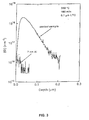
- Figure 1 shows the influence of an oxide layer on the hydrogenation of a poly-Si film.
- a solid state crystallized poly-Si film with a densified low temperature oxide (“LTO") layer of about 3.0 ⁇ m thickness on top is exposed to monatomic deuterium in an optically isolated remote hydrogen microwave plasma at 350°C for 180 minutes.
- the LTO layer is removed from the poly-Si film with hydrogen fluoride, HF.
- a poly-Si film without a LTO layer is exposed to monatomic deuterium in a hydrogen plasma at 350°C for 30 minutes.
- the D concentration profiles for both the coated and uncoated poly-Si films are measured by SIMS.
- a remote hydrogenation system may be used to expose poly-Si films to monatomic deuterium.
- regular plasma hydrogenators and electron cyclotron resonance (ECR) machines may also be employed in other embodiments.
- ECR electron cyclotron resonance
- the physical limitation of hydrogen passivation is the oxide layer, not the method used to generate the H atoms.
- the temperature range for hydrogenation may be between about 200°C and about 500°C.
- the time for hydrogenation can be any time suitable to passivate the underlying oxide-encapsulated material. In embodiments, the period of time for hydrogenation is from about 30 minutes to about 180 minutes. A plot of the number of passivated spins as a function of time and temperature appears in Nickel et al., 62 Appl. Phys. Lett. 3285 (1993 ).
- the hydrogen gas, H 2 pressure can be any suitable pressure to passivate the underlying oxide-encapsulated material to achieve the objects of the present invention. Preferably, in embodiments, the pressure is about 2.0 Torr.
- Figure 1 shows a reduction of the total D flux into the poly-Si due to the presence of the oxide.
- comparably low D concentrations and depth profiles are also obtained when the LTO layer is only 0.3 ⁇ m thick as demonstrated in Nickel et al., 52 Phys. Rev. B, 7791 (1995 ).
- the D concentrations in the poly-Si films are integrated and divided by the hydrogenation time to obtain the average flux.
- the low D flux into the underlying poly-Si film is due to a significant barrier for atomic D or H entering the oxide layer and is not limited by the D or H diffusivity in the oxide.
- a coating i.e., injection layer
- low reflectivity means that H or D atoms hitting the coated SiO x surface enter the injection layer, and subsequently the oxide, and are not reflected back into an atomic hydrogen source, such as a hydrogen plasma.
- the coating may be deposited by any of the various suitable methods, such as evaporation, sputtering, chemical vapor deposition, molecular beam epitaxy, metallo-organic chemical vapor deposition, and the like.
- the deposited capping layer may include a metal based layer. The metal must not be easily oxidized.
- Hydrogen prefers metals with a high electron concentration. Hydrogen diffusion from such a metal into an oxide is enhanced for metals with a low H solubility. When using a metal or silicon-based injection layer, hydrogen that diffuses into the injection layer exits primarily through the oxide layer. Thus, according to the present invention, diffusion into the oxide is increased, as is hydrogenation of the underlying material.
- the deposited injection layer comprises gold (Au).
- the deposited coating is of a suitable thickness, preferably in a layer of from about 5 nm to about 7 nm. Although the thickness of the injection layer is not particularly limited, a thin and continuous coating is necessary. A thick coating may increase hydrogenation time and thus passivation time.
- the time for the hydrogenation of oxide-encapsulated materials such as poly-Si films and devices is substantially reduced.
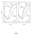
- the electrical transfer characteristics of poly-Si thin-film transistors are improved, as shown in Table 1 and Figure 4 , described in more detail below.
- a poly-Si film with a 3.0 ⁇ m LTO layer is covered with 5 nm of Au.
- the oxide-coated poly-Si film with the Au injection layer and a control example, a poly-Si film encapsulated by a 3.0 ⁇ m thick layer of LTO, are simultaneously exposed to monatomic deuterium generated in an optically isolated remote microwave plasma at 350°C for 180 minutes.
- Figure 2 shows the deuterium concentration profiles of the oxide-encapsulated film with an Au injection layer and the control example. A striking increase of the D concentration in the poly-Si is observed due to the presence of the Au injection layer.
- the D concentration at the surface of the poly-Si film increases by a factor of about 75 when the LTO is coated with Au. Moreover, D is traced to a depth of about 0.2 ⁇ m in the poly-Si film.
- an Au injection layer lowers the surface barrier of the LTO and enhances the hydrogenation efficiency of a poly-Si film or device.
- Figure 2 demonstrates that Pt enhances the diffusion of D into the poly-Si film.
- the D concentration is only enhanced close to the poly-Si surface, indicating that Pt lowers the barrier for H incorporation.
- the lower passivation efficiency is due to the position of the hydrogen chemical potential (m H ) in the metal.
- m H has to be increased by filling empty states in the Pt layer with H.
- a time delay of the H emission into the LTO layer occurs when using a Pt injection layer as compared to an Au injection layer.
- the Al-capped, oxide-encapsulated poly-Si film and the control sample are simultaneously exposed to monatomic D at 350°C for 180 minutes.
- the metal and silicon oxide layers are removed with HF prior to SIMS measurements. From Figure 3 , it can be seen that Al does not lower the oxide surface barrier for D incorporation.
- Metals that form an insulating oxide layer such as Al, which forms Al 2 O 3 , can prevent H atoms from entering the metal and thereby effectively prevent the H passivation process of subsequent layers.
- Top-gate poly-Si thin-film transistor (“TFT”) chips encapsulated by a 3.0 ⁇ m thick silicon oxide layer are coated with 5 nm Au and 7 nm a-Si:H, respectively.
- the thin-film transistors are hydrogenated at 350°C for 30 minutes.
- control samples of similar TFT chips are prepared but without the injection layer.
- the electrical transfer characteristics prior to and after hydrogenation are shown in Figure 4 and in Table 1 below.
- the thin-film transistor chips with the Au and a-Si:H injection layers on top of the LTO exhibit an improved transfer characteristic with respect to the control samples.
- the pre-threshold slopes improve, the threshold voltages are smaller and the ON currents are higher than the control examples (oxide-encapsulated TFT chips without an injection layer).
- the pre-threshold slopes of all I SD -V G curves are summarized in Table 1, in which I SD is the source to drain current and V G is the gate voltage.
- the source to drain voltage, V SD is 5 volts.
Landscapes
- Silicon Compounds (AREA)
- Thin Film Transistor (AREA)
- Organic Low-Molecular-Weight Compounds And Preparation Thereof (AREA)
- Physical Or Chemical Processes And Apparatus (AREA)
Claims (8)
- Procédé d'amélioration de l'hydrogénation d'un matériau encapsulé par un oxyde, comprenant :la formation d'une couche d'injection ayant une faible réflectivité de l'hydrogène monoatomique sur un matériau encapsulé par un oxyde ; etl'hydrogénation dudit matériau avec une source d'hydrogène atomique, dans lequel l'hydrogène est incorporé dans ledit matériau ;caractérisé en ce que ladite couche d'injection est de l'or.
- Procédé d'amélioration de l'hydrogénation selon la revendication 1, dans lequel ledit matériau est choisi dans le groupe constitué de GaN, C60, poly-diamant, diamant et silicium polycristallin.
- Procédé d'amélioration de l'hydrogénation selon l'une ou l'autre des revendications 1 ou 2, dans lequel le dioxyde est constitué d'un oxyde représenté par la formule SiOx, dans laquelle 1 ≤ x ≤ 2.
- Procédé d'amélioration de l'hydrogénation selon l'une quelconque des revendications 1 à 3, dans lequel ladite couche d'injection a une épaisseur comprise entre environ 5 et environ 7 nm.
- Procédé d'amélioration de l'hydrogénation selon l'une quelconque des revendications 1 à 4, dans lequel ladite couche d'injection est déposée par évaporation, pulvérisation, dépôt chimique en phase vapeur, épitaxie par faisceau moléculaire ou dépôt chimique en phase vapeur d'organo-métallique.
- Procédé d'amélioration de l'hydrogénation selon l'une quelconque des revendications 1 à 5, dans lequel ladite hydrogénation se produit à des températures comprises entre environ 200 °C et environ 500 °C.
- Procédé d'amélioration de l'hydrogénation selon l'une quelconque des revendications 1 à 6, dans lequel ladite hydrogénation est effectuée pendant une durée allant d'environ 30 minutes à environ 180 minutes.
- Procédé d'amélioration de l'hydrogénation selon la revendication 2, dans lequel ledit matériau est du silicium polycristallin.
Applications Claiming Priority (2)
| Application Number | Priority Date | Filing Date | Title |
|---|---|---|---|
| US723749 | 1996-09-30 | ||
| US08/723,749 US5744202A (en) | 1996-09-30 | 1996-09-30 | Enhancement of hydrogenation of materials encapsulated by an oxide |
Publications (3)
| Publication Number | Publication Date |
|---|---|
| EP0833377A2 EP0833377A2 (fr) | 1998-04-01 |
| EP0833377A3 EP0833377A3 (fr) | 1999-08-18 |
| EP0833377B1 true EP0833377B1 (fr) | 2016-01-13 |
Family
ID=24907508
Family Applications (1)
| Application Number | Title | Priority Date | Filing Date |
|---|---|---|---|
| EP97307393.5A Expired - Lifetime EP0833377B1 (fr) | 1996-09-30 | 1997-09-22 | Hydrogénation ameliorée pour materiaux encapsulés par un oxyde |
Country Status (3)
| Country | Link |
|---|---|
| US (1) | US5744202A (fr) |
| EP (1) | EP0833377B1 (fr) |
| JP (2) | JPH10120413A (fr) |
Families Citing this family (11)
| Publication number | Priority date | Publication date | Assignee | Title |
|---|---|---|---|---|
| KR910003742B1 (ko) * | 1986-09-09 | 1991-06-10 | 세미콘덕터 에너지 라보라터리 캄파니 리미티드 | Cvd장치 |
| US5872387A (en) * | 1996-01-16 | 1999-02-16 | The Board Of Trustees Of The University Of Illinois | Deuterium-treated semiconductor devices |
| US6252270B1 (en) * | 1997-04-28 | 2001-06-26 | Agere Systems Guardian Corp. | Increased cycle specification for floating-gate and method of manufacture thereof |
| US5982020A (en) | 1997-04-28 | 1999-11-09 | Lucent Technologies Inc. | Deuterated bipolar transistor and method of manufacture thereof |
| US6057182A (en) * | 1997-09-05 | 2000-05-02 | Sarnoff Corporation | Hydrogenation of polysilicon thin film transistors |
| US6143631A (en) * | 1998-05-04 | 2000-11-07 | Micron Technology, Inc. | Method for controlling the morphology of deposited silicon on a silicon dioxide substrate and semiconductor devices incorporating such deposited silicon |
| US6028015A (en) * | 1999-03-29 | 2000-02-22 | Lsi Logic Corporation | Process for treating damaged surfaces of low dielectric constant organo silicon oxide insulation material to inhibit moisture absorption |
| US6365511B1 (en) | 1999-06-03 | 2002-04-02 | Agere Systems Guardian Corp. | Tungsten silicide nitride as a barrier for high temperature anneals to improve hot carrier reliability |
| JPWO2003056622A1 (ja) * | 2001-12-26 | 2005-05-12 | 東京エレクトロン株式会社 | 基板処理方法および半導体装置の製造方法 |
| CN103985637B (zh) * | 2014-04-30 | 2017-02-01 | 京东方科技集团股份有限公司 | 低温多晶硅薄膜晶体管及其制作方法和显示装置 |
| US9698339B1 (en) | 2015-12-29 | 2017-07-04 | International Business Machines Corporation | Magnetic tunnel junction encapsulation using hydrogenated amorphous semiconductor material |
Family Cites Families (23)
| Publication number | Priority date | Publication date | Assignee | Title |
|---|---|---|---|---|
| US3442701A (en) * | 1965-05-19 | 1969-05-06 | Bell Telephone Labor Inc | Method of fabricating semiconductor contacts |
| US3849204A (en) * | 1973-06-29 | 1974-11-19 | Ibm | Process for the elimination of interface states in mios structures |
| US4359367A (en) * | 1980-06-25 | 1982-11-16 | Governing Council Of The University Of Toronto | Silicon-based semiconductor devices |
| GB2140202A (en) * | 1983-05-16 | 1984-11-21 | Philips Electronic Associated | Methods of manufacturing semiconductor devices |
| JPH0783031B2 (ja) * | 1984-03-08 | 1995-09-06 | 敏和 須田 | ▲ii▼−▲v▼族化合物半導体の薄膜又は結晶の製造方法 |
| FR2604828B1 (fr) * | 1986-10-06 | 1988-12-23 | Centre Nat Rech Scient | Procede de fabrication d'une diode p+nn+ et d'un transistor bipolaire comportant cette diode, utilisant l'effet de neutralisation des atomes donneurs par l'hydrogene atomique |
| US4857976A (en) * | 1987-06-30 | 1989-08-15 | California Institute Of Technology | Hydrogen-stabilized semiconductor devices |
| US4960675A (en) * | 1988-08-08 | 1990-10-02 | Midwest Research Institute | Hydrogen ion microlithography |
| FR2635611B1 (fr) * | 1988-08-18 | 1990-10-19 | Centre Nat Rech Scient | Procede de neutralisation des atomes accepteurs dans inp de type p |
| JPH02187037A (ja) * | 1989-01-13 | 1990-07-23 | Ricoh Co Ltd | 半導体層の水素化処理方法 |
| JP2770544B2 (ja) * | 1990-03-23 | 1998-07-02 | 松下電器産業株式会社 | Mis型半導体装置の製造方法 |
| US5225366A (en) * | 1990-06-22 | 1993-07-06 | The United States Of America As Represented By The Secretary Of The Navy | Apparatus for and a method of growing thin films of elemental semiconductors |
| DE69228868D1 (de) * | 1991-01-30 | 1999-05-12 | Minnesota Mining & Mfg | Verfahren zur Herstellung eines Polysilizium-Dünnfilmtransistors |
| US5483096A (en) * | 1991-11-07 | 1996-01-09 | Seiko Instruments Inc. | Photo sensor |
| US5194349A (en) * | 1992-02-07 | 1993-03-16 | Midwest Research Institute | Erasable, multiple level logic optical memory disk |
| US5250444A (en) * | 1992-02-21 | 1993-10-05 | North American Philips Corporation | Rapid plasma hydrogenation process for polysilicon MOSFETs |
| JPH05229966A (ja) * | 1992-02-25 | 1993-09-07 | Idemitsu Kosan Co Ltd | 水素化フラーレンの製造法 |
| EP0634797B1 (fr) * | 1993-07-13 | 1999-09-22 | Sony Corporation | Dispositif semi-conducteur à couche mince pour panneau à matrice active et sa méthode de fabrication |
| ZA946002B (en) * | 1993-08-12 | 1995-03-14 | De Beers Ind Diamond | Detecting ionising radiation |
| JP3338182B2 (ja) * | 1994-02-28 | 2002-10-28 | 株式会社半導体エネルギー研究所 | 半導体装置の作製方法 |
| US5620906A (en) * | 1994-02-28 | 1997-04-15 | Semiconductor Energy Laboratory Co., Ltd. | Method for producing semiconductor device by introducing hydrogen ions |
| JP3853395B2 (ja) * | 1994-03-27 | 2006-12-06 | 株式会社半導体エネルギー研究所 | 薄膜トランジスタの作製方法 |
| US5616933A (en) * | 1995-10-16 | 1997-04-01 | Sony Corporation | Nitride encapsulated thin film transistor fabrication technique |
-
1996
- 1996-09-30 US US08/723,749 patent/US5744202A/en not_active Expired - Lifetime
-
1997
- 1997-09-22 EP EP97307393.5A patent/EP0833377B1/fr not_active Expired - Lifetime
- 1997-09-30 JP JP9266852A patent/JPH10120413A/ja not_active Withdrawn
-
2009
- 2009-02-18 JP JP2009035040A patent/JP5320100B2/ja not_active Expired - Lifetime
Also Published As
| Publication number | Publication date |
|---|---|
| JP2009120482A (ja) | 2009-06-04 |
| JP5320100B2 (ja) | 2013-10-23 |
| EP0833377A2 (fr) | 1998-04-01 |
| JPH10120413A (ja) | 1998-05-12 |
| US5744202A (en) | 1998-04-28 |
| EP0833377A3 (fr) | 1999-08-18 |
Similar Documents
| Publication | Publication Date | Title |
|---|---|---|
| JP5320100B2 (ja) | 酸化物カプセル化材料の水素化の強化方法 | |
| EP0569470B1 (fr) | Procédé de fabrication d'un transistor à couche mince de polysilicium | |
| CA1283490C (fr) | Methode de passivation de la surface d'un semiconducteur compose et dispositif a interface semiconducteur-isolant amelioree | |
| US5387530A (en) | Threshold optimization for soi transistors through use of negative charge in the gate oxide | |
| US6613677B1 (en) | Long range ordered semiconductor interface phase and oxides | |
| US7795121B2 (en) | Method for manufacturing semiconductor device | |
| WO1995032519A1 (fr) | Procede de passivation a basse temperature d'objets de silicium permettant d'obtenir une faible densite d'etat d'interface | |
| US3853496A (en) | Method of making a metal insulator silicon field effect transistor (mis-fet) memory device and the product | |
| Okamura et al. | AlN capped annealing of Si implanted semi‐insulating GaAs | |
| Batey et al. | Plasma-enhanced CVD of high quality insulating films | |
| Fukumoto et al. | Electrical characteristics of metal‐insulator‐semiconductor diodes with ZrO2/SiO2 dielectric films | |
| Shimaya et al. | Electron Beam Induced Damage in Poly‐Si Gate MOS Structures and Its Effect on Long‐Term Stability | |
| EP0975013A2 (fr) | Méthode de fabrication d'une couche d'oxide sur un corps semiconducteur à base d' AsGa | |
| WO2003063227A2 (fr) | Procede de passivation de la surface d'un semi-conducteur iii-v | |
| US5972782A (en) | Ultrasound treatment of polycrystalline silicon thin films to enhance hydrogenation | |
| Mitani et al. | A study of the effect of deuterium on stress-induced leakage current | |
| Nishioka et al. | Time-dependent evolution of interface traps in hot-electron damaged metal/SiO 2/Si capacitors | |
| Kassabov et al. | Plasma processing effects on O2-HCl grown Si-SiO2 structures | |
| Haberle et al. | Electrical properties and structure of boron-doped sputter-deposited polycrystalline silicon films | |
| Haberle et al. | MOS device fabrication using sputter-deposited gate oxide and polycrystalline silicon layers | |
| El-Oyoun et al. | Structural properties of ultrathin amorphous silicon oxynitride layers | |
| Jackson et al. | Kinetics of carrier-induced metastable defect formation in hydrogenated amorphous silicon | |
| Majamaa | Ultrahigh vacuum plasma oxidation in the fabrication of ultrathin silicon dioxide films | |
| Chou et al. | Enhanced phosphorus diffusion during the glow discharge deposition of n‐type amorphous silicon hydrogen alloy | |
| Ohkawa et al. | Improving the reliability and the insulation properties of gate oxide in the gate injection mode by using a new procedure of (100) Si surface and Si/SiO/sub 2/interface treatments |
Legal Events
| Date | Code | Title | Description |
|---|---|---|---|
| PUAI | Public reference made under article 153(3) epc to a published international application that has entered the european phase |
Free format text: ORIGINAL CODE: 0009012 |
|
| AK | Designated contracting states |
Kind code of ref document: A2 Designated state(s): DE FR GB |
|
| PUAL | Search report despatched |
Free format text: ORIGINAL CODE: 0009013 |
|
| AK | Designated contracting states |
Kind code of ref document: A3 Designated state(s): AT BE CH DE DK ES FI FR GB GR IE IT LI LU MC NL PT SE |
|
| RIC1 | Information provided on ipc code assigned before grant |
Free format text: 6H 01L 21/30 A, 6H 01L 21/324 B |
|
| 17P | Request for examination filed |
Effective date: 20000218 |
|
| AKX | Designation fees paid |
Free format text: DE FR GB |
|
| 17Q | First examination report despatched |
Effective date: 20070619 |
|
| RAP1 | Party data changed (applicant data changed or rights of an application transferred) |
Owner name: THOMSON LICENSING LLC |
|
| RAP1 | Party data changed (applicant data changed or rights of an application transferred) |
Owner name: THOMSON LICENSING |
|
| GRAP | Despatch of communication of intention to grant a patent |
Free format text: ORIGINAL CODE: EPIDOSNIGR1 |
|
| INTG | Intention to grant announced |
Effective date: 20150729 |
|
| RIN1 | Information on inventor provided before grant (corrected) |
Inventor name: WALKER, JACK Inventor name: NICKEL, NORBERT H. |
|
| GRAS | Grant fee paid |
Free format text: ORIGINAL CODE: EPIDOSNIGR3 |
|
| GRAA | (expected) grant |
Free format text: ORIGINAL CODE: 0009210 |
|
| RIN1 | Information on inventor provided before grant (corrected) |
Inventor name: NICKEL, NORBERT H. Inventor name: WALKER, JACK |
|
| AK | Designated contracting states |
Kind code of ref document: B1 Designated state(s): DE FR GB |
|
| REG | Reference to a national code |
Ref country code: GB Ref legal event code: FG4D |
|
| REG | Reference to a national code |
Ref country code: DE Ref legal event code: R082 Ref document number: 69740824 Country of ref document: DE Representative=s name: HOFSTETTER, SCHURACK & PARTNER PATENT- UND REC, DE Ref country code: DE Ref legal event code: R082 Ref document number: 69740824 Country of ref document: DE Representative=s name: ROSSMANITH, MANFRED, DIPL.-PHYS. DR.RER.NAT., DE |
|
| REG | Reference to a national code |
Ref country code: DE Ref legal event code: R096 Ref document number: 69740824 Country of ref document: DE |
|
| REG | Reference to a national code |
Ref country code: FR Ref legal event code: PLFP Year of fee payment: 20 |
|
| REG | Reference to a national code |
Ref country code: DE Ref legal event code: R097 Ref document number: 69740824 Country of ref document: DE |
|
| PGFP | Annual fee paid to national office [announced via postgrant information from national office to epo] |
Ref country code: DE Payment date: 20160921 Year of fee payment: 20 |
|
| PLBE | No opposition filed within time limit |
Free format text: ORIGINAL CODE: 0009261 |
|
| STAA | Information on the status of an ep patent application or granted ep patent |
Free format text: STATUS: NO OPPOSITION FILED WITHIN TIME LIMIT |
|
| PGFP | Annual fee paid to national office [announced via postgrant information from national office to epo] |
Ref country code: FR Payment date: 20160929 Year of fee payment: 20 |
|
| 26N | No opposition filed |
Effective date: 20161014 |
|
| GBPC | Gb: european patent ceased through non-payment of renewal fee |
Effective date: 20160922 |
|
| PG25 | Lapsed in a contracting state [announced via postgrant information from national office to epo] |
Ref country code: GB Free format text: LAPSE BECAUSE OF NON-PAYMENT OF DUE FEES Effective date: 20160922 |
|
| REG | Reference to a national code |
Ref country code: DE Ref legal event code: R082 Ref document number: 69740824 Country of ref document: DE Representative=s name: HOFSTETTER, SCHURACK & PARTNER PATENT- UND REC, DE |
|
| REG | Reference to a national code |
Ref country code: DE Ref legal event code: R071 Ref document number: 69740824 Country of ref document: DE |