EP0834772A2 - Appareil d'exposition - Google Patents
Appareil d'exposition Download PDFInfo
- Publication number
- EP0834772A2 EP0834772A2 EP97307732A EP97307732A EP0834772A2 EP 0834772 A2 EP0834772 A2 EP 0834772A2 EP 97307732 A EP97307732 A EP 97307732A EP 97307732 A EP97307732 A EP 97307732A EP 0834772 A2 EP0834772 A2 EP 0834772A2
- Authority
- EP
- European Patent Office
- Prior art keywords
- optical system
- reticle
- wafer
- light source
- illumination optical
- Prior art date
- Legal status (The legal status is an assumption and is not a legal conclusion. Google has not performed a legal analysis and makes no representation as to the accuracy of the status listed.)
- Granted
Links
Images


Classifications
-
- G—PHYSICS
- G03—PHOTOGRAPHY; CINEMATOGRAPHY; ANALOGOUS TECHNIQUES USING WAVES OTHER THAN OPTICAL WAVES; ELECTROGRAPHY; HOLOGRAPHY
- G03F—PHOTOMECHANICAL PRODUCTION OF TEXTURED OR PATTERNED SURFACES, e.g. FOR PRINTING, FOR PROCESSING OF SEMICONDUCTOR DEVICES; MATERIALS THEREFOR; ORIGINALS THEREFOR; APPARATUS SPECIALLY ADAPTED THEREFOR
- G03F7/00—Photomechanical, e.g. photolithographic, production of textured or patterned surfaces, e.g. printing surfaces; Materials therefor, e.g. comprising photoresists; Apparatus specially adapted therefor
- G03F7/70—Microphotolithographic exposure; Apparatus therefor
- G03F7/70058—Mask illumination systems
-
- G—PHYSICS
- G03—PHOTOGRAPHY; CINEMATOGRAPHY; ANALOGOUS TECHNIQUES USING WAVES OTHER THAN OPTICAL WAVES; ELECTROGRAPHY; HOLOGRAPHY
- G03F—PHOTOMECHANICAL PRODUCTION OF TEXTURED OR PATTERNED SURFACES, e.g. FOR PRINTING, FOR PROCESSING OF SEMICONDUCTOR DEVICES; MATERIALS THEREFOR; ORIGINALS THEREFOR; APPARATUS SPECIALLY ADAPTED THEREFOR
- G03F7/00—Photomechanical, e.g. photolithographic, production of textured or patterned surfaces, e.g. printing surfaces; Materials therefor, e.g. comprising photoresists; Apparatus specially adapted therefor
- G03F7/70—Microphotolithographic exposure; Apparatus therefor
- G03F7/70216—Mask projection systems
- G03F7/70358—Scanning exposure, i.e. relative movement of patterned beam and workpiece during imaging
-
- G—PHYSICS
- G03—PHOTOGRAPHY; CINEMATOGRAPHY; ANALOGOUS TECHNIQUES USING WAVES OTHER THAN OPTICAL WAVES; ELECTROGRAPHY; HOLOGRAPHY
- G03F—PHOTOMECHANICAL PRODUCTION OF TEXTURED OR PATTERNED SURFACES, e.g. FOR PRINTING, FOR PROCESSING OF SEMICONDUCTOR DEVICES; MATERIALS THEREFOR; ORIGINALS THEREFOR; APPARATUS SPECIALLY ADAPTED THEREFOR
- G03F7/00—Photomechanical, e.g. photolithographic, production of textured or patterned surfaces, e.g. printing surfaces; Materials therefor, e.g. comprising photoresists; Apparatus specially adapted therefor
- G03F7/70—Microphotolithographic exposure; Apparatus therefor
- G03F7/70691—Handling of masks or workpieces
-
- G—PHYSICS
- G03—PHOTOGRAPHY; CINEMATOGRAPHY; ANALOGOUS TECHNIQUES USING WAVES OTHER THAN OPTICAL WAVES; ELECTROGRAPHY; HOLOGRAPHY
- G03F—PHOTOMECHANICAL PRODUCTION OF TEXTURED OR PATTERNED SURFACES, e.g. FOR PRINTING, FOR PROCESSING OF SEMICONDUCTOR DEVICES; MATERIALS THEREFOR; ORIGINALS THEREFOR; APPARATUS SPECIALLY ADAPTED THEREFOR
- G03F7/00—Photomechanical, e.g. photolithographic, production of textured or patterned surfaces, e.g. printing surfaces; Materials therefor, e.g. comprising photoresists; Apparatus specially adapted therefor
- G03F7/70—Microphotolithographic exposure; Apparatus therefor
- G03F7/708—Construction of apparatus, e.g. environment aspects, hygiene aspects or materials
- G03F7/70808—Construction details, e.g. housing, load-lock, seals or windows for passing light in or out of apparatus
- G03F7/70833—Mounting of optical systems, e.g. mounting of illumination system, projection system or stage systems on base-plate or ground
Definitions
- This invention relates to an exposure apparatus usable in manufacture of semiconductor devices, for printing by exposure a design pattern on a resist provided on a substrate, and also to a device manufacturing method which uses such exposure apparatus.
- exposure apparatuses there is a stepper in which a mask pattern is projected by a projection optical system on to different exposure regions on a substrate such as a wafer, sequentially, while moving the substrate stepwise. Also, there is a scan type exposure apparatus wherein a mask and a substrate are moved relatively to a projection optical system so that the mask and the substrate are scanned with slit-like exposure light, whereby the mask pattern is scanningly printed on the substrate.
- a step-and-scan type exposure apparatus in an attempt to enabling fine pattern printing with higher precision.
- the stepwise motion and scan exposure such as described above are repeated, by which high precision fine pattern printing is performed to plural regions on a substrate.
- a slit is used so that only a portion relatively near the optical axis of a projection optical system can be used limitedly. This enables higher precision printing of fine pattern.
- an illumination optical system In scanning exposure apparatuses, however, if an excimer laser is used as a light source, an illumination optical system has to be enlarged because beam shaping or incoherency transformation is necessary. Also, if the light source comprises a lamp, bulkiness of the light source causes enlargement of the illumination optical system. There is an additional factor of enlarged illumination optical system: that is, the illumination optical system is complicated because it is necessary to meet modified illumination.
- an exposure apparatus comprising: a light source; an illumination optical system for forming a secondary light source with light from said light source, and for illuminating a portion of a reticle having a pattern; a projection optical system for projecting the pattern of the reticle as illuminated, on to a wafer; a reticle stage for supporting the reticle and for scanningly moving the reticle in a predetermined scan direction, relatively to said projection optical system; a wafer stage for supporting the wafer and for scanningly moving the wafer relatively to said projection optical system; and a base for supporting said reticle stage and being supported by damper means; wherein said illumination optical system is divided into a first portion being supported by said base and a second portion supported by a floor, independently from said base; and wherein said predetermined direction of said reticle stage is substantially or approximately parallel to an optical axis direction at a location where said illumination optical system is divided.
- Figure 1 is a schematic and side view of an exposure apparatus according to an embodiment of the present invention.
- Figure 2 is a schematic and perspective view of the exposure apparatus of Figure 1.
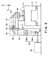
- Figure 3 is a schematic view of an illumination optical system which can be incorporated into the exposure apparatus of Figures 1 and 2.
- Figure 4 is a flow chart of the procedure for manufacture of microdevices, by use of the exposure apparatus of Figure 1.
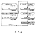
- Figure 5 is a flow chart for explaining details of a wafer process, included in the procedure of Figure 4.
- FIG 1 is a schematic view of an exposure apparatus according to an embodiment of the present invention, as seen from the side.
- Figure 2 is a perspective view of this exposure apparatus.
- the exposure apparatus comprises a step-and-scan type exposure apparatus wherein a portion of a pattern of a reticle is projected by a projection optical system 2 on to a wafer placed on a fine-motion stage mechanism 80, mounted on an X-Y stage mechanism 3, wherein the reticle and the wafer are relatively and scanningly moved in synchronism with each other in Y direction relative to the projection optical system 2, whereby the pattern of the reticle is transferred to the wafer, and wherein there is stepwise motion interposed to repeat the scan exposure to plural regions on the wafer.
- Motion of the reticle in scan direction is provided by a reticle side stage mechanism having a linear motor 4 wherein a thrust is produced between a stator 4a and a movable element 4b by which the movable element 4b can be moved in the scan direction.
- the reticle stage 1 is connected to this movable element 4b.
- the stator 4a is supported by first supporting means 101, with a freedom in Y direction. Also, it is supported by second supporting means 105, rigidly in Y direction and flexibly in other directions.
- the second supporting means 105 includes a pillar 103 extending upwardly from a base frame 10, and one-axis supporting means 102 extending in Y direction from the pillar 103 and for supporting the stator 4a rigidly in Y direction and flexibly in other directions.
- the reticle stage 1 can be moved in Y direction by the linear motor 4.
- the X-Y stage mechanism 3 comprises an X stage 3a which can be moved in X direction by a linear motor 5.
- the wafer stage further comprises a Y stage 3b which can be moved in Y direction by a linear motor 6. Synchronized scan of the reticle and the wafer is provided by moving the reticle stage 1 and the Y stage 3b in Y direction at a predetermined speed ratio (e.g., 4:1). Stepwise motion in X direction is provided by the X stage 3a.
- the X-Y stage 3 is mounted on a stage base 7 which is supported by the floor, for example, at three points and through three dampers 8.
- the first supporting means 101 and the projection optical system 2 are mounted on a barrel base 9 which is supported by the base frame 10 through three dampers 11 and pillars 12.
- Each damper 8 comprises an active damper for active vibration control or vibration isolation in six-axis direction. However, it may comprise a passive damper. Alternatively, the mechanism may be supported without such damper.
- a wafer is conveyed along a conveyance path between two pillars 12 in the front portion of the apparatus, on to the X-Y stage 3.
- the exposure apparatus performs printing of the pattern of the reticle on to plural exposure regions on the wafer while repeating scan exposure and stepwise motion.
- the reticle stage 1 and the Y stage 3b are moved in Y direction (scan direction) at a predetermined speed ratio so that the pattern of the reticle is scanned with slit-like exposure light, and also the wafer is scanned with the projected image thereof.
- the pattern of the reticle is transferred and printed on to a particular exposure region on the wafer.
- the X stage 3a is driven in X direction to move the wafer stepwise to thereby place another exposure region at the scan exposure start position. Then, the scan exposure is performed.
- the layout of exposure regions, the scan direction (positive or negative) and the order of exposures for the exposure regions, for example, are so determined that, with the combination of stepwise motion in X direction and movement in Y direction for scan exposure, the exposures can be done efficiently to plural exposure regions on the wafer.
- FIG 3 is a schematic view of the structure of an illumination optical system which can be incorporated into the exposure apparatus of Figures 1 and 2.
- the projection optical system (not shown) and the reticle stage 1 are mounted on a barrel base (main structure) 9 which is supported by dampers.
- the illumination optical system is divided into a main portion (first portion) 31 fixedly supported by the barrel base 9 through a support table 41, and a floor-supported portion (second portion) 32 directly disposed on the floor.
- the direction of displacement of the barrel base 9 which depends on the position of the reticle stage 1 during the scan is included in a plane which contains the optical axis direction, at the portion 33 where the illumination optical system is divided, and a direction corresponding to the scan direction (Y direction).
- the direction corresponding to the scan direction means a direction in which, when the optical axis of the illumination light shifts on the reticle in the scan direction, the optical axis at the division portion 33 shifts. In this example, it is Z direction.
- the direction of displacement of the barrel base 9 lies on Y-Z plane.
- the floor-supported portion 32 includes a mirror 35 for reflecting, upwardly, a beam of pulsed light as emitted horizontally from an excimer laser (light source) 34, a beam shaping optical system 36 for adjusting the shape of the beam from the mirror 35, incoherency transformation means 37 for transforming the shaped beam into coherent light, by dividing and deflecting it with time, for example, and a mirror 38 for reflecting the light from the incoherency transformation means 37 toward the main portion 31 (in Y direction).
- the beam shaping optical system 36 comprises a concave lens 36a for diverging the beam from the mirror 35, and a convex lens 36b for transforming the divergent beam from the concave lens 36a into parallel light.
- the main portion 31 comprises a fly's eye lens 39 for receiving the light from the mirror 38 of the floor-supported portion 32 and for forming secondary light sources, a mirror 40 for reflecting downwardly (Z direction) the light emitted in Y direction from the fly's eye lens 39, and a condensing lens 42 for collecting the light from the mirror 40 and for illuminating a predetermined range of the reticle which is placed on the reticle stage 1. While not shown in the drawing, the main portion 31 further includes a masking blade for shaping the illumination light into a slit-like shape in X direction.
- the barrel base 9 displaces along the Y-Z plane due to shift of the gravity center thereof.
- the relative position between the main portion 31 and the floor-supported portion 32 of the illumination optical system changes.
- Such relative displacement occurs in Y-Z plane, but the displacement in Y direction corresponds, in the sense of optics, to a change in distance between the mirror 38 and the fly's eye lens 39. It does not cause a change in symmetry of the beam entering the fly's eye lens 39. Therefore, with the displacement component in Y direction, there occurs no change in illuminance distribution, within the illumination region upon the reticle.
- displacement in Z direction causes a change in position of the beam entering the fly's eye lens 39, in Z direction.
- it produces non-uniform illuminance which is asymmetric with respect to Y direction, i.e., to the scan direction. Since however, in scan exposure, there occurs no dispersion of exposure amount unless, in the illumination region, the distribution of light quantity as integrated in the scan direction changes. Thus, with the displacement component in Z direction, the distribution of exposure amount does not become non-uniform.
- the motion of the reticle stage 1 in the scan direction provides scan exposure with uniform exposure amount distribution.
- the fly's eye lens 39 is fixedly supported by the main portion which is fixedly held by the barrel base 9, the relative position of the optical axis of the illumination light after the fly's eye lens 39 with respect to the barrel base 9 is kept constant, continuously. Therefore, regardless of any tilt of the barrel base 9, the position of the illumination region upon the reticle is held constant, continuously.
- FIG 4 is a flow chart of procedure for manufacture of microdevices such as semiconductor chips (e.g. ICs or LSIs), liquid crystal panels, CCDs, thin film magnetic heads or micro-machines, for example.
- Step 31 is a design process for designing a circuit of a semiconductor device.
- Step 32 is a process for making a mask on the basis of the circuit pattern design.
- Step 33 is a process for preparing a wafer by using a material such as silicon.
- Step 34 is a wafer process which is called a pre-process wherein, by using the so prepared mask and wafer, circuits are practically formed on the wafer through lithography.
- Step 35 subsequent to this is an assembling step which is called a post-process wherein the wafer having been processed by step 34 is formed into semiconductor chips.
- This step includes assembling (dicing and bonding) process and packaging (chip sealing) process.
- Step 36 is an inspection step wherein operation check, durability check and so on for the semiconductor devices provided by step 35, are carried out. With these processes, semiconductor devices are completed and they are shipped (step 37).
- Step 41 is an oxidation process for oxidizing the surface of a wafer.
- Step 42 is a CVD process for forming an insulating film on the wafer surface.
- Step 43 is an electrode forming process for forming electrodes upon the wafer by vapor deposition.
- Step 44 is an ion implanting process for implanting ions to the wafer.
- Step 45 is a resist process for applying a resist (photosensitive material) to the wafer.
- Step 46 is an exposure process for printing, by exposure, the circuit pattern of the mask on the wafer through the exposure apparatus described above.
- Step 47 is a developing process for developing the exposed wafer.
- Step 48 is an etching process for removing portions other than the developed resist image.
- Step 49 is a resist separation process for separating the resist material remaining on the wafer after being subjected to the etching process. By repeating these processes, circuit patterns are superposedly formed on the wafer.
- the illumination optical system is divided into a main portion being disposed on a main structure and a floor-supported portion being directly disposed on a floor. This assures that the direction of displacement of the main structure which depends on the position of a mask stage during the scan is laid within a plane which includes the optical axis direction, at the location where the illumination optical system is divided, and a direction corresponding to the scan direction. As a result, scan exposure with uniform exposure amount distribution is enabled.
- a secondary light source forming means for providing light as a secondary light source is disposed on the main portion of the illumination optical system, the position of the illumination region on the reticle can be held constant, continuously. This enables scan exposure with more uniform exposure amount distribution.
Landscapes
- Physics & Mathematics (AREA)
- General Physics & Mathematics (AREA)
- Health & Medical Sciences (AREA)
- Engineering & Computer Science (AREA)
- Environmental & Geological Engineering (AREA)
- Epidemiology (AREA)
- Public Health (AREA)
- Exposure And Positioning Against Photoresist Photosensitive Materials (AREA)
- Exposure Of Semiconductors, Excluding Electron Or Ion Beam Exposure (AREA)
Applications Claiming Priority (3)
| Application Number | Priority Date | Filing Date | Title |
|---|---|---|---|
| JP27985496A JP3283767B2 (ja) | 1996-10-02 | 1996-10-02 | 露光装置およびデバイス製造方法 |
| JP279854/96 | 1996-10-02 | ||
| JP27985496 | 1996-10-02 |
Publications (3)
| Publication Number | Publication Date |
|---|---|
| EP0834772A2 true EP0834772A2 (fr) | 1998-04-08 |
| EP0834772A3 EP0834772A3 (fr) | 1998-12-23 |
| EP0834772B1 EP0834772B1 (fr) | 2004-01-02 |
Family
ID=17616876
Family Applications (1)
| Application Number | Title | Priority Date | Filing Date |
|---|---|---|---|
| EP97307732A Expired - Lifetime EP0834772B1 (fr) | 1996-10-02 | 1997-10-01 | Appareil d'exposition |
Country Status (6)
| Country | Link |
|---|---|
| US (1) | US6008885A (fr) |
| EP (1) | EP0834772B1 (fr) |
| JP (1) | JP3283767B2 (fr) |
| KR (1) | KR100276796B1 (fr) |
| DE (1) | DE69727016T2 (fr) |
| TW (1) | TW420842B (fr) |
Cited By (3)
| Publication number | Priority date | Publication date | Assignee | Title |
|---|---|---|---|---|
| JP2004207711A (ja) * | 2002-12-10 | 2004-07-22 | Nikon Corp | 露光装置及び露光方法、デバイス製造方法 |
| US6891603B2 (en) | 2000-12-28 | 2005-05-10 | Nikon Corporation | Manufacturing method in manufacturing line, manufacturing method for exposure apparatus, and exposure apparatus |
| JP2009105471A (ja) * | 2002-12-10 | 2009-05-14 | Nikon Corp | 露光装置、及びデバイス製造方法 |
Families Citing this family (15)
| Publication number | Priority date | Publication date | Assignee | Title |
|---|---|---|---|---|
| AU1260099A (en) * | 1997-11-25 | 1999-06-15 | Nikon Corporation | Projection exposure system |
| KR100574208B1 (ko) | 1998-06-02 | 2006-04-27 | 가부시키가이샤 니콘 | 주사형 노광장치 및 그의 제조방법, 및 디바이스 제조방법 |
| CN1309017C (zh) * | 1998-11-18 | 2007-04-04 | 株式会社尼康 | 曝光方法和装置 |
| US6727981B2 (en) | 1999-07-19 | 2004-04-27 | Nikon Corporation | Illuminating optical apparatus and making method thereof, exposure apparatus and making method thereof, and device manufacturing method |
| JP2001148341A (ja) * | 1999-11-19 | 2001-05-29 | Nikon Corp | 露光装置 |
| TW538256B (en) * | 2000-01-14 | 2003-06-21 | Zeiss Stiftung | Microlithographic reduction projection catadioptric objective |
| WO2002044786A2 (fr) * | 2000-11-28 | 2002-06-06 | Carl Zeiss Smt Ag | Systeme de projection catadioptrique pour une lithographie a 157 nm |
| JP3728180B2 (ja) | 2000-06-01 | 2005-12-21 | キヤノン株式会社 | 干渉計搭載ステージ |
| US6774981B1 (en) * | 2000-09-08 | 2004-08-10 | Nikon Corporation | Modular exposure apparatus with removable optical device and improved isolation of the optical device |
| JP3495992B2 (ja) * | 2001-01-26 | 2004-02-09 | キヤノン株式会社 | 補正装置、露光装置、デバイス製造方法及びデバイス |
| WO2002103766A1 (fr) * | 2001-06-13 | 2002-12-27 | Nikon Corporation | Procede et systeme d'exposition au balayage, et procede de production d'un dispositif associe |
| US8208198B2 (en) | 2004-01-14 | 2012-06-26 | Carl Zeiss Smt Gmbh | Catadioptric projection objective |
| US20080151364A1 (en) | 2004-01-14 | 2008-06-26 | Carl Zeiss Smt Ag | Catadioptric projection objective |
| KR101376931B1 (ko) | 2004-05-17 | 2014-03-25 | 칼 짜이스 에스엠티 게엠베하 | 중간이미지를 갖는 카타디옵트릭 투사 대물렌즈 |
| KR102015401B1 (ko) * | 2012-12-21 | 2019-08-29 | 삼성디스플레이 주식회사 | 광학계 및 기판 밀봉 방법 |
Family Cites Families (16)
| Publication number | Priority date | Publication date | Assignee | Title |
|---|---|---|---|---|
| JPS5999722A (ja) * | 1982-11-29 | 1984-06-08 | Canon Inc | 半導体焼付露光制御方法 |
| WO1986000427A1 (fr) * | 1984-06-21 | 1986-01-16 | American Telephone & Telegraph Company | Lithographie a rayons ultraviolets profonds |
| US4724466A (en) * | 1986-01-17 | 1988-02-09 | Matsushita Electric Industrial Co., Ltd. | Exposure apparatus |
| JP2728898B2 (ja) * | 1988-10-05 | 1998-03-18 | キヤノン株式会社 | 露光装置 |
| US5204711A (en) * | 1990-06-08 | 1993-04-20 | Nippon Seiko Kabushiki Kaisha | Projection exposure device |
| JP3182158B2 (ja) * | 1991-02-25 | 2001-07-03 | キヤノン株式会社 | 露光装置用のステージ支持装置 |
| JP2830492B2 (ja) * | 1991-03-06 | 1998-12-02 | 株式会社ニコン | 投影露光装置及び投影露光方法 |
| US5281996A (en) * | 1992-09-04 | 1994-01-25 | General Signal Corporation | Photolithographic reduction imaging of extended field |
| JPH06302491A (ja) * | 1993-04-15 | 1994-10-28 | Nikon Corp | 露光量制御装置 |
| JP3255312B2 (ja) * | 1993-04-28 | 2002-02-12 | 株式会社ニコン | 投影露光装置 |
| JPH07211620A (ja) * | 1994-01-25 | 1995-08-11 | Sony Corp | 半導体露光装置 |
| JP3506158B2 (ja) * | 1995-04-14 | 2004-03-15 | 株式会社ニコン | 露光装置及び走査型露光装置、並びに走査露光方法 |
| US5508518A (en) * | 1995-05-03 | 1996-04-16 | International Business Machines Corporation | Lithography tool with vibration isolation |
| KR960042227A (ko) * | 1995-05-19 | 1996-12-21 | 오노 시게오 | 투영노광장치 |
| US5721606A (en) * | 1995-09-07 | 1998-02-24 | Jain; Kanti | Large-area, high-throughput, high-resolution, scan-and-repeat, projection patterning system employing sub-full mask |
| US5798838A (en) * | 1996-02-28 | 1998-08-25 | Nikon Corporation | Projection exposure apparatus having function of detecting intensity distribution of spatial image, and method of detecting the same |
-
1996
- 1996-10-02 JP JP27985496A patent/JP3283767B2/ja not_active Expired - Fee Related
-
1997
- 1997-09-29 US US08/941,629 patent/US6008885A/en not_active Expired - Lifetime
- 1997-10-01 EP EP97307732A patent/EP0834772B1/fr not_active Expired - Lifetime
- 1997-10-01 TW TW086114308A patent/TW420842B/zh not_active IP Right Cessation
- 1997-10-01 DE DE69727016T patent/DE69727016T2/de not_active Expired - Lifetime
- 1997-10-01 KR KR1019970050764A patent/KR100276796B1/ko not_active Expired - Fee Related
Cited By (3)
| Publication number | Priority date | Publication date | Assignee | Title |
|---|---|---|---|---|
| US6891603B2 (en) | 2000-12-28 | 2005-05-10 | Nikon Corporation | Manufacturing method in manufacturing line, manufacturing method for exposure apparatus, and exposure apparatus |
| JP2004207711A (ja) * | 2002-12-10 | 2004-07-22 | Nikon Corp | 露光装置及び露光方法、デバイス製造方法 |
| JP2009105471A (ja) * | 2002-12-10 | 2009-05-14 | Nikon Corp | 露光装置、及びデバイス製造方法 |
Also Published As
| Publication number | Publication date |
|---|---|
| EP0834772A3 (fr) | 1998-12-23 |
| DE69727016T2 (de) | 2004-11-25 |
| KR100276796B1 (ko) | 2001-01-15 |
| JPH10106940A (ja) | 1998-04-24 |
| US6008885A (en) | 1999-12-28 |
| EP0834772B1 (fr) | 2004-01-02 |
| JP3283767B2 (ja) | 2002-05-20 |
| TW420842B (en) | 2001-02-01 |
| DE69727016D1 (de) | 2004-02-05 |
| KR19980032469A (ko) | 1998-07-25 |
Similar Documents
| Publication | Publication Date | Title |
|---|---|---|
| US6008885A (en) | Scanning exposure apparatus | |
| US5933215A (en) | Exposure apparatus and device manufacturing method using the same | |
| US5917580A (en) | Scan exposure method and apparatus | |
| JP2001358062A (ja) | 露光方法及び露光装置 | |
| EP0753796A1 (fr) | Appareil d'exposition par balayage et méthode de fabrication d'un dispositif utilisant celui-ci | |
| JPH1041225A (ja) | 照明装置及びそれを用いた投影露光装置 | |
| US6641981B1 (en) | Exposure method, exposure apparatus, and device manufacturing method | |
| KR100614295B1 (ko) | 디바이스 제조방법, 그 디바이스 및 그를 위한 리소그래피장치 | |
| EP0833209B1 (fr) | Appareil d'exposition par balayage et méthode de fabrication d'un dispositif l'utilisant | |
| US6069683A (en) | Scanning exposure method and apparatus | |
| US5907390A (en) | Positioning apparatus, exposure apparatus and method of manufacturing semiconductor device | |
| US8736813B2 (en) | Exposure apparatus with an illumination system generating multiple illumination beams | |
| US20010006422A1 (en) | Stage system in projection exposure apparatus | |
| JP2006120798A (ja) | 露光装置 | |
| EP1037114A2 (fr) | Méthode de commande d' un porte-objet, appareil d' exposition et méthode de fabrication d' un dispositif | |
| JPH1092727A (ja) | 投影露光装置 | |
| JPH09223662A (ja) | 照明装置、走査型露光装置及びそれらを用いたデバイスの製造方法 | |
| US11067900B2 (en) | Dense line extreme ultraviolet lithography system with distortion matching | |
| US6307616B1 (en) | Exposure apparatus and substrate handling system therefor | |
| JP2004158689A (ja) | 走査型露光方法及び走査型露光装置 | |
| JP2004172470A (ja) | ブラインド駆動方法と照明領域規制装置および走査型露光方法並びに走査型露光装置 | |
| JPH11329954A (ja) | 走査型露光装置およびデバイス製造方法 | |
| JP2000049074A (ja) | ステージ制御方法、ステージ装置および露光装置 | |
| JP2000173910A (ja) | 投影露光装置 | |
| JPH1032164A (ja) | 走査型露光装置及びそれを用いたデバイスの製造方法 |
Legal Events
| Date | Code | Title | Description |
|---|---|---|---|
| PUAI | Public reference made under article 153(3) epc to a published international application that has entered the european phase |
Free format text: ORIGINAL CODE: 0009012 |
|
| AK | Designated contracting states |
Kind code of ref document: A2 Designated state(s): DE GB NL |
|
| PUAL | Search report despatched |
Free format text: ORIGINAL CODE: 0009013 |
|
| AK | Designated contracting states |
Kind code of ref document: A3 Designated state(s): AT BE CH DE DK ES FI FR GB GR IE IT LI LU MC NL PT SE |
|
| 17P | Request for examination filed |
Effective date: 19990506 |
|
| AKX | Designation fees paid |
Free format text: DE GB NL |
|
| 17Q | First examination report despatched |
Effective date: 19991214 |
|
| GRAG | Despatch of communication of intention to grant |
Free format text: ORIGINAL CODE: EPIDOS AGRA |
|
| GRAG | Despatch of communication of intention to grant |
Free format text: ORIGINAL CODE: EPIDOS AGRA |
|
| GRAG | Despatch of communication of intention to grant |
Free format text: ORIGINAL CODE: EPIDOS AGRA |
|
| GRAH | Despatch of communication of intention to grant a patent |
Free format text: ORIGINAL CODE: EPIDOS IGRA |
|
| GRAS | Grant fee paid |
Free format text: ORIGINAL CODE: EPIDOSNIGR3 |
|
| GRAA | (expected) grant |
Free format text: ORIGINAL CODE: 0009210 |
|
| AK | Designated contracting states |
Kind code of ref document: B1 Designated state(s): DE GB NL |
|
| REG | Reference to a national code |
Ref country code: GB Ref legal event code: FG4D |
|
| REF | Corresponds to: |
Ref document number: 69727016 Country of ref document: DE Date of ref document: 20040205 Kind code of ref document: P |
|
| PLBE | No opposition filed within time limit |
Free format text: ORIGINAL CODE: 0009261 |
|
| 26N | No opposition filed |
Effective date: 20041005 |
|
| PGFP | Annual fee paid to national office [announced via postgrant information from national office to epo] |
Ref country code: GB Payment date: 20091028 Year of fee payment: 13 |
|
| GBPC | Gb: european patent ceased through non-payment of renewal fee |
Effective date: 20101001 |
|
| PG25 | Lapsed in a contracting state [announced via postgrant information from national office to epo] |
Ref country code: GB Free format text: LAPSE BECAUSE OF NON-PAYMENT OF DUE FEES Effective date: 20101001 |
|
| PGFP | Annual fee paid to national office [announced via postgrant information from national office to epo] |
Ref country code: DE Payment date: 20151031 Year of fee payment: 19 |
|
| PGFP | Annual fee paid to national office [announced via postgrant information from national office to epo] |
Ref country code: NL Payment date: 20150908 Year of fee payment: 19 |
|
| REG | Reference to a national code |
Ref country code: DE Ref legal event code: R119 Ref document number: 69727016 Country of ref document: DE |
|
| REG | Reference to a national code |
Ref country code: NL Ref legal event code: MM Effective date: 20161101 |
|
| PG25 | Lapsed in a contracting state [announced via postgrant information from national office to epo] |
Ref country code: DE Free format text: LAPSE BECAUSE OF NON-PAYMENT OF DUE FEES Effective date: 20170503 |
|
| PG25 | Lapsed in a contracting state [announced via postgrant information from national office to epo] |
Ref country code: NL Free format text: LAPSE BECAUSE OF NON-PAYMENT OF DUE FEES Effective date: 20161101 |