EP0838853A2 - Circuit intégré et sa fabrication - Google Patents
Circuit intégré et sa fabrication Download PDFInfo
- Publication number
- EP0838853A2 EP0838853A2 EP97307999A EP97307999A EP0838853A2 EP 0838853 A2 EP0838853 A2 EP 0838853A2 EP 97307999 A EP97307999 A EP 97307999A EP 97307999 A EP97307999 A EP 97307999A EP 0838853 A2 EP0838853 A2 EP 0838853A2
- Authority
- EP
- European Patent Office
- Prior art keywords
- integrated circuit
- composition
- substrate
- hydrocarbyl group
- alkyl
- Prior art date
- Legal status (The legal status is an assumption and is not a legal conclusion. Google has not performed a legal analysis and makes no representation as to the accuracy of the status listed.)
- Withdrawn
Links
- 0 C1C2NCC2*1 Chemical compound C1C2NCC2*1 0.000 description 1
Images

Classifications
-
- H—ELECTRICITY
- H10—SEMICONDUCTOR DEVICES; ELECTRIC SOLID-STATE DEVICES NOT OTHERWISE PROVIDED FOR
- H10W—GENERIC PACKAGES, INTERCONNECTIONS, CONNECTORS OR OTHER CONSTRUCTIONAL DETAILS OF DEVICES COVERED BY CLASS H10
- H10W70/00—Package substrates; Interposers; Redistribution layers [RDL]
- H10W70/60—Insulating or insulated package substrates; Interposers; Redistribution layers
- H10W70/67—Insulating or insulated package substrates; Interposers; Redistribution layers characterised by their insulating layers or insulating parts
- H10W70/69—Insulating materials thereof
-
- Y—GENERAL TAGGING OF NEW TECHNOLOGICAL DEVELOPMENTS; GENERAL TAGGING OF CROSS-SECTIONAL TECHNOLOGIES SPANNING OVER SEVERAL SECTIONS OF THE IPC; TECHNICAL SUBJECTS COVERED BY FORMER USPC CROSS-REFERENCE ART COLLECTIONS [XRACs] AND DIGESTS
- Y10—TECHNICAL SUBJECTS COVERED BY FORMER USPC
- Y10S—TECHNICAL SUBJECTS COVERED BY FORMER USPC CROSS-REFERENCE ART COLLECTIONS [XRACs] AND DIGESTS
- Y10S428/00—Stock material or miscellaneous articles
- Y10S428/901—Printed circuit
-
- Y—GENERAL TAGGING OF NEW TECHNOLOGICAL DEVELOPMENTS; GENERAL TAGGING OF CROSS-SECTIONAL TECHNOLOGIES SPANNING OVER SEVERAL SECTIONS OF THE IPC; TECHNICAL SUBJECTS COVERED BY FORMER USPC CROSS-REFERENCE ART COLLECTIONS [XRACs] AND DIGESTS
- Y10—TECHNICAL SUBJECTS COVERED BY FORMER USPC
- Y10T—TECHNICAL SUBJECTS COVERED BY FORMER US CLASSIFICATION
- Y10T428/00—Stock material or miscellaneous articles
- Y10T428/24—Structurally defined web or sheet [e.g., overall dimension, etc.]
- Y10T428/24802—Discontinuous or differential coating, impregnation or bond [e.g., artwork, printing, retouched photograph, etc.]
- Y10T428/24917—Discontinuous or differential coating, impregnation or bond [e.g., artwork, printing, retouched photograph, etc.] including metal layer
-
- Y—GENERAL TAGGING OF NEW TECHNOLOGICAL DEVELOPMENTS; GENERAL TAGGING OF CROSS-SECTIONAL TECHNOLOGIES SPANNING OVER SEVERAL SECTIONS OF THE IPC; TECHNICAL SUBJECTS COVERED BY FORMER USPC CROSS-REFERENCE ART COLLECTIONS [XRACs] AND DIGESTS
- Y10—TECHNICAL SUBJECTS COVERED BY FORMER USPC
- Y10T—TECHNICAL SUBJECTS COVERED BY FORMER US CLASSIFICATION
- Y10T428/00—Stock material or miscellaneous articles
- Y10T428/31504—Composite [nonstructural laminate]
- Y10T428/31678—Of metal
- Y10T428/31681—Next to polyester, polyamide or polyimide [e.g., alkyd, glue, or nylon, etc.]
-
- Y—GENERAL TAGGING OF NEW TECHNOLOGICAL DEVELOPMENTS; GENERAL TAGGING OF CROSS-SECTIONAL TECHNOLOGIES SPANNING OVER SEVERAL SECTIONS OF THE IPC; TECHNICAL SUBJECTS COVERED BY FORMER USPC CROSS-REFERENCE ART COLLECTIONS [XRACs] AND DIGESTS
- Y10—TECHNICAL SUBJECTS COVERED BY FORMER USPC
- Y10T—TECHNICAL SUBJECTS COVERED BY FORMER US CLASSIFICATION
- Y10T428/00—Stock material or miscellaneous articles
- Y10T428/31504—Composite [nonstructural laminate]
- Y10T428/31721—Of polyimide
Definitions
- the present invention relates to an integrated circuit comprising an improved dielectric material and process for manufacturing the integrated circuit.
- the present dielectric is silicon dioxide which has a dielectric constant of about 4.0. This material has the requisite mechanical and thermal properties to withstand processing operations and thermal cycling associated with semiconductor manufacturing. However, it is desired that dielectric materials for future integrated circuit devices exhibit a lower dielectric constant (e.g., ⁇ 3.0) than exhibited by silicon dioxide.
- the present invention relates to an integrated circuit device comprising (i) a substrate; (ii) interconnecting metallic circuit lines positioned on the substrate and (iii) a dielectric material positioned contiguous to the circuit lines (over and/or between the circuit lines).
- the dielectric material comprises the reaction product of an organic polysilica and polyamic ester terminated preferably with a trialkoxysilylalkyl group.
- the organic polysilica is silsesquioxane and the dielectric material has phase domains less than 0.5 microns.
- the organic polysilica is C 1-6 alkoxysilane, silsesquioxane or mixture thereof, in particular wherein the polyamic ester is terminated with a tri C 1-10 alkoxysilyl C 1-10 alkyl group or tri C 1-10 alkoxysilylaryl group.
- the dielectric composition preferably has a dielectric constant of less than 3.2.
- the silsesquioxane is phenyl/C 1-6 alkyl silsesquioxane, in particular wherein the polyamic ester comprises a diamine selected from 9,9'-bis (4-aminophenyl) fluorene; 4,4' oxydianiline and 1,1-bis (4-aminophenyl)-1-phenyl-2,2,2-trifluoroethane and a diester diacid halide selected from di C 1-6 alkyl dichloro pyromellitate; di C 1-6 alkyl dichloroxydiphthalate and di C 1-6 alkyl dichlorobiphenyl-tetracarboxylate.
- the polyamic ester comprises a diamine selected from 9,9'-bis (4-aminophenyl) fluorene; 4,4' oxydianiline and 1,1-bis (4-aminophenyl)-1-phenyl-2,2,2-trifluoroethane and a diester diacid halide selected
- the integrated circuit device will be such that the dielectric composition has phase domains less than 0.5 microns.
- a process for forming an integrated circuit comprising: (a) positioning on a substrate a layer of dielectric composition, the composition comprising reactants organic polysilica and polyamic ester terminated with (RO) m (R") n SiR'- where R and R' are independently a hydrocarbyl group; R" is hydrid
- the organic polysilica is C 1-6 alkoxysilane, silsesquioxane or mixtures thereof, in particular the polyamic ester is terminated with tri C 1-10 alkoxysilyl C 1-10 alkyl group or a tri C 1-10 alkoxysilyl aryl group.
- the polyamic ester comprises a diamine selected from 9,9'-bis (4-aminophenyl) fluorene; 4,4'oxydianiline and 1,1-bis (4-aminophenyl) - 1-phenyl-2,2,2-trifluoroethane and a diester diacid halide selected from di C 1-6 alkyl dichloro pyromellitate; di C 1-6 alkyl dichloroxydiphthalate and di C 1-6 alkyl dichlorobiphenyl-tetracarboxylate.
- the composition is heated in the presence of an organic base.
- the organic polysilica is C 1-6 alkoxysilane, silsesquioxane or mixtures thereof, in particular the polyamic ester is end capped with a tri C 1-10 alkoxysilyl C 1-10 alkyl group or a tri C 10 alkoxysilylaryl group.
- the polyamic ester comprises a diamine selected from 9,9'-bis (4-aminophenyl) fluorene; 4,4'oxydianiline and 1,1-bis (4-aminophenyl)-1-phenyl-2,2,2-trifluoroethane and a diester diacid halide selected from di C 1-6 alkyl dichloro pyromellitate; di C 1-6 alkyl dichlorooxydiphthalate and di C 1-6 alkyl dichlorobiphenyl-tetra carboxylate.
- a diamine selected from 9,9'-bis (4-aminophenyl) fluorene; 4,4'oxydianiline and 1,1-bis (4-aminophenyl)-1-phenyl-2,2,2-trifluoroethane
- a diester diacid halide selected from di C 1-6 alkyl dichloro pyromellitate; di C 1-6 alkyl dichlorooxydiphthalate and di C 1-6 alkyl dichlor
- the composition is heated in the presence of an organic base.
- the organic polysilica is C 1-6 alkoxysilane, silsesquioxane or mixtures thereof, in particular the polyamic ester is end capped with a tri C 1-10 alkoxysilyl C 1-10 alkyl group or a tri C 1-10 alkoxysilylaryl group.
- the polyamic ester comprises a diamine selected from 9,9'-bis(4-aminophenyl) fluorene; 4,4'oxydianiline and 1,1-bis(4-aminophenyl)-1-phenyl,2,2,2trifluoroethane and a diester diacid halide selected from di C 1-6 alkyl dichloro pyromellitate; di C 1-6 alkyl dichlorooxydiphthalate and di C 1-6 alkyl dichorobiphenyl-tetra carboxylate.
- the organic polysilica is C 1-6 alkoxysilane, silsesquioxane or mixture thereof, in particular the silsesquioxane is phenyl/C 1-6 alkyl silsesquioxane.
- the polyamic ester is terminated with a tri-C 1-10 alkoxysilyl C 1-10 alkyl group or tri C 1-10 alkoxysilylaryl group, and in particular the polyamic ester comprises a diamine selected from 9,9'bis(4-aminophenyl) fluorene, 4,4' oxydianiline and 1,1-bis (4aminophenyl)-1-phenyl-2,2,2-trifluoroethane, and a diester diacid halide selected from di C 1-6 alkyl dichloro pyromellitate, di C 1-6 alkyl dichlorooxydiphthalate and di C 1-6 alkyl dichlorobiphenyl-tetracarboxylate.
- a diamine selected from 9,9'bis(4-aminophenyl) fluorene, 4,4' oxydianiline and 1,1-bis (4aminophenyl)-1-phenyl-2,2,2-trifluoroethane
- the present invention also relates to an integrated circuit packaging structure, the material composition and the processes for forming the integrated circuit device of the present invention.
- the device generally comprises substrate 2, metallic circuit lines 4 and dielectric material 6.
- the substrate 2 has vertical metallic studs 8 formed therein.
- the circuit lines function to distribute electrical signals in the device and to provide power input to and signal output from the device.
- Suitable integrated circuit devices will generally comprise multiple layers of circuit lines which are interconnected by vertical metallic studs.
- Suitable substrates for the device of the present invention comprises silicon, silicon dioxide, glass, silicon nitride, ceramics, aluminum, copper and gallium arsenide. Other suitable substrates will be known to those skilled in the art.
- an underlying layer of insulated, planarized circuit lines can also function as a substrate.
- Suitable circuit lines generally comprise a metallic, electrically conductive material such as copper, aluminum, tungsten, gold, silver or alloys thereof.
- the circuit lines may be coated with a metallic liner such as a layer of nickel, tantalum or chromium or other layers such as barrier or adhesion layers (e.g., SiN, TiN).
- an integrated circuit packaging device for providing signal and power current to a one or more integrated circuit chips
- a substrate having electrical conductor for connection to a circuit board, (ii) a plurality of alternating electrically insulating and conducting layers positioned on the substrate wherein at least of the conducting layers comprises the improved dielectric film of the present invention and (iii) a plurality of vias for electrically interconnecting electrical conductor, conducting layers and integrated circuit chips.
- the integrated circuit packaging device is an intermediate level of packaging between the integrated circuit chip and the circuit board.
- the integrated circuit chips are mounted on the integrated circuit packaging device which is in turn mounted on the circuit board.
- the substrate of the packaging device is generally an inert substrate such as glass, silicon or ceramic.
- the substrate can optionally have integrated circuits disposed therein.
- the substrate is provided with electrical conductor such as input/output pins (I/O pins) for electrically connecting the packaging device to the circuit board.
- I/O pins input/output pins
- a plurality of electrically insulating and electrically conducting layers are alternatively stacked up on the substrate. The layers are generally formed on the substrate in a layer by layer process wherein each layer is formed in a separate process step.
- the packaging device also comprises receiving means for receiving the integrated circuit chips. Suitable receiving means include pinboards for receipt of chip I/O pins or metal pads for solder connection to the chip. Generally, the packaging device also comprises a plurality of electrical vias generally vertically aligned to electrically interconnect the I/O pins, the conductive layers and integrated circuit chips disposed in the receiving means.
- the function structure and method of manufacture of the integrated circuit packaging devices are well known to those skilled in the art disclosed in U.S. Patent Nos. 4,489,364, 4,508,981, 4,628,411 and 4,811,082, the disclosures of which are incorporated herein by reference.
- the key feature of the present invention is the dielectric material which is positioned over the circuit lines and/or between the circuit lines and on the substrate.
- the dielectric material is often planarized to function as a substrate for lithographic formation of the next layer of circuit lines.
- the end group is preferably a mono, di or tri C 1-6 alkoxysilyl C 1-6 alkyl or aryl group (e.g., phenylene, benzylene, napthylene or anthracenylene) group.
- hydrocarbyl group means hydrocarbon based group (mono or difunctional) having a carbon atom attached to the remainder of the molecule and having predominantly hydrocarbon character. Hydrocarbyl groups include the following:
- the polyamic ester with the end group is preferably formed from the reaction of (i) a diamine; (ii) a diester diacyl halide (preferably chloride) and (iii) an aminoalkoxysilane.
- Suitable diamines have the formula H 2 NRNH 2 wherein R is wherein X is selected from the group consisting of an alkylene chain having 1-3 carbon or halocarbon atoms, carbonyl, -O-, -S-, -SO 2 - and -N- alkyl.
- the alkylene chain can further be substituted with haloalkyl (e.g., trifluoro-methyl) and phenyl.
- the aromatic ring can optionally be substituted by a e.g., trifluoromethoxy or the like.
- Suitable R for the diamine include: where y is selected from trifluoromethyl, phenyl or substituted phenyl.
- Suitable aromatic diamines are:
- the R in the diamine may also be an aliphatic or cycloaliphatic group such as cycloalkylene e.g., cyclohexylene.
- Suitable aliphatic diamines include 1,4-diaminocyclohexane and bis (4-aminocyclohexyl) methane.
- a preferred diamine is a diamine wherein x in the above formula is >C (phenyl) (trifluoromethyl) .
- Preferred diamines are 9,9'-bis (4aminophenyl) fluorene (FDA); 4,4'-oxydianiline and 1,1-bis (4aminophenyl)-1-phenyl-2,2,2-trifluoroethane (3FDA).
- the diester diacyl chloride is suitably made from the corresponding dianhydride suitably having the formula wherein Ar may be selected from.
- Suitable dianhydrides include:
- a preferred diester diacyl chloride is diethyl pyromellitate diacyl chloride.
- the diester diacyl chloride is formed by sequentially reacting the corresponding anhydride with a suitable alcohol and oxalyl chloride.
- a suitable alcohol is ethanol.
- the rate of imidization can be varied by the electronic substituent effect of the ester group (e.g., ethyl ester substituent from ethanol) and other suitable alcohols for use in the present invention will be known to those skilled in the art such as disclosed on page 139 of "High Performance Polymers" by Hergenrother (1994), the disclosure of which is incorporated herein by reference.
- Suitable diester diacyl chlorides are diethyldichloro-pyromellitate, diethyl dichlorobiphenyl tetracarboxylate and diethyldichloro oxydiphthalate.
- Other suitable diamines and diester diacyl chlorides will be known to those skilled in the art such as those disclosed in U.S. Patent 4,720,539 and copending commonly assigned U.S. Patent Application Serial No. 08/058,303 filed May 10, 1992, the disclosures of which are incorporated herein by reference for all purposes.
- a preferred silane is aminophenyltrimethoxysilane. Other suitable silane reactants will be known to those skilled in the art.
- the three precursors are dissolved in a suitable solvent (such as NMP) in proper stoichiometric amounts (e.g., diamine and diester diacyl chloride in 1:1 with the amount of silane calculated from the Carothers equation to provide the desired molecular weight of the polymer product) resulting in alkoxy silylalkyl end capping of the polyamic ester.
- a suitable solvent such as NMP
- proper stoichiometric amounts e.g., diamine and diester diacyl chloride in 1:1 with the amount of silane calculated from the Carothers equation to provide the desired molecular weight of the polymer product
- alkoxysilylalkyl end capped polyamic ester reactant will have a molecular weight (Mn) of about 5,000 to 20,000 g/mol.
- a suitable alkoxysilylalkyl end capped polyamic ester has the structure: wherein R is phenyl or C 1-6 alkyl and the polyamic ester substitu
- Organic polysilica is a polymeric compound comprising silicon, carbon, oxygen and hydrogen atoms.
- Suitable organic polysilica include (i) partially condensed alkoxysilanes (e.g., partially condensed by controlled hydrolysis C 1-6 alkoxysilane having an Mn of about 500 to 20,000 e.g. tetraethoxysilane); (ii) organically modified silicates having the composition R SiO 3 and R 2 SiO 2 wherein R is an organic substituent (iii) partially condensed orthosilicates having the composition SiOR 4 (iv) siloxanes and (v) silsesquioxanes. Silsesquioxanes are polymeric silicate materials of the type RSiO 1-5 where R is an organic substituent.
- Suitable organic polysilica for use in the present invention are known to those skilled in the art.
- the organic polysilica is a tetraethoxysilane, silsesquioxane or a mixture thereof.
- Suitable silsesquioxane for the present invention is alkyl(methyl) phenyl silsesquioxane which is commercially available (e.g., GR950 from Techniglass Perrysburg, Ohio).
- Other suitable silsesquioxanes will be known to those skilled in the art such as disclosed in U.S. Patent 5,384,376 and Chem. Rev. 95, 1409-1430 (1995), the disclosures of which are incorporated herein by reference.
- the dielectric composition suitably comprises about 5 to 95 weight % of the polyimide component and is formed in a two step process.
- the first step involves dissolving the silsesquioxane and the alkoxysilylalkyl end capped polyamic ester in a suitable solvent (high boiling solvent e.g., N-methyl-2-pyrrolidone NMP) at room temperature.
- a suitable solvent high boiling solvent e.g., N-methyl-2-pyrrolidone NMP
- the composition is heated to an elevated temperature directly or in a step wise fashion (e.g., 200°C for 2 hrs. and then ramped up to 400°C and held for 2 hrs.) to cause chain extension and imidization of the polyamic ester, and cross condensation of the functionalized polyimide with the polysilica.
- the dielectric composition of the present invention has a dielectric constant less than 3.2 preferably less than 3 and more preferably less than 2.9 at 80°C.
- the composition has phase domains less than 0.5 microns, preferably less than 0.3 microns, which result in enhanced mechanical and polishing characteristics and enhanced isotropic, optical and dielectric properties.
- the dielectric composition has mechanical properties that resist cracking and enable it to be chemically/mechanically planarized to facilitate lithographic formation of additional circuit levels in multilevel integrated circuit devices.
- the dielectric composition has increased breakdown voltage, enhanced toughness and increased crack resistance, even in high ambient humidity with a thick film.
- the dielectric composition is optically clear and adheres well to the substrate. The dielectric composition undergoes minimal shrinkage during heating.
- composition formed by the reaction of organic polysilica and the end group terminated polyamic ester also has other utilities such as a protective coating on contact lens and mirrors and other objects for use in outer space.
- the present invention also relates to processes for manufacturing the integrated circuit device.
- the first step of one process embodiment involves disposing on a substrate 2 a layer 10 of the dielectric composition of the present invention comprising trialkoxysilylalkyl end capped polyamic ester and a silsesquioxane.
- the substrate 2 is shown with vertical metallic studs 8.
- the composition is dissolved in a suitable solvent such as N,N'dimethylpropyleneurea (DMPU), NMP or the like and is applied to the substrate by art known methods such as spin or spray coating or doctor blading.
- DMPU N,N'dimethylpropyleneurea
- the second step of the process involves heating the composition to an elevated temperature to both imidize the polyamic ester and to cross condense the silyl reactive groups by the sol-gel process.
- the composition is heated in the presence of a base such as an amine or Bronsted base.
- the base catalyzes both the imidization and cross condensation reaction enabling a lower initial cure temperature e.g., below 200°C.
- the base is an organic amine.
- the amine will preferably have a high boiling point and is removable by heating upon completion of the reaction.
- a suitable base is N-methyldiethanolamine.
- Other suitable bases will be known to those skilled in the art such as disclosed in U.S. Patent 5,206,117, the disclosure of which is incorporated herein by reference for all purposes.
- the reaction can be catalyzed by Bronsted or Lewis acids.
- the third step of the process involves lithographically patterning the layer 10 of dielectric composition to form trenches 12 (depressions) in the layer of composition.
- the trenches 12 shown in Fig. 3 extend to the substrate 2 and to the metallic stud 8.
- Lithographic patterning generally involves (i) coating the layer 10 of dielectric composition with a positive or negative photoresist such as those marketed by Shipley or Hoechst Celanese (AZ photoresist), (ii) imagewise exposing (through a mask) the photoresist to radiation such as electromagnetic e.g., UV or deep UV (iii) developing the image in the resist e.g., with suitable basic developer and (iv) transferring the image through the layer 10 of dielectric composition to the substrate 2 with a suitable transfer technique such as reactive ion beam etching. (RIE) Suitable lithographic patterning techniques are well known to those skilled in the art such as disclosed in Thompson et al., "Introduction to Microlithography", (1994), the disclosure of which is incorporated herein by reference.
- a positive or negative photoresist such as those marketed by Shipley or Hoechst Celanese (AZ photoresist)
- imagewise exposing through a mask
- the photoresist to radiation
- a metallic film 14 is deposited onto the patterned dielectric layer 10.
- Preferred metallic materials include copper, tungsten and aluminum.
- the metal is suitably deposited onto the patterned dielectric layer by art known techniques such as chemical vapor deposition (CVD), plasma enhanced CVD, electro and electroless deposition, sputtering or the like.
- the last step of the process involves removal of excess metallic material (e.g., planarizing the metallic film 14) so that film 14 is generally level with the patterned dielectric layer 10.
- Planarization can be accomplished using chemical/mechanical polishing or selective wet or dry etching. Suitable chemical/mechanical polishing are known to those skilled in the art.
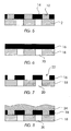
- Figs. 6-8 there is shown an alternative embodiment of the process of the present invention for making the integrated circuit devices.
- the first step of the process in this embodiment involves depositing a metallic film 16 onto a substrate 18.
- Substrate 18 is also provided with vertical metallic studs 20.
- the metallic film is lithographically patterned through a mask to form trenches 22.
- a layer 24 of dielectric composition of the present invention is deposited onto the patterned metallic film 16.
- the composition is heated to imidize the trialkoxysilylalkyl end capped polyamic ester and condense the silyl reactants.
- the dielectric layer may then be planarized for subsequent process in a multilayer integrated circuit.
- a three-neck flask equipped with an overhead stirrer, nitrogen inlet and addition funnel was charged with 9.48 mmol (3.2456 g) 3FDA, 1.04 mmol (0.2218 g) of aminophenyltrimethoxysilane, 25 mmol (2 g) of pyridine and 50 mL of distilled NMP.
- the system was continuously maintained under a positive nitrogen pressure.
- the reaction mixture was cooled to 0°C.
- the PMDA diethylester diacylchloride (10 mmol, 3.4716 g) was dissolved in ⁇ 100 mL of methylene chloride and quantitatively transferred to the addition funnel. The methylene chloride solution was added dropwise to the reaction mixture.
- the poly(amic ethyl ester) oligomer from Example 1 was dissolved in DMPU. To this solution, the polysilsequioxane (GR950F, from Techniglass) was added. A clear amber solution was formed with a solids content of 37 wt. % and a poly(amic alkyl ester) content of 23 wt. %. The solution was subsequently cast by spin coating onto glass plates to form films from 1 to 10 microns thick. The imidization was accomplished by heating the polymer films for 2 hrs each at 250° and 400°C under N 2 atmosphere. The cured polyimide films were subsequently cooled slowly to room temperature. The cured polyimide films were crack free, exhibited phase domains of 1000 ⁇ , a dielectric constant of about 2.9 at 80°C; thermal stress of about 30 mPa and a refractive index of about 1.56.
Landscapes
- Formation Of Insulating Films (AREA)
- Internal Circuitry In Semiconductor Integrated Circuit Devices (AREA)
- Silicon Polymers (AREA)
- Paints Or Removers (AREA)
- Macromolecular Compounds Obtained By Forming Nitrogen-Containing Linkages In General (AREA)
Applications Claiming Priority (2)
| Application Number | Priority Date | Filing Date | Title |
|---|---|---|---|
| US08/739,144 US5962113A (en) | 1996-10-28 | 1996-10-28 | Integrated circuit device and process for its manufacture |
| US739144 | 1996-10-28 |
Publications (2)
| Publication Number | Publication Date |
|---|---|
| EP0838853A2 true EP0838853A2 (fr) | 1998-04-29 |
| EP0838853A3 EP0838853A3 (fr) | 2000-01-05 |
Family
ID=24971025
Family Applications (1)
| Application Number | Title | Priority Date | Filing Date |
|---|---|---|---|
| EP97307999A Withdrawn EP0838853A3 (fr) | 1996-10-28 | 1997-10-09 | Circuit intégré et sa fabrication |
Country Status (8)
| Country | Link |
|---|---|
| US (1) | US5962113A (fr) |
| EP (1) | EP0838853A3 (fr) |
| JP (1) | JPH10135202A (fr) |
| KR (1) | KR100315936B1 (fr) |
| CN (1) | CN1151558C (fr) |
| MY (1) | MY118011A (fr) |
| SG (1) | SG63750A1 (fr) |
| TW (1) | TW436946B (fr) |
Cited By (4)
| Publication number | Priority date | Publication date | Assignee | Title |
|---|---|---|---|---|
| EP1085326A3 (fr) * | 1999-09-13 | 2001-08-29 | Hoya Corporation | Plaquette multicouche de circuits imprimés, procédé de fabrication et plaquette de contact pour un wafer |
| US6420441B1 (en) | 1999-10-01 | 2002-07-16 | Shipley Company, L.L.C. | Porous materials |
| US6596467B2 (en) | 2000-09-13 | 2003-07-22 | Shipley Company, L.L.C. | Electronic device manufacture |
| US6998148B1 (en) | 2001-03-28 | 2006-02-14 | Shipley Company, L.L.C. | Porous materials |
Families Citing this family (12)
| Publication number | Priority date | Publication date | Assignee | Title |
|---|---|---|---|---|
| US6323549B1 (en) | 1996-08-29 | 2001-11-27 | L. Pierre deRochemont | Ceramic composite wiring structures for semiconductor devices and method of manufacture |
| CN1171290C (zh) * | 1998-06-05 | 2004-10-13 | 佐治亚技术研究公司 | 多孔性绝缘材料及其制备方法 |
| US6143643A (en) * | 1998-07-08 | 2000-11-07 | International Business Machines Corporation | Process for manufacture of integrated circuit device using organosilicate insulative matrices |
| US6299721B1 (en) | 1998-12-14 | 2001-10-09 | Gould Electronics Incl | Coatings for improved resin dust resistance |
| US6903006B2 (en) * | 2000-03-17 | 2005-06-07 | Matsushita Electric Industrial Co., Ltd. | Interlayer dielectric film, and method for forming the same and interconnection |
| TWI226103B (en) * | 2000-08-31 | 2005-01-01 | Georgia Tech Res Inst | Fabrication of semiconductor devices with air gaps for ultra low capacitance interconnections and methods of making same |
| JP3505520B2 (ja) * | 2001-05-11 | 2004-03-08 | 松下電器産業株式会社 | 層間絶縁膜 |
| TW562822B (en) * | 2002-09-03 | 2003-11-21 | Chang Chun Plastics Co Ltd | Organic-inorganic hybrid film material and its preparation |
| WO2006109514A1 (fr) * | 2005-03-30 | 2006-10-19 | Nippon Steel Chemical Co., Ltd. | Composition de resine photosensible et substrat pour circuit l’utilisant |
| US8952119B2 (en) * | 2010-11-18 | 2015-02-10 | Aspen Aerogels, Inc. | Organically modified hybrid aerogels |
| TWI540396B (zh) * | 2014-02-18 | 2016-07-01 | 奇美實業股份有限公司 | 感光性聚矽氧烷組成物、保護膜及具有保護膜的元件 |
| CN108864711A (zh) * | 2018-06-15 | 2018-11-23 | 王娟娟 | 一种用于芯片封装的有机硅胶材料及其制备方法 |
Family Cites Families (20)
| Publication number | Priority date | Publication date | Assignee | Title |
|---|---|---|---|---|
| GB1356919A (en) * | 1970-04-17 | 1974-06-19 | Ici Ltd | Glass reinforced polymer composites |
| US3835207A (en) * | 1972-05-03 | 1974-09-10 | Westinghouse Electric Corp | Method for forming reverse osmosis membranes composed of polyamic acid salts |
| US4141877A (en) * | 1977-09-06 | 1979-02-27 | Corning Glass Works | Processing organic polymers with hydrated glasses |
| US4430153A (en) * | 1983-06-30 | 1984-02-07 | International Business Machines Corporation | Method of forming an RIE etch barrier by in situ conversion of a silicon containing alkyl polyamide/polyimide |
| US4535099A (en) * | 1984-04-03 | 1985-08-13 | Imi-Tech Corporation | Polyimide foam from mixture of silicon containing diamine and different aromatic diamine |
| US4758476A (en) * | 1984-12-12 | 1988-07-19 | Hitachi Chemical Company, Ltd. | Polyimide precursor resin composition and semiconductor device using the same |
| US4866507A (en) * | 1986-05-19 | 1989-09-12 | International Business Machines Corporation | Module for packaging semiconductor integrated circuit chips on a base substrate |
| JPH0749482B2 (ja) * | 1988-02-26 | 1995-05-31 | チッソ株式会社 | 低吸湿性かつ高接着性のシリコン含有ポリイミド及びその前駆体の製造方法 |
| US5094919A (en) * | 1988-06-30 | 1992-03-10 | Nippon Steel Chemical Co., Ltd. | Polyimide copolymers and process for preparing the same |
| US5043369A (en) * | 1988-10-17 | 1991-08-27 | Corning Incorporated | Glass/glass-ceramic-plastic alloy articles |
| JP2619515B2 (ja) * | 1989-02-02 | 1997-06-11 | チッソ株式会社 | シリコンポリイミド前駆体組成物 |
| US5036145A (en) * | 1989-07-10 | 1991-07-30 | Armstrong World Industries, Inc. | Alkoxysilane and alkoxysilane terminated polyamic or polyimide lacquer composition |
| US5206337A (en) * | 1990-05-10 | 1993-04-27 | Sumitomo Bakelite Company Limited | Solvent-soluble polyimidesiloxane oligomer and process for producing the same |
| US5288842A (en) * | 1991-01-30 | 1994-02-22 | International Business Machines Corporation | Morphological composite materials formed from different precursors |
| US5252654A (en) * | 1991-07-03 | 1993-10-12 | E. I. Du Pont De Nemours And Company | Organic-inorganic polymeric composites |
| US5412016A (en) * | 1992-09-28 | 1995-05-02 | E. I. Du Pont De Nemours And Company | Process for making polymeric inorganic-organic compositions |
| US5371047A (en) * | 1992-10-30 | 1994-12-06 | International Business Machines Corporation | Chip interconnection having a breathable etch stop layer |
| US5384376A (en) * | 1992-12-23 | 1995-01-24 | Eastman Kodak Company | Organic/inorganic hybrid materials |
| JP3395269B2 (ja) * | 1993-07-16 | 2003-04-07 | チッソ株式会社 | 低熱伝導率ポリイミドシロキサンフィルム |
| US5767014A (en) * | 1996-10-28 | 1998-06-16 | International Business Machines Corporation | Integrated circuit and process for its manufacture |
-
1996
- 1996-10-28 US US08/739,144 patent/US5962113A/en not_active Expired - Fee Related
-
1997
- 1997-06-30 KR KR1019970029756A patent/KR100315936B1/ko not_active Expired - Fee Related
- 1997-09-20 SG SG1997003478A patent/SG63750A1/en unknown
- 1997-09-26 MY MYPI97004493A patent/MY118011A/en unknown
- 1997-09-26 CN CNB971196745A patent/CN1151558C/zh not_active Expired - Fee Related
- 1997-10-09 EP EP97307999A patent/EP0838853A3/fr not_active Withdrawn
- 1997-10-15 JP JP9281641A patent/JPH10135202A/ja active Pending
-
1998
- 1998-01-23 TW TW086115875A patent/TW436946B/zh not_active IP Right Cessation
Non-Patent Citations (2)
| Title |
|---|
| J. L. HEDRICK, S. SRINIVASAN, H.-J. CHA, D. YOON, V. FLORES, M. HARBISON, R. DI PIETRO, W. HINSBERG, V. DELINE, H. R. BROWN, M. SH: "Low-Dielectric Constant Materials II. Symposium 2-3 Dec. 1996 Boston, MA,", MAT. RES. SOC. SYMP.PROC. VOL., vol. 443, 2 December 1996 (1996-12-02), Materials Research Society USA, pages 47 - 58 * |
| YOSHITAKE IYOKU, MASA-AKI KAKIMOTO, YOSHIO IMAI: "The preparation of poly(methylsilsesquioxane) network-polyimide hybrid materials by the sol-gel process and their properties", HIGH PERFORMANCE POLYMERS, vol. 6, March 1994 (1994-03-01), UK, pages 43 - 52, XP001207430 * |
Cited By (9)
| Publication number | Priority date | Publication date | Assignee | Title |
|---|---|---|---|---|
| EP1085326A3 (fr) * | 1999-09-13 | 2001-08-29 | Hoya Corporation | Plaquette multicouche de circuits imprimés, procédé de fabrication et plaquette de contact pour un wafer |
| US6492599B1 (en) | 1999-09-13 | 2002-12-10 | Hoya Corporation | Multilayer wiring board, manufacturing method thereof, and wafer block contact board |
| US6420441B1 (en) | 1999-10-01 | 2002-07-16 | Shipley Company, L.L.C. | Porous materials |
| US6602804B2 (en) | 1999-10-01 | 2003-08-05 | Shipley Company, L.L.C. | Porous materials |
| US6596467B2 (en) | 2000-09-13 | 2003-07-22 | Shipley Company, L.L.C. | Electronic device manufacture |
| US6667147B2 (en) | 2000-09-13 | 2003-12-23 | Shipley Company, L.L.C. | Electronic device manufacture |
| US7163780B2 (en) | 2000-09-13 | 2007-01-16 | Shipley Company, L.L.C. | Electronic device manufacture |
| US7294453B2 (en) | 2000-09-13 | 2007-11-13 | Shipley Company, L.L.C. | Electronic device manufacture |
| US6998148B1 (en) | 2001-03-28 | 2006-02-14 | Shipley Company, L.L.C. | Porous materials |
Also Published As
| Publication number | Publication date |
|---|---|
| KR100315936B1 (ko) | 2002-02-19 |
| CN1188987A (zh) | 1998-07-29 |
| CN1151558C (zh) | 2004-05-26 |
| MY118011A (en) | 2004-08-30 |
| US5962113A (en) | 1999-10-05 |
| JPH10135202A (ja) | 1998-05-22 |
| EP0838853A3 (fr) | 2000-01-05 |
| TW436946B (en) | 2001-05-28 |
| KR19980032201A (ko) | 1998-07-25 |
| SG63750A1 (en) | 1999-03-30 |
Similar Documents
| Publication | Publication Date | Title |
|---|---|---|
| US5883219A (en) | Integrated circuit device and process for its manufacture | |
| US5962113A (en) | Integrated circuit device and process for its manufacture | |
| US6342454B1 (en) | Electronic devices with dielectric compositions and method for their manufacture | |
| US4795680A (en) | Polyimide-siloxanes, method of making and use | |
| US5773197A (en) | Integrated circuit device and process for its manufacture | |
| US6107357A (en) | Dielectric compositions and method for their manufacture | |
| CN1142593C (zh) | 集成电路装置及其制造方法 | |
| Zhao et al. | Review of polymer materials with low dielectric constant | |
| KR900005120B1 (ko) | 반도체 장치용 절연수지조성물 및 반도체장치 | |
| KR20020094098A (ko) | 유기실리케이트 중합체의 제조방법, 및 이를 이용한절연막의 제조방법 | |
| US7608928B2 (en) | Laminated body and semiconductor device | |
| US4507333A (en) | Biphenylene end-capped quinoxaline polymers and their use as insulating coatings for semiconductor devices | |
| US5165957A (en) | Process for producing multilayer wiring structure | |
| KR19980032200A (ko) | 유전체 조성물 및 집적회로 소자 | |
| KR100508901B1 (ko) | 유기실리케이트 중합체 및 이를 함유하는 절연막 | |
| JPH0637459A (ja) | 多層配線構造の製造法 | |
| JPH05222195A (ja) | ポリイミド系樹脂前駆体の製造法および樹脂組成物 | |
| JPH06140384A (ja) | 半導体装置 | |
| CN1188988A (zh) | 电介质组合物和集成电路装置 | |
| JPS63232395A (ja) | 多層配線形成用樹脂組成物 | |
| JPH05267479A (ja) | 半導体装置の製造方法 |
Legal Events
| Date | Code | Title | Description |
|---|---|---|---|
| PUAI | Public reference made under article 153(3) epc to a published international application that has entered the european phase |
Free format text: ORIGINAL CODE: 0009012 |
|
| AK | Designated contracting states |
Kind code of ref document: A2 Designated state(s): DE FR GB |
|
| AX | Request for extension of the european patent |
Free format text: AL;LT;LV;RO;SI |
|
| PUAL | Search report despatched |
Free format text: ORIGINAL CODE: 0009013 |
|
| AK | Designated contracting states |
Kind code of ref document: A3 Designated state(s): AT BE CH DE DK ES FI FR GB GR IE IT LI LU MC NL PT SE |
|
| AX | Request for extension of the european patent |
Free format text: AL;LT;LV;RO;SI |
|
| RIC1 | Information provided on ipc code assigned before grant |
Free format text: 7H 01L 23/498 A, 7H 01L 21/48 B, 7H 01L 21/312 B, 7H 01L 23/538 B, 7C 08G 73/10 B |
|
| 17P | Request for examination filed |
Effective date: 20000516 |
|
| AKX | Designation fees paid |
Free format text: DE FR GB |
|
| 17Q | First examination report despatched |
Effective date: 20050908 |
|
| GRAP | Despatch of communication of intention to grant a patent |
Free format text: ORIGINAL CODE: EPIDOSNIGR1 |
|
| STAA | Information on the status of an ep patent application or granted ep patent |
Free format text: STATUS: THE APPLICATION IS DEEMED TO BE WITHDRAWN |
|
| 18D | Application deemed to be withdrawn |
Effective date: 20071218 |