EP0840328A2 - Procédé et dispositif pour tester circuits de mémoire - Google Patents
Procédé et dispositif pour tester circuits de mémoire Download PDFInfo
- Publication number
- EP0840328A2 EP0840328A2 EP97119055A EP97119055A EP0840328A2 EP 0840328 A2 EP0840328 A2 EP 0840328A2 EP 97119055 A EP97119055 A EP 97119055A EP 97119055 A EP97119055 A EP 97119055A EP 0840328 A2 EP0840328 A2 EP 0840328A2
- Authority
- EP
- European Patent Office
- Prior art keywords
- memory cells
- data
- state
- output
- selected memory
- Prior art date
- Legal status (The legal status is an assumption and is not a legal conclusion. Google has not performed a legal analysis and makes no representation as to the accuracy of the status listed.)
- Granted
Links
Images




Classifications
-
- G—PHYSICS
- G11—INFORMATION STORAGE
- G11C—STATIC STORES
- G11C29/00—Checking stores for correct operation ; Subsequent repair; Testing stores during standby or offline operation
- G11C29/04—Detection or location of defective memory elements, e.g. cell constructio details, timing of test signals
- G11C29/08—Functional testing, e.g. testing during refresh, power-on self testing [POST] or distributed testing
- G11C29/12—Built-in arrangements for testing, e.g. built-in self testing [BIST] or interconnection details
- G11C29/18—Address generation devices; Devices for accessing memories, e.g. details of addressing circuits
- G11C29/26—Accessing multiple arrays
-
- G—PHYSICS
- G11—INFORMATION STORAGE
- G11C—STATIC STORES
- G11C29/00—Checking stores for correct operation ; Subsequent repair; Testing stores during standby or offline operation
-
- G—PHYSICS
- G11—INFORMATION STORAGE
- G11C—STATIC STORES
- G11C29/00—Checking stores for correct operation ; Subsequent repair; Testing stores during standby or offline operation
- G11C29/04—Detection or location of defective memory elements, e.g. cell constructio details, timing of test signals
- G11C29/08—Functional testing, e.g. testing during refresh, power-on self testing [POST] or distributed testing
- G11C29/12—Built-in arrangements for testing, e.g. built-in self testing [BIST] or interconnection details
- G11C29/38—Response verification devices
- G11C29/40—Response verification devices using compression techniques
Definitions
- This invention relates in general to the field of integrated circuit memory devices, and more particularly to an integrated circuit memory device having a current-mode data compression test mode.
- Integrated circuit memory devices generally include memory arrays containing a large number of memory cells for storing data. It is important in producing such memory devices to test writing data to and reading data from the memory cells to determine whether or not there are defective memory cells in the memory device.
- Conventional processes for testing the memory cells of an integrated circuit memory device can be time consuming because of the vast number of memory cells that need to be tested. Such conventional testing processes include Writing data to the memory cells, reading data from the memory cells and checking whether the data read is the same as the data written. In general, one row of memory cells for the memory array can be tested by each read. Because of the time required, it is desirable to increase the speed with which memory cells can be tested during test mode. An architecture for increasing this speed is disclosed by U.S. Patent No. 5,305,266, issued to Rountree and entitled "High Speed Parallel Test Architecture".
- an integrated circuit memory device having a current-mode data compression test mode is provided that eliminates or reduces problems and disadvantages of prior integrated circuit memory devices.
- a memory device that has a current-mode data compression test mode.
- the memory device includes a memory array having a plurality of sub-arrays of memory cells.
- the memory cells are selected for read operations by Y-select lines and word lines.
- Selected memory cells are coupled to main amplifier circuits via bit lines, sense amplifiers, sub-input/output lines, sub-amplifier circuits, and main input/output lines.
- Each main amplifier circuit is operable, during a normal read operation, to provide a data output representing a data state of a selected memory cell.
- each main amplifier circuit is operable to provide a data output representing a data state of a plurality of selected memory cells if the plurality of selected memory cells have the same data state, and to provide an error signal if the plurality of selected memory cells have different data states.
- the test mode read operation is characterized by activating a Y-select line and a plurality of word lines to select a plurality of memory cells that are coupled to different sub-amplifier circuits that feed the same main amplifier circuit.
- a method for testing a memory device.
- a Y-select line and a plurality of word lines are activated to select a plurality of memory cells.
- the plurality of word lines are activated such that the selected memory cells are coupled to different sub-amplifier circuits that feed the same main amplifier circuit. From each main amplifier circuit, a data output representing a data state of the selected memory cells is produced if the selected memory cells have the same data state, and an error signal is produced if the selected memory cells have different data states.
- the activating and producing are repeated until all memory cells in the memory array of the memory device have been tested.
- a technical advantage of the present invention is an increase in the speed with which memory cells in a memory device can be tested by a factor of two. This increase can be realized without requiring changes to the design of the memory array in the memory device.
- Another technical advantage of the present invention is a test mode in which two rows of a memory array are simultaneously activated to place data from both rows onto common input/output lines. A three-state current-mode signal is then generated on the input/output lines that contains a data state which can be analyzed to determine whether or not the data in both rows was accurate or inaccurate.
- FIGURE 1 is a block diagram of one embodiment of an integrated circuit memory device, indicated generally at 10, having a current-mode data compression test mode. Specifically, the described embodiment is a dynamic random access memory (DRAM) device.
- FIGURE 1 shows the input/output (I/O) data path for memory device 10.
- Memory device 10 includes a number of memory sub-arrays 12 which each contain a plurality of memory cells. The memory cells within each sub-array 12 are connected to bit lines 14 and word lines 16. As shown in FIGURE 1, during a current-mode data compression test mode, two word lines 16 are active (e.g., ACTIVE WORDLINE #1 and ACTIVE WORDLINE #2).
- Memory device 10 includes a plurality of Y-select (YS) lines 18 which are used to select a particular column within memory device 10.
- Bit lines 14 are, in turn, connected to sense amplifiers 20 which are connected to sub-input/output (SIO) lines 22.
- SIO lines 22 feed sub-amplifiers 24 which connect to main input/output (MIO) lines 26, as shown.
- MIO lines 26 connect to main amplifiers 28 which can provide data output for memory device 10.
- SIO lines 22 run through the banks of sense amplifiers 20 and connect to MIO lines 26 through respective sub-amplifier circuits 24.
- MIO lines 26 are shared by many sense amplifiers 20, thus many sets of SIO lines 22 connect to each set of MIO lines 26.
- one row of memory cells in memory device 10 is activated by activating a word line 16 (e.g., WORDLINE #1). Data is then sensed in sense amplifiers 20 for that row.
- a read enable (RE) signal can be asserted to activate sub-amplifier circuits 24 for the active sense amplifiers 20.
- a YS line 18 for a particular column address can be asserted to connect selected sense amplifiers 20 to a set of SIO lines 22.
- Data is then transferred from sense amplifiers 20 to SIO lines 22 and onto MIO lines 26 through sub-amplifier circuits 24. Data on MIO lines 26 is, in turn, sensed by main amplifiers 28 located at the edge of the memory array of memory device 10.
- data can be asserted on MIO lines 26.
- a write enable (WE) signal can then be asserted to connect MIO lines 26 directly to SIO lines 22 at sub-amplifiers 24.
- a YS line 18 can then be asserted to connect data on SIO lines 22 to sense amplifiers 20.
- WE write enable
- YS line 18 can then be asserted to connect data on SIO lines 22 to sense amplifiers 20.
- a second word line (e.g., WORDLINE #2) is asserted such that two sets of sense amplifiers 20 are activated at the same time.
- the only restriction on this second word line is that the row address should not be in an adjacent sub-array 12 that shares sense amplifiers 20 and sub-amplifier circuits 24.
- RE signals are asserted for both active banks of sense amplifier 20 which connects two sub-amplifier circuits 24 to each pair of MIO lines 26.
- YS lines 18 are then asserted such that data from two banks of sense amplifiers 20 is connected to corresponding SIO lines 22 and to two active sub-amplifier circuits 24.
- sub-amplifier circuits 24 have characteristics such a three-state signal is created on MIO lines 26 depending on the data states on the active SIO lines 22.
- the signal on MIO lines 26 takes one state if the data on both active pairs of SIO lines 22 is "zero", a second state if the data on both pairs of SIO lines 22 is "one”, and a third state if there is opposite data on both pairs of SIO line 22.
- Main amplifiers 28 are designed to read this three-state signal during the current-mode data compression test mode and provide an output indicating which state is present and whether or not there is an error. By testing more than one row at a time in memory device 10, the current-mode data compression test mode reduces the time required to test the memory cells of memory device 10.
- FIGURE 2 is a circuit diagram of one embodiment of a sub-amplifier circuit 24 of memory device 10.
- sub-amplifier circuit 24 receives a pair of SIO lines 22 from a sense amplifier 20.
- SIO lines 22 include pair of lines, SIO and SIOB, which have voltage levels VSIO and VSIOB, respectively.
- the SIO line is connected to a first node, NODE 1
- the SIOB line is connected to a second node, NODE 2.
- Precharge/equalization devices 30 are connected between NODE 1 and NODE 2.
- a plurality of N-channel transistors, 32, 34, 36, 38, 40, 42 and 44 are connected, as shown.
- N-channel transistors 32, 38 and 40 are coupled to a third node, NODE 3, and receive the read enable (RE) signal.
- N-channel transistors 42 and 44 are coupled to a fifth node, NODE 5, and receive a write enable (WE) signal.
- the output of sub-amplifier circuit 24 to main amplifier 28 is provided by MIO lines 26. Similar to SIO lines 22, MIO lines 26 include an MIO and an MIOB line.
- sub-amplifier circuit 24 of FIGURE 2 provides a semi-direct sense circuit typically used in DRAM memory devices.
- a main amplifier circuit 28 located at the edge of memory device 10 can then detect this current-mode signal.
- This sub-amplifier circuit operation is summarized in the table below. TABLE 1 Sub-amplifier Circuit Operation Data in SA V SIO V SIOB I MIO I MIOB D IMIO 1 H L I 0 0 +I 0 0 L H 0 I 0 -I 0
- MIO lines 26 To write data back to SIO lines 22, data is driven on to MIO lines 26, and the WE signal is asserted high. This connects MIO lines 26 directly to SIO lines 22 through N-channel transistors 42 and 44. A YS line 18 can then be asserted such that data is transferred from SIO lines 22 into sense amplifier 20.
- FIGURE 3 is a circuit diagram of one embodiment of sub-amplifier circuit 24 operation during current-mode data compression test mode.
- two sense amplifiers 20 receive two pairs of bit lines 14 having voltage levels VBL1, VBL1B, VBL2, VBL2B.
- the two sense amplifiers 20 are selected by a YS line 18 and feed two sub-amplifier circuits 24 with SIO lines 22.
- each sub-amplifier 24 receives a write enable (WE1 and WE2) signal and a read enable (RE1 and RE2) signal.
- Sub-amplifier circuits 24 are connected to MIO lines 26 which feed a main amplifier circuit 28.
- an MIO write driver circuit 48 is connected to MIO lines 26.
- both the WE1 and WE2 signals are asserted. This connects MIO lines 26 directly to SIO lines 22 (SIO1/SIO1B and SIO2/SIO2B).
- YS line 18 is also asserted high, and data is transferred from MIO lines 26 to SIO lines 22 and to both sense amplifiers 20.
- the RE1 and RE2 signals are both asserted so that sub-amplifier circuits 24 are both connected to MIO lines 26.
- both pairs of SIO lines 22 are precharged high so that a current equal to 2I 0 flows through MIO lines 26.
- YS line 18 is then asserted, and data from the first sense amplifier 20 (SA1) is transferred to SIO1/SIO1B, and data from the second sense amplifier 20 (SA2) is transferred to SIO2/SIO2B.
- SA1 first sense amplifier 20
- SA2 second sense amplifier 20
- the final current in MIO lines 26 then depends on the data states in the two sense amplifiers 20 as shown in the table below.
- FIGURE 4 is a circuit diagram of one embodiment of a current mirror main amplifier circuit, indicated generally at 28.
- the configuration of main amplifier circuit 28 of FIGURE 4 is essentially the same as a current sensing data bus amplifier presented by FUJITSU in an article entitled "A 40-NS 64-MB DRAM with 64-B Parallel Data Bus Architecture", published in the IEEE Journal of Solid-State Circuits, Vol. 26, No. 11, November, 1991, page 1493-97.
- main amplifier 28 of FIGURE 4 is used to detect an error condition if the currents IMIO and IMIOB on MIO lines 26 are approximately equal.
- main amplifier circuit 28 receives MIO lines 26 which carry currents IMIO and IMIOB.
- a plurality of P-channel transistors 60, 62, 64, 66, 68 and 70 are connected between MIO lines 26, as shown, and create a pair of current mirror circuits.
- a plurality of N-channel transistors 72, 74, 76 and 78 are connected to the P-channel transistors, as shown, to couple together the current mirror circuits formed by the P-channel transistors.
- the P-channel and N-channel transistors of main amplifier circuit 28 are constructed such that the currents IOUT1 and IOUT2 are the same if the currents IMIO and IMIOB are the same, and the currents IOUT1 and IOUT2 are of opposite polarity if there is a difference between IMIO and IMIOB.
- Main amplifier circuit 28 then provides outputs VOUT1/IOUT1 from NODE 2 and VOUT2/IOUT2 from NODE 4 to output logic 80.
- Output logic 80 in turn provides an output data signal, DOUT and an error signal, ERROR.
- Main amplifier circuit 28 operates to produce VOUT1/IOUT1 and VOUT2/IOUT2 based upon IMIO and IMIOB on MIO lines 26.
- FIGUREs 5A and 5B are circuit diagrams of embodiments of main amplifier output logic 80.
- the embodiment of FIGURE 5A is appropriate where the value of m2 is greater than 1.
- VOUT2 is connected to the input of an inverter 82 which provides the data output, DOUT.
- VOUT2 and VOUT1 are both fed to a NOR gate 84 which provides the error signal, ERROR.
- ERROR error signal
- FIGURE 5B The embodiment of FIGURE 5B is appropriate where the value of m2 is less than 1.
- VOUT2 is connected to the input of an inverter 86 which provides the data output, DOUT.
- VOUT2 and VOUT1 are provided as inputs to a NAND gate 88 which provides its output to an inverter 90.
- the output of inverter 90 provides the error signal, ERROR. In this case, the output currents for the error condition will both be positive and produce logic highs for VOUT1 and VOUT2.
- the error signal, ERROR is ignored and the data on the differential MIO lines is converted to a single-ended data signal, DOUT.
- the error signal, ERROR will be high if an error condition exists in which opposite data is read from the two active sense amplifiers. If the error signal, ERROR, is low, then the two active sense amplifiers contain the same data state, and the DOUT signal takes the value of the data state read. This value, of course, should be compared to the expected data to ensure that both sense amplifiers do not contain incorrect data.
- the present invention allows integrated circuit memory device to be tested more quickly by testing memory cells in multiple rows at the same time.
- the testing of the memory device is an important and essential part of the manufacturing process.
- a Y-select line and a plurality of word lines are activated to select a plurality of memory cells such that the selected memory cells are coupled to different sub-amplifier circuits that feed the same main amplifier circuit.
- Each main amplifier circuit then produces a data output representing a data state of the selected memory cells if the selected memory cells have the same data state.
- Each main amplifier circuit produces an error signal if the selected memory cells have different data states.
- the activating of Y-select lines and word lines and the producing of data outputs and error signals is repeated until all memory cells in the memory array of the memory device have been tested. Memory devices that pass testing can then be separated from failed devices in order to continue the manufacturing process.
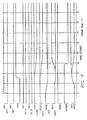
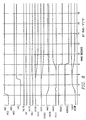
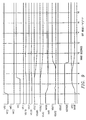
- FIGUREs 6-12 show timing diagrams for various signals for the behavior of memory device 10 shown and described with respect to FIGUREs 1-5B.
- FIGURE 6 is a timing diagram of one embodiment of read "zero" operation. This timing diagram shows the read enable signals, VRE1 and VRE2, for the two sense amplifiers (of course, only one sense amplifier is used during normal reads), and the write enable signals, VWE1 and VWE2, for those sense amplifiers.
- FIGURE 6 shows the signal on the YS line, VYS, for the memory cell being read.
- FIGURE 6 further shows: the signals on the bit lines, VBL1, VBL1B, VBL2, and VBL2B, which are sensed by the sense amplifiers; the signals on the SIO lines, VSIO1, VSIOB1, VSIO2, and VSIOB2, which are driven by the sense amplifiers; and the signals on the MIO lines, VMIO and VMIOB.
- FIGURE 6 also shows the main amplifier circuit output signals, VMIO and VMIOB, as well as the data out signal, VDOUT, and the error signal, VERROR.
- FIGURE 6 shows the current output signals if the main amplifier circuit, IMIO and IMIOB.
- FIGURE 6 shows these signals during read of a "zero" from a memory cell sensed by the first sense amplifier.
- FIGURE 7 is a timing diagram of one embodiment of read “one” operation.
- FIGURE 7 shows the same signals as FIGURE 6 but with a "one" being read from the first sense amplifier.
- FIGURE 8 is a timing diagram of one embodiment of current-mode data compression test mode operation with "zero" in both sense amplifiers
- FIGURE 9 is a timing diagram of one embodiment of current-mode data compression test mode operation with a "one" in both sense amplifiers.
- FIGUREs 8 and 9 show the same set of signals discussed above in the situation where the two memory cells being tested hold the same data states as expected.
- FIGURE 10 is a timing diagram of one embodiment of current-mode data compression test mode operation with a "zero" in a first sense amplifier and a “one” in a second sense amplifier
- FIGURE 11 is a timing diagram of one embodiment of current-mode data compression test mode operation with a "one" in a first sense amplifier and a “zero” in a second sense amplifier.
- FIGUREs 10 and 11 show the same set of signals. However, in FIGUREs 10 and 11, the two memory cells being tested hold different data states, thus an error is indicated by error signal, VERROR.
- FIGURE 12 is a timing diagram of one embodiment of current-mode data compression test mode write operation.
- FIGURE 12 shows the same set of signals in the situation where data is being written to the memory cells connected to two sense amplifiers. The same data can be written to the cells accessed by two word lines, and then those cells can be tested as discussed above.
- the current-mode data compression test scheme provided herein allows for a multiple reduction in the number of row addresses that need to be accessed in order to test an entire memory array.
- this test mode can be implemented on a memory device without changing the architecture or layout of the memory array in the memory device.
Landscapes
- For Increasing The Reliability Of Semiconductor Memories (AREA)
- Dram (AREA)
- Testing Or Measuring Of Semiconductors Or The Like (AREA)
- Tests Of Electronic Circuits (AREA)
Applications Claiming Priority (2)
| Application Number | Priority Date | Filing Date | Title |
|---|---|---|---|
| US2941996P | 1996-10-31 | 1996-10-31 | |
| US29419P | 1996-10-31 |
Publications (3)
| Publication Number | Publication Date |
|---|---|
| EP0840328A2 true EP0840328A2 (fr) | 1998-05-06 |
| EP0840328A3 EP0840328A3 (fr) | 1999-05-12 |
| EP0840328B1 EP0840328B1 (fr) | 2003-09-10 |
Family
ID=21848922
Family Applications (1)
| Application Number | Title | Priority Date | Filing Date |
|---|---|---|---|
| EP97119055A Expired - Lifetime EP0840328B1 (fr) | 1996-10-31 | 1997-10-31 | Procédé et dispositif pour tester circuits de mémoire |
Country Status (5)
| Country | Link |
|---|---|
| EP (1) | EP0840328B1 (fr) |
| JP (1) | JPH10283798A (fr) |
| KR (1) | KR100494281B1 (fr) |
| DE (1) | DE69724737T2 (fr) |
| TW (1) | TW406268B (fr) |
Cited By (7)
| Publication number | Priority date | Publication date | Assignee | Title |
|---|---|---|---|---|
| WO1999005682A1 (fr) * | 1997-07-24 | 1999-02-04 | Micron Technology, Inc. | Procede et appareil permettant de lire des donnees d'essai comprimees dans des dispositifs a memoire |
| WO1999005782A3 (fr) * | 1997-07-24 | 1999-04-15 | Micron Technology Inc | Amplificateur de detection pour signaux de donnees complementaires ou non complementaires |
| US5935263A (en) * | 1997-07-01 | 1999-08-10 | Micron Technology, Inc. | Method and apparatus for memory array compressed data testing |
| US6032274A (en) * | 1997-06-20 | 2000-02-29 | Micron Technology, Inc. | Method and apparatus for compressed data testing of more than one memory array |
| US6115303A (en) * | 1998-10-09 | 2000-09-05 | Micron Technology, Inc. | Method and apparatus for testing memory devices |
| US6295618B1 (en) | 1998-08-25 | 2001-09-25 | Micron Technology, Inc. | Method and apparatus for data compression in memory devices |
| US7248516B2 (en) * | 2001-02-27 | 2007-07-24 | Micron Technology, Inc. | Data compression read mode for memory testing |
Families Citing this family (3)
| Publication number | Priority date | Publication date | Assignee | Title |
|---|---|---|---|---|
| JP4632107B2 (ja) * | 2000-06-29 | 2011-02-16 | エルピーダメモリ株式会社 | 半導体記憶装置 |
| KR100634165B1 (ko) * | 2003-06-17 | 2006-10-16 | 삼성전자주식회사 | 칩 면적의 증가없이 입출력 라인들의 수를 증가시킬 수있는 반도체 메모리 장치 |
| KR20210085994A (ko) | 2019-12-31 | 2021-07-08 | 전북대학교산학협력단 | 금속황화물(Metal sulfide)과 전기화학적 반응을 통한 활성산소종(Reactive oxygen species) 제조방법 및 이를 활용한 산화처리 기술 |
Family Cites Families (3)
| Publication number | Priority date | Publication date | Assignee | Title |
|---|---|---|---|---|
| JPS63244399A (ja) * | 1987-03-16 | 1988-10-11 | シーメンス・アクチエンゲゼルシヤフト | 半導体メモリの検査方法および回路装置 |
| GB2222461B (en) * | 1988-08-30 | 1993-05-19 | Mitsubishi Electric Corp | On chip testing of semiconductor memory devices |
| GB2256279B (en) * | 1988-08-30 | 1993-05-12 | Mitsubishi Electric Corp | Semiconductor memory device |
-
1997
- 1997-10-30 KR KR1019970056417A patent/KR100494281B1/ko not_active Expired - Lifetime
- 1997-10-31 DE DE69724737T patent/DE69724737T2/de not_active Expired - Lifetime
- 1997-10-31 JP JP9337641A patent/JPH10283798A/ja active Pending
- 1997-10-31 EP EP97119055A patent/EP0840328B1/fr not_active Expired - Lifetime
- 1997-11-11 TW TW086116303A patent/TW406268B/zh not_active IP Right Cessation
Cited By (17)
| Publication number | Priority date | Publication date | Assignee | Title |
|---|---|---|---|---|
| US6032274A (en) * | 1997-06-20 | 2000-02-29 | Micron Technology, Inc. | Method and apparatus for compressed data testing of more than one memory array |
| US5935263A (en) * | 1997-07-01 | 1999-08-10 | Micron Technology, Inc. | Method and apparatus for memory array compressed data testing |
| WO1999005682A1 (fr) * | 1997-07-24 | 1999-02-04 | Micron Technology, Inc. | Procede et appareil permettant de lire des donnees d'essai comprimees dans des dispositifs a memoire |
| WO1999005782A3 (fr) * | 1997-07-24 | 1999-04-15 | Micron Technology Inc | Amplificateur de detection pour signaux de donnees complementaires ou non complementaires |
| US5959921A (en) * | 1997-07-24 | 1999-09-28 | Micron Technology, Inc. | Sense amplifier for complement or no-complementary data signals |
| US6005816A (en) * | 1997-07-24 | 1999-12-21 | Micron Technology, Inc. | Sense amplifier for complementary or non-complementary data signals |
| US6055654A (en) * | 1997-07-24 | 2000-04-25 | Micron Technology, Inc. | Method and apparatus for reading compressed test data from memory devices |
| US6987702B2 (en) | 1998-08-25 | 2006-01-17 | Mycron Technology, Inc. | Method and apparatus for data compression in memory devices |
| US6295618B1 (en) | 1998-08-25 | 2001-09-25 | Micron Technology, Inc. | Method and apparatus for data compression in memory devices |
| US6819611B2 (en) | 1998-08-25 | 2004-11-16 | Micron Technology, Inc. | Method and apparatus for data compression in memory devices |
| US6999361B2 (en) | 1998-08-25 | 2006-02-14 | Micron Technology, Inc. | Method and apparatus for data compression in memory devices |
| US7136316B2 (en) | 1998-08-25 | 2006-11-14 | Micron Technology, Inc. | Method and apparatus for data compression in memory devices |
| US7190625B2 (en) | 1998-08-25 | 2007-03-13 | Micron Technology, Inc. | Method and apparatus for data compression in memory devices |
| US6252811B1 (en) | 1998-10-09 | 2001-06-26 | Micron Technology, Inc. | Method and apparatus for testing memory devices |
| US6327199B1 (en) | 1998-10-09 | 2001-12-04 | Micron Technology, Inc. | Method for testing memory devices |
| US6115303A (en) * | 1998-10-09 | 2000-09-05 | Micron Technology, Inc. | Method and apparatus for testing memory devices |
| US7248516B2 (en) * | 2001-02-27 | 2007-07-24 | Micron Technology, Inc. | Data compression read mode for memory testing |
Also Published As
| Publication number | Publication date |
|---|---|
| TW406268B (en) | 2000-09-21 |
| EP0840328A3 (fr) | 1999-05-12 |
| DE69724737T2 (de) | 2004-08-05 |
| DE69724737D1 (de) | 2003-10-16 |
| JPH10283798A (ja) | 1998-10-23 |
| KR19980033332A (ko) | 1998-07-25 |
| KR100494281B1 (ko) | 2005-08-05 |
| EP0840328B1 (fr) | 2003-09-10 |
Similar Documents
| Publication | Publication Date | Title |
|---|---|---|
| JP2673395B2 (ja) | 半導体記憶装置およびそのテスト方法 | |
| US6819611B2 (en) | Method and apparatus for data compression in memory devices | |
| US5926422A (en) | Integrated circuit memory device having current-mode data compression test mode | |
| JPH04356799A (ja) | 半導体記憶装置 | |
| US7088624B2 (en) | System of multiplexed data lines in a dynamic random access memory | |
| EP0840328B1 (fr) | Procédé et dispositif pour tester circuits de mémoire | |
| JP3484388B2 (ja) | 半導体記憶装置 | |
| US7002258B2 (en) | Dual port memory core cell architecture with matched bit line capacitances | |
| US6363001B1 (en) | ROM with a reduced static consumption | |
| EP0634751B1 (fr) | Procédé et appareil pour test en parallèle de mémoires | |
| US7079427B2 (en) | System and method for a high-speed access architecture for semiconductor memory | |
| JPH09259600A (ja) | 半導体記憶装置 | |
| US6330198B1 (en) | Semiconductor storage device | |
| EP0640917A2 (fr) | Circuit roll call pour mémoire à semi-conducteur | |
| JPH0589700A (ja) | 高速並列テストの機構 | |
| US6975548B2 (en) | Memory device having redundant memory cell | |
| RU2084972C1 (ru) | Способ записи данных при тестировании устройства памяти и устройство для проверки памяти | |
| US7436720B2 (en) | Semiconductor memory device | |
| US6134159A (en) | Semiconductor memory and redundant circuit | |
| US6002616A (en) | Reference voltage generating circuit of sense amplifier using residual data line | |
| JP3106686B2 (ja) | 半導体記憶装置 | |
| JPH0581899A (ja) | 半導体記憶装置 | |
| JP3050704B2 (ja) | 半導体メモリ装置 | |
| JPS63140499A (ja) | 半導体記憶装置 | |
| JPH0581897A (ja) | 半導体記憶装置 |
Legal Events
| Date | Code | Title | Description |
|---|---|---|---|
| PUAI | Public reference made under article 153(3) epc to a published international application that has entered the european phase |
Free format text: ORIGINAL CODE: 0009012 |
|
| AK | Designated contracting states |
Kind code of ref document: A2 Designated state(s): DE FR GB IT NL |
|
| AX | Request for extension of the european patent |
Free format text: AL;LT;LV;RO;SI |
|
| PUAL | Search report despatched |
Free format text: ORIGINAL CODE: 0009013 |
|
| AK | Designated contracting states |
Kind code of ref document: A3 Designated state(s): AT BE CH DE DK ES FI FR GB GR IE IT LI LU MC NL PT SE |
|
| AX | Request for extension of the european patent |
Free format text: AL;LT;LV;RO;SI |
|
| 17P | Request for examination filed |
Effective date: 19991104 |
|
| AKX | Designation fees paid |
Free format text: DE FR GB IT NL |
|
| 17Q | First examination report despatched |
Effective date: 20020122 |
|
| GRAH | Despatch of communication of intention to grant a patent |
Free format text: ORIGINAL CODE: EPIDOS IGRA |
|
| GRAS | Grant fee paid |
Free format text: ORIGINAL CODE: EPIDOSNIGR3 |
|
| GRAA | (expected) grant |
Free format text: ORIGINAL CODE: 0009210 |
|
| AK | Designated contracting states |
Kind code of ref document: B1 Designated state(s): DE FR GB IT NL |
|
| PG25 | Lapsed in a contracting state [announced via postgrant information from national office to epo] |
Ref country code: NL Free format text: LAPSE BECAUSE OF FAILURE TO SUBMIT A TRANSLATION OF THE DESCRIPTION OR TO PAY THE FEE WITHIN THE PRESCRIBED TIME-LIMIT Effective date: 20030910 Ref country code: IT Free format text: LAPSE BECAUSE OF FAILURE TO SUBMIT A TRANSLATION OF THE DESCRIPTION OR TO PAY THE FEE WITHIN THE PRESCRIBED TIME-LIMIT;WARNING: LAPSES OF ITALIAN PATENTS WITH EFFECTIVE DATE BEFORE 2007 MAY HAVE OCCURRED AT ANY TIME BEFORE 2007. THE CORRECT EFFECTIVE DATE MAY BE DIFFERENT FROM THE ONE RECORDED. Effective date: 20030910 |
|
| REG | Reference to a national code |
Ref country code: GB Ref legal event code: FG4D |
|
| REF | Corresponds to: |
Ref document number: 69724737 Country of ref document: DE Date of ref document: 20031016 Kind code of ref document: P |
|
| NLV1 | Nl: lapsed or annulled due to failure to fulfill the requirements of art. 29p and 29m of the patents act | ||
| ET | Fr: translation filed | ||
| PLBE | No opposition filed within time limit |
Free format text: ORIGINAL CODE: 0009261 |
|
| STAA | Information on the status of an ep patent application or granted ep patent |
Free format text: STATUS: NO OPPOSITION FILED WITHIN TIME LIMIT |
|
| 26N | No opposition filed |
Effective date: 20040614 |
|
| PGFP | Annual fee paid to national office [announced via postgrant information from national office to epo] |
Ref country code: GB Payment date: 20120925 Year of fee payment: 16 |
|
| PGFP | Annual fee paid to national office [announced via postgrant information from national office to epo] |
Ref country code: DE Payment date: 20121031 Year of fee payment: 16 Ref country code: FR Payment date: 20121010 Year of fee payment: 16 |
|
| GBPC | Gb: european patent ceased through non-payment of renewal fee |
Effective date: 20131031 |
|
| PG25 | Lapsed in a contracting state [announced via postgrant information from national office to epo] |
Ref country code: GB Free format text: LAPSE BECAUSE OF NON-PAYMENT OF DUE FEES Effective date: 20131031 |
|
| REG | Reference to a national code |
Ref country code: DE Ref legal event code: R119 Ref document number: 69724737 Country of ref document: DE Effective date: 20140501 |
|
| REG | Reference to a national code |
Ref country code: FR Ref legal event code: ST Effective date: 20140630 |
|
| PG25 | Lapsed in a contracting state [announced via postgrant information from national office to epo] |
Ref country code: DE Free format text: LAPSE BECAUSE OF NON-PAYMENT OF DUE FEES Effective date: 20140501 Ref country code: FR Free format text: LAPSE BECAUSE OF NON-PAYMENT OF DUE FEES Effective date: 20131031 |