EP0841733A1 - Dispositif optique à semi-conducteur et méthode de communication - Google Patents
Dispositif optique à semi-conducteur et méthode de communication Download PDFInfo
- Publication number
- EP0841733A1 EP0841733A1 EP97119465A EP97119465A EP0841733A1 EP 0841733 A1 EP0841733 A1 EP 0841733A1 EP 97119465 A EP97119465 A EP 97119465A EP 97119465 A EP97119465 A EP 97119465A EP 0841733 A1 EP0841733 A1 EP 0841733A1
- Authority
- EP
- European Patent Office
- Prior art keywords
- region
- bias voltage
- semiconductor optical
- light
- functional device
- Prior art date
- Legal status (The legal status is an assumption and is not a legal conclusion. Google has not performed a legal analysis and makes no representation as to the accuracy of the status listed.)
- Granted
Links
- 239000004065 semiconductor Substances 0.000 title claims abstract description 113
- 230000003287 optical effect Effects 0.000 title claims abstract description 75
- 238000000034 method Methods 0.000 title claims description 13
- 230000010287 polarization Effects 0.000 claims description 42
- 230000003321 amplification Effects 0.000 claims description 13
- 238000003199 nucleic acid amplification method Methods 0.000 claims description 13
- 239000013307 optical fiber Substances 0.000 description 7
- 230000010355 oscillation Effects 0.000 description 7
- 238000004891 communication Methods 0.000 description 6
- 230000005684 electric field Effects 0.000 description 5
- 239000000758 substrate Substances 0.000 description 3
- 230000005540 biological transmission Effects 0.000 description 2
- 238000006243 chemical reaction Methods 0.000 description 2
- 238000005253 cladding Methods 0.000 description 2
- 238000007796 conventional method Methods 0.000 description 1
- 230000003247 decreasing effect Effects 0.000 description 1
- 230000000694 effects Effects 0.000 description 1
- 238000005530 etching Methods 0.000 description 1
- 238000001914 filtration Methods 0.000 description 1
- 239000000463 material Substances 0.000 description 1
- 238000012986 modification Methods 0.000 description 1
- 230000004048 modification Effects 0.000 description 1
- 238000000206 photolithography Methods 0.000 description 1
- 238000012545 processing Methods 0.000 description 1
Images



Classifications
-
- H—ELECTRICITY
- H01—ELECTRIC ELEMENTS
- H01S—DEVICES USING THE PROCESS OF LIGHT AMPLIFICATION BY STIMULATED EMISSION OF RADIATION [LASER] TO AMPLIFY OR GENERATE LIGHT; DEVICES USING STIMULATED EMISSION OF ELECTROMAGNETIC RADIATION IN WAVE RANGES OTHER THAN OPTICAL
- H01S5/00—Semiconductor lasers
- H01S5/50—Amplifier structures not provided for in groups H01S5/02 - H01S5/30
- H01S5/5009—Amplifier structures not provided for in groups H01S5/02 - H01S5/30 the arrangement being polarisation-insensitive
-
- B—PERFORMING OPERATIONS; TRANSPORTING
- B82—NANOTECHNOLOGY
- B82Y—SPECIFIC USES OR APPLICATIONS OF NANOSTRUCTURES; MEASUREMENT OR ANALYSIS OF NANOSTRUCTURES; MANUFACTURE OR TREATMENT OF NANOSTRUCTURES
- B82Y20/00—Nanooptics, e.g. quantum optics or photonic crystals
-
- H—ELECTRICITY
- H01—ELECTRIC ELEMENTS
- H01S—DEVICES USING THE PROCESS OF LIGHT AMPLIFICATION BY STIMULATED EMISSION OF RADIATION [LASER] TO AMPLIFY OR GENERATE LIGHT; DEVICES USING STIMULATED EMISSION OF ELECTROMAGNETIC RADIATION IN WAVE RANGES OTHER THAN OPTICAL
- H01S5/00—Semiconductor lasers
- H01S5/06—Arrangements for controlling the laser output parameters, e.g. by operating on the active medium
- H01S5/0607—Arrangements for controlling the laser output parameters, e.g. by operating on the active medium by varying physical parameters other than the potential of the electrodes, e.g. by an electric or magnetic field, mechanical deformation, pressure, light, temperature
- H01S5/0608—Arrangements for controlling the laser output parameters, e.g. by operating on the active medium by varying physical parameters other than the potential of the electrodes, e.g. by an electric or magnetic field, mechanical deformation, pressure, light, temperature controlled by light, e.g. optical switch
- H01S5/0609—Arrangements for controlling the laser output parameters, e.g. by operating on the active medium by varying physical parameters other than the potential of the electrodes, e.g. by an electric or magnetic field, mechanical deformation, pressure, light, temperature controlled by light, e.g. optical switch acting on an absorbing region, e.g. wavelength convertors
-
- H—ELECTRICITY
- H01—ELECTRIC ELEMENTS
- H01S—DEVICES USING THE PROCESS OF LIGHT AMPLIFICATION BY STIMULATED EMISSION OF RADIATION [LASER] TO AMPLIFY OR GENERATE LIGHT; DEVICES USING STIMULATED EMISSION OF ELECTROMAGNETIC RADIATION IN WAVE RANGES OTHER THAN OPTICAL
- H01S2301/00—Functional characteristics
- H01S2301/14—Semiconductor lasers with special structural design for lasing in a specific polarisation mode
-
- H—ELECTRICITY
- H01—ELECTRIC ELEMENTS
- H01S—DEVICES USING THE PROCESS OF LIGHT AMPLIFICATION BY STIMULATED EMISSION OF RADIATION [LASER] TO AMPLIFY OR GENERATE LIGHT; DEVICES USING STIMULATED EMISSION OF ELECTROMAGNETIC RADIATION IN WAVE RANGES OTHER THAN OPTICAL
- H01S5/00—Semiconductor lasers
- H01S5/06—Arrangements for controlling the laser output parameters, e.g. by operating on the active medium
- H01S5/062—Arrangements for controlling the laser output parameters, e.g. by operating on the active medium by varying the potential of the electrodes
- H01S5/06233—Controlling other output parameters than intensity or frequency
- H01S5/06236—Controlling other output parameters than intensity or frequency controlling the polarisation, e.g. TM/TE polarisation switching
-
- H—ELECTRICITY
- H01—ELECTRIC ELEMENTS
- H01S—DEVICES USING THE PROCESS OF LIGHT AMPLIFICATION BY STIMULATED EMISSION OF RADIATION [LASER] TO AMPLIFY OR GENERATE LIGHT; DEVICES USING STIMULATED EMISSION OF ELECTROMAGNETIC RADIATION IN WAVE RANGES OTHER THAN OPTICAL
- H01S5/00—Semiconductor lasers
- H01S5/06—Arrangements for controlling the laser output parameters, e.g. by operating on the active medium
- H01S5/062—Arrangements for controlling the laser output parameters, e.g. by operating on the active medium by varying the potential of the electrodes
- H01S5/0625—Arrangements for controlling the laser output parameters, e.g. by operating on the active medium by varying the potential of the electrodes in multi-section lasers
-
- H—ELECTRICITY
- H01—ELECTRIC ELEMENTS
- H01S—DEVICES USING THE PROCESS OF LIGHT AMPLIFICATION BY STIMULATED EMISSION OF RADIATION [LASER] TO AMPLIFY OR GENERATE LIGHT; DEVICES USING STIMULATED EMISSION OF ELECTROMAGNETIC RADIATION IN WAVE RANGES OTHER THAN OPTICAL
- H01S5/00—Semiconductor lasers
- H01S5/10—Construction or shape of the optical resonator, e.g. extended or external cavity, coupled cavities, bent-guide, varying width, thickness or composition of the active region
- H01S5/1053—Comprising an active region having a varying composition or cross-section in a specific direction
- H01S5/1057—Comprising an active region having a varying composition or cross-section in a specific direction varying composition along the optical axis
-
- H—ELECTRICITY
- H01—ELECTRIC ELEMENTS
- H01S—DEVICES USING THE PROCESS OF LIGHT AMPLIFICATION BY STIMULATED EMISSION OF RADIATION [LASER] TO AMPLIFY OR GENERATE LIGHT; DEVICES USING STIMULATED EMISSION OF ELECTROMAGNETIC RADIATION IN WAVE RANGES OTHER THAN OPTICAL
- H01S5/00—Semiconductor lasers
- H01S5/30—Structure or shape of the active region; Materials used for the active region
- H01S5/34—Structure or shape of the active region; Materials used for the active region comprising quantum well or superlattice structures, e.g. single quantum well [SQW] lasers, multiple quantum well [MQW] lasers or graded index separate confinement heterostructure [GRINSCH] lasers
- H01S5/3403—Structure or shape of the active region; Materials used for the active region comprising quantum well or superlattice structures, e.g. single quantum well [SQW] lasers, multiple quantum well [MQW] lasers or graded index separate confinement heterostructure [GRINSCH] lasers having a strained layer structure in which the strain performs a special function, e.g. general strain effects, strain versus polarisation
- H01S5/3404—Structure or shape of the active region; Materials used for the active region comprising quantum well or superlattice structures, e.g. single quantum well [SQW] lasers, multiple quantum well [MQW] lasers or graded index separate confinement heterostructure [GRINSCH] lasers having a strained layer structure in which the strain performs a special function, e.g. general strain effects, strain versus polarisation influencing the polarisation
Definitions
- the present invention relates to a semiconductor optical functional device, and particularly to an optical functional device which is used for an optical fiber communication system and is capable of performing mode conversion, mode filtering, or optical amplification with respect to a TE mode and a TM mode which are polarization modes in which light orthogonally intersects.
- an optical isolator is generally employed to remove the light returning to the semiconductor laser.
- the optical isolator is used to remove the returning light to the semiconductor laser.
- the optical isolator requires a number of steps for processing and assembling materials, and is not only expensive but also poor in reliability and stability.
- the optical isolator is used for an optical fiber communication system, there arises a problem that the reliability and stability of the whole system are damaged.
- the present invention has been made in view of the above described problem possessed by the conventional technique, and an object thereof is therefore to provide a semiconductor optical functional device which is capable of removing returning light to a semiconductor laser without using an optical isolator.
- a semiconductor optical functional device is constituted by two regions of a first region and a second region adjacent to each other in a longitudinal direction of a semiconductor optical waveguide, and is characterized in that the first region has an MQW (Multiple Quantum Well) structure in which a compressive strain is introduced to a well, and the second region has an MQW structure in which a tensile strain is introduced to a well.
- MQW Multiple Quantum Well
- the first region and the second region are provided with electrodes formed separately and independently from each other, and the first region and the second region perform an amplifying operation when a forward bias voltage is applied to the electrodes, and perform an absorbing operation when a reverse bias voltage is applied to the electrodes.
- a method of driving the semiconductor optical functional device of the second aspect is characterized in that a reverse bias voltage is applied to the electrode disposed on the first region; and a forward bias voltage is applied to the electrode disposed on the second region, whereby when light having a TE mode component is inputted into the first region, the semiconductor optical functional device is driven as a semiconductor integrated polarization mode converter which converts the incident light into light having a TM mode component and outputs the converted light.
- a method of driving the semiconductor optical functional device of the second aspect is characterized in that a forward bias voltage is applied to the electrode disposed on the first region; and a reverse bias voltage is applied to the electrode disposed on the second region, whereby when light having a TM mode component is inputted into the first region, the semiconductor optical functional device is driven as a semiconductor integrated polarization mode converter which converts the incident light into light having a TE mode component and outputs the converted light.
- a method of driving the semiconductor optical functional device of the second aspect is characterized in that a reverse bias voltage is applied to the electrode disposed on the first region; and a forward bias voltage is applied to the electrode disposed on the second region, the forward bias voltage being so small that laser oscillation does not occur in the second region, whereby when light having a TE mode component and a TM mode component is inputted into the first region, the semiconductor optical functional device is driven as a semiconductor integrated polarization mode filter which makes only the light having the TM mode component pass through and outputs the passed light.
- a method of driving the semiconductor optical functional device of the second aspect is characterized in that a forward bias voltage is applied to the electrode disposed on the first region, the forward bias voltage being so small that laser oscillation does not occur in the first region; and a reverse bias voltage is applied to the electrode disposed on the second region, whereby when light having a TE mode component and a TM mode component is inputted into the first region, the semiconductor optical functional device is driven as a semiconductor integrated polarization mode filter which makes only the light having the TE mode component pass through and outputs the passed light.
- a method of driving the semiconductor optical functional device is characterized in that adjusted forward bias voltages are respectively applied to the electrodes disposed on the first region and the second region, whereby when light having a TE mode component and a TM mode component is inputted into the first region, the semiconductor optical functional device is driven as an integrated polarization mode independent amplification semiconductor optical amplifier which controls the respective gains of the TE mode component and the TM mode component independently to output light from the second region.
- Figs. 1A and 1B are views for explaining the operation principle in the case where the semiconductor optical functional device of the present invention is activated as the semiconductor integrated polarization mode converter, Fig. 1A being a sectional view showing the structure thereof, and Fig. 1B being a view showing the dependency of oscillator net gain and power of TM mode light which is to be oscillated, with respect to input power of TE mode light.
- the structure of the semiconductor integrated polarization mode converter is the same as that of a semiconductor laser including a multiple oscillator structure. That is, an oscillator using a normal laser is divided into two regions of a first region and a second region adjacent to each other in a longitudinal direction of a semiconductor optical waveguide.
- the first region 1 is provided with a region having an MQW structure in which a compressive strain is introduced into a well
- the second region 2 is provided with a region having an MQW structure in which a tensile strain is introduced into a well.
- electrodes 3 and 4 formed separately and independently from each other are disposed on the first region 1 and the second region 2, respectively.
- the region performs an amplifying or absorbing operation with respect to light of the TE mode.
- the tensile strain MQW since the first level of a valence band thereof is an LH band, the region performs an amplifying or absorbing operation with respect to light of the TM mode. Whether the amplifying operation is performed or absorbing operation is performed, is controlled by a voltage applied to the electrodes provided on the respective regions. When the voltage applied to the electrode is a forward bias voltage, the amplifying operation is performed, and when the applied voltage is a reverse bias voltage, the absorbing operation is performed.
- the forward bias voltage is applied to the second region having the tensile strain MQW structure, and light having the TE mode component is inputted into the first region 1.
- the incident light having the TE mode component is absorbed in the region having the compressive strain MQW structure in the first region 1, so that the loss of a multiple oscillator is decreased, and the net gain is increased.
- the net gain exceeds a threshold gain, light having the TM mode component is oscillated from the region having the tensile strain MQW structure in the second region 2, so that emitted light having the TM mode component is obtained.
- the incident light having the TE mode component is converted into the light having the TM mode component.
- Figs. 2A and 2B are views for explaining the operation principle in the case where a semiconductor optical functional device of the present invention is activated as the semiconductor integrated polarization mode filter, Fig. 2A being a sectional view showing the structure thereof, and Fig. 2B being a view showing the distribution of electric field in the respective TE mode and TM mode.
- the structure of the semiconductor integrated polarization mode filter is the same as that of the semiconductor integrated polarization converter as shown in Fig. 1A.
- a forward bias voltage applied to the first region 1 or the second region 2 is made so small that laser oscillation does not occur in the region to which the forward bias is applied.
- a forward bias voltage which is so small that laser oscillation is not caused, is applied to the second region 2 having the tensile strain MQW structure, and light having two mode components of TE and TM is inputted into the first region 1, as shown in Fig. 2B, in the TE mode component and the TM mode component of the incident light, the TE mode component is absorbed in the region having the compressive strain MQW structure in the first region 1, and only light having the TM mode component is emitted from the region having the tensile strain MQW structure in the second region 2.
- a forward bias voltage which is so small that laser oscillation is not caused
- a reverse bias voltage is applied to the second region 2 having the tensile strain MQW structure, and light having two mode components of TE and TM is inputted into the first region 1, in the TE mode component and the TM mode component of the incident light, the TM mode component is absorbed in the region having the tensile strain MQW structure in the second region 2, and only light having the TE mode component is emitted from the region having the tensile strain MQW structure in the second region 2.
- the semiconductor optical functional device of the present invention can also be activated as the semiconductor integrated polarization mode filter for selectively removing the TE mode component or TM mode component of the incident light.
- Figs. 3A and 3B are views for explaining the operation principle in the case where a semiconductor optical functional device of the present invention is activated as the integrated polarization mode independent amplification semiconductor amplifier, Fig 3A being a sectional view showing the structure thereof, and Fig. 3B being a view showing the distribution of electric field in the respective TE mode and TM mode.
- the structure of the integrated polarization mode independent amplification semiconductor optical amplifier is the same as that of the semiconductor integrated polarization converter shown in Fig. 1A.
- forward bias voltages are applied to the first region 1 and the second region 2, and the bias voltages applied to the respective regions are adjusted so that gains of the respective TE mode and TM mode can be independently controlled.
- the light power of the TE mode and TM mode of the incident light is respectively amplified in the gain regions of the first region 1 and the second region 2, so that the semiconductor optical functional device functions as the integrated polarization mode independent amplification semiconductor optical amplifier.
- Figs. 4A and 4B are views showing an embodiment in which a semiconductor optical functional device of the present invention is used as a semiconductor integrated polarization mode converter
- Fig. 4A being a sectional view showing an example in which light of a TE mode component is converted into light of a TM mode component
- Fig 4B being a view showing an example in which light of the TM mode component is converted into light of the TE mode component.
- an InGaAsP cladding layer 22 is grown on an InP substrate 21, and then a compressive strain MQW structure and a tensile strain MQW structure adjacent to each other are formed by carrying out selective growth two times.
- the InGaAsP cladding layer 22 and the InP substrate 21 are subjected to embedded growth and a ridge waveguide with a width of 2 ⁇ m is formed by normal photolithography and etching.
- a whole surface electrode 15 is formed on the lower surface of the InP substrate 21, and electrodes 13 and 14 independent from each other are formed on the upper surface of the semiconductor device which is divided into a first region 11 having the compressive strain MQW structure and a second region 2 having the tensile strain MQW structure.
- an electric current is injected into the second region 12 having the tensile strain MQW structure, and a reverse bias voltage is applied to the first region 11 having the compressive strain MQW, so that the TE mode can be converted into the TM mode as shown in Fig. 4A.
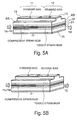
- Figs. 5A and 5B are views showing an embodiment in which a semiconductor optical functional device of the present invention is used as an integrated polarization mode filter.
- Fig. 5A is a view showing an example in which when light of the TE mode component and TM mode component is inputted, only light of the TM mode component is emitted
- Fig. 5B is a view showing an example in which when light of the TE mode component and TM mode component is inputted, only light of the TE mode component is emitted.
- AR films 23 are deposited to the structure shown in Figs. 4A and 4B, and the value of forward bias voltage applied to the first region 11 or the second region 12 is made so small that laser oscillation does not occur in the region where the forward bias voltage is applied.
- the semiconductor device functions as the semiconductor integrated polarization mode filter.
- Fig. 6 is a view showing an embodiment in the case where a semiconductor optical functional device of the present invention is used as an integrated polarization mode independent amplification semiconductor amplifier.
- forward bias voltages are applied to both a first region 11 having a compressive strain MQW structure and a second region 12 having a tensile strain MQW structure, and the bias voltages applied to the respective regions are adjusted so that gains of the TE mode and TM mode are independently controlled. Accordingly, the semiconductor device functions as the integrated polarization mode independent amplification semiconductor amplifier.
- the present invention is structured as described above, so that the following effects can be obtained.
- the region having the compressive strain MQW structure is disposed in the first region, and the region having the tensile strain MQW structure is disposed in the second region, so that the semiconductor optical functional device is capable of independently controlling transmissivities for the light having the TE mode component and the light having the TM mode component.
- bias voltages different from each other are applied to the electrodes disposed on the first region and the second region, so that the semiconductor optical functional device can be driven as the semiconductor integrated polarization mode converter which converts the component of incident light and outputs the converted light.
- bias voltages different from each other are applied to the electrodes disposed on the first region and the second region, and in the application of the forward bias voltage, the bias voltage is made so small that laser oscillation does not occur in the region to which the bias voltage is applied, so that when light having the TE mode component and TM mode component is inputted, the semiconductor optical functional device can be driven as the semiconductor integrated polarization mode filter in which only light of either one of the components is passed through and is outputted.
- adjusted forward bias voltages are applied to the electrodes disposed on the first region and the second region, so that the semiconductor optical functional device can be driven as the integrated polarization mode independent amplification semiconductor amplifier which independently controls the respective gains of the TE mode component and TM mode component of incident light and outputs the controlled light.
- this structure is monolithically integrated with a semiconductor laser, it is also possible to control the polarization of output light from the semiconductor laser.
Landscapes
- Physics & Mathematics (AREA)
- Optics & Photonics (AREA)
- Engineering & Computer Science (AREA)
- Condensed Matter Physics & Semiconductors (AREA)
- General Physics & Mathematics (AREA)
- Electromagnetism (AREA)
- Nanotechnology (AREA)
- Chemical & Material Sciences (AREA)
- Biophysics (AREA)
- Crystallography & Structural Chemistry (AREA)
- Life Sciences & Earth Sciences (AREA)
- Semiconductor Lasers (AREA)
- Optical Integrated Circuits (AREA)
- Optical Modulation, Optical Deflection, Nonlinear Optics, Optical Demodulation, Optical Logic Elements (AREA)
- Lasers (AREA)
Priority Applications (2)
| Application Number | Priority Date | Filing Date | Title |
|---|---|---|---|
| EP99123045A EP0997993A3 (fr) | 1996-11-06 | 1997-11-06 | Dispositif optique à semi-conducteur et méthode de communication |
| EP99123044A EP0997992A3 (fr) | 1996-11-06 | 1997-11-06 | Dispositif optique à semi-conducteur et méthode de communication |
Applications Claiming Priority (3)
| Application Number | Priority Date | Filing Date | Title |
|---|---|---|---|
| JP29389596 | 1996-11-06 | ||
| JP8293895A JP2937148B2 (ja) | 1996-11-06 | 1996-11-06 | 半導体集積型偏波モード変換器 |
| JP293895/96 | 1996-11-06 |
Related Child Applications (2)
| Application Number | Title | Priority Date | Filing Date |
|---|---|---|---|
| EP99123044A Division EP0997992A3 (fr) | 1996-11-06 | 1997-11-06 | Dispositif optique à semi-conducteur et méthode de communication |
| EP99123045A Division EP0997993A3 (fr) | 1996-11-06 | 1997-11-06 | Dispositif optique à semi-conducteur et méthode de communication |
Publications (2)
| Publication Number | Publication Date |
|---|---|
| EP0841733A1 true EP0841733A1 (fr) | 1998-05-13 |
| EP0841733B1 EP0841733B1 (fr) | 2001-09-05 |
Family
ID=17800550
Family Applications (3)
| Application Number | Title | Priority Date | Filing Date |
|---|---|---|---|
| EP99123044A Withdrawn EP0997992A3 (fr) | 1996-11-06 | 1997-11-06 | Dispositif optique à semi-conducteur et méthode de communication |
| EP97119465A Expired - Lifetime EP0841733B1 (fr) | 1996-11-06 | 1997-11-06 | Procedé de commande d'un dispositif optique à semiconducteur |
| EP99123045A Withdrawn EP0997993A3 (fr) | 1996-11-06 | 1997-11-06 | Dispositif optique à semi-conducteur et méthode de communication |
Family Applications Before (1)
| Application Number | Title | Priority Date | Filing Date |
|---|---|---|---|
| EP99123044A Withdrawn EP0997992A3 (fr) | 1996-11-06 | 1997-11-06 | Dispositif optique à semi-conducteur et méthode de communication |
Family Applications After (1)
| Application Number | Title | Priority Date | Filing Date |
|---|---|---|---|
| EP99123045A Withdrawn EP0997993A3 (fr) | 1996-11-06 | 1997-11-06 | Dispositif optique à semi-conducteur et méthode de communication |
Country Status (4)
| Country | Link |
|---|---|
| US (1) | US6026107A (fr) |
| EP (3) | EP0997992A3 (fr) |
| JP (1) | JP2937148B2 (fr) |
| DE (1) | DE69706503T2 (fr) |
Cited By (3)
| Publication number | Priority date | Publication date | Assignee | Title |
|---|---|---|---|---|
| WO2002017454A1 (fr) * | 2000-08-22 | 2002-02-28 | Alcatel | Amplificateur optique a semi-conducteur |
| EP1705812A1 (fr) * | 2005-03-25 | 2006-09-27 | Fujitsu Limited | Dispositif semi-conducteur |
| CN107238992A (zh) * | 2016-03-28 | 2017-10-10 | 上海贝尔股份有限公司 | 一种半导体光放大器装置和操作方法 |
Families Citing this family (14)
| Publication number | Priority date | Publication date | Assignee | Title |
|---|---|---|---|---|
| DE19624514C1 (de) * | 1996-06-19 | 1997-07-17 | Siemens Ag | Laserdiode-Modulator-Kombination |
| US6175446B1 (en) * | 1998-09-23 | 2001-01-16 | Sarnoff Corporation | Polarization-independent semiconductor optical amplifier |
| KR100353419B1 (ko) * | 2000-03-10 | 2002-09-18 | 삼성전자 주식회사 | 편광 무의존 반도체 광증폭기 |
| US7672546B2 (en) * | 2001-10-09 | 2010-03-02 | Infinera Corporation | Optical transport network having a plurality of monolithic photonic integrated circuit semiconductor chips |
| US7751658B2 (en) * | 2001-10-09 | 2010-07-06 | Infinera Corporation | Monolithic transmitter photonic integrated circuit (TxPIC) having tunable modulated sources with feedback system for source power level or wavelength tuning |
| CA2463278C (fr) * | 2001-10-09 | 2013-04-02 | Infinera Corporation | Circuits integres photoniques d'emetteurs (txpic) et reseaux de transport optique utilisant lesdits txpic |
| US20080044128A1 (en) * | 2001-10-09 | 2008-02-21 | Infinera Corporation | TRANSMITTER PHOTONIC INTEGRATED CIRCUITS (TxPICs) AND OPTICAL TRANSPORT NETWORK SYSTEM EMPLOYING TxPICs |
| US6807214B2 (en) * | 2002-08-01 | 2004-10-19 | Agilent Technologies, Inc. | Integrated laser and electro-absorption modulator with improved extinction |
| US7747114B2 (en) * | 2002-10-08 | 2010-06-29 | Infinera Corporation | Tilted combiners/decombiners and photonic integrated circuits (PICs) employing the same |
| JP4359035B2 (ja) * | 2002-11-21 | 2009-11-04 | 富士通株式会社 | 光中継器 |
| EP2146410A1 (fr) * | 2008-07-18 | 2010-01-20 | Alcatel, Lucent | Procédé et dispositif photonique pour supprimer ou réduire sensiblement la sensibilité pour la polarisation d'un signal optique injecté et procédé de fabrication d'un tel dispositif photonique |
| GB2465754B (en) * | 2008-11-26 | 2011-02-09 | Univ Dublin City | A semiconductor optical amplifier with a reduced noise figure |
| JP2013197200A (ja) * | 2012-03-16 | 2013-09-30 | Sumitomo Electric Device Innovations Inc | 受光装置の制御方法及び通信制御方法 |
| US20260063150A1 (en) * | 2024-09-02 | 2026-03-05 | Perisseuma Technologies LLC | Displacement Power Controllers and Applications |
Citations (4)
| Publication number | Priority date | Publication date | Assignee | Title |
|---|---|---|---|---|
| JPS61168980A (ja) * | 1985-01-22 | 1986-07-30 | Nippon Telegr & Teleph Corp <Ntt> | 半導体発光素子 |
| EP0469681A1 (fr) * | 1990-08-03 | 1992-02-05 | Koninklijke Philips Electronics N.V. | Amplificateur optique |
| EP0484923A2 (fr) * | 1990-11-07 | 1992-05-13 | Nippon Telegraph And Telephone Corporation | Dispositif à semi-conducteur de conversion de longueur d'onde |
| US5117469A (en) * | 1991-02-01 | 1992-05-26 | Bell Communications Research, Inc. | Polarization-dependent and polarization-diversified opto-electronic devices using a strained quantum well |
Family Cites Families (7)
| Publication number | Priority date | Publication date | Assignee | Title |
|---|---|---|---|---|
| JP3306892B2 (ja) * | 1992-02-28 | 2002-07-24 | 株式会社日立製作所 | 半導体光集積素子およびその製造方法 |
| JPH06180405A (ja) * | 1992-12-14 | 1994-06-28 | Canon Inc | 半導体光素子及び歪超格子を用いたte/tm位相整合光導波路素子 |
| EP0668641B1 (fr) * | 1994-02-18 | 2001-06-06 | Canon Kabushiki Kaisha | Laser à semi-conducteur avec sélectivité du mode de polarisation, transmetteur de lumière et système optique de communication utilisant ce laser |
| JPH07249832A (ja) * | 1994-03-10 | 1995-09-26 | Canon Inc | 光送受信器、及びその駆動方法、及びそれを用いた光通信システム |
| JPH088491A (ja) * | 1994-06-22 | 1996-01-12 | Fujitsu Ltd | 光半導体装置及びそれを用いた光通信システム |
| US5757832A (en) * | 1995-04-27 | 1998-05-26 | Canon Kabushiki Kaisha | Optical semiconductor device, driving method therefor and light source and opitcal communication system using the same |
| JP3323725B2 (ja) * | 1995-12-08 | 2002-09-09 | キヤノン株式会社 | 偏波変調レーザ、その駆動方法及びそれを用いた光通信システム |
-
1996
- 1996-11-06 JP JP8293895A patent/JP2937148B2/ja not_active Expired - Lifetime
-
1997
- 1997-11-06 EP EP99123044A patent/EP0997992A3/fr not_active Withdrawn
- 1997-11-06 EP EP97119465A patent/EP0841733B1/fr not_active Expired - Lifetime
- 1997-11-06 EP EP99123045A patent/EP0997993A3/fr not_active Withdrawn
- 1997-11-06 US US08/965,614 patent/US6026107A/en not_active Expired - Fee Related
- 1997-11-06 DE DE69706503T patent/DE69706503T2/de not_active Expired - Fee Related
Patent Citations (4)
| Publication number | Priority date | Publication date | Assignee | Title |
|---|---|---|---|---|
| JPS61168980A (ja) * | 1985-01-22 | 1986-07-30 | Nippon Telegr & Teleph Corp <Ntt> | 半導体発光素子 |
| EP0469681A1 (fr) * | 1990-08-03 | 1992-02-05 | Koninklijke Philips Electronics N.V. | Amplificateur optique |
| EP0484923A2 (fr) * | 1990-11-07 | 1992-05-13 | Nippon Telegraph And Telephone Corporation | Dispositif à semi-conducteur de conversion de longueur d'onde |
| US5117469A (en) * | 1991-02-01 | 1992-05-26 | Bell Communications Research, Inc. | Polarization-dependent and polarization-diversified opto-electronic devices using a strained quantum well |
Non-Patent Citations (2)
| Title |
|---|
| DUBOVITSKY S ET AL: "WAVELENGTH CONVERSION IN A QUANTUM WELL POLARIZATION INSENSITIVE AMPLIFIER", IEEE PHOTONICS TECHNOLOGY LETTERS, vol. 6, no. 7, 1 July 1994 (1994-07-01), pages 804 - 807, XP002001349 * |
| PATENT ABSTRACTS OF JAPAN vol. 010, no. 376 (E - 464) 13 December 1986 (1986-12-13) * |
Cited By (7)
| Publication number | Priority date | Publication date | Assignee | Title |
|---|---|---|---|---|
| WO2002017454A1 (fr) * | 2000-08-22 | 2002-02-28 | Alcatel | Amplificateur optique a semi-conducteur |
| FR2813448A1 (fr) * | 2000-08-22 | 2002-03-01 | Cit Alcatel | Amplificateur optique a semi-conducteur |
| US6751015B2 (en) | 2000-08-22 | 2004-06-15 | Avanex Corporation | Semiconductor optical amplifier |
| EP1705812A1 (fr) * | 2005-03-25 | 2006-09-27 | Fujitsu Limited | Dispositif semi-conducteur |
| US7280272B2 (en) | 2005-03-25 | 2007-10-09 | Fujitsu Limited | Bias control of SOA via switches |
| CN107238992A (zh) * | 2016-03-28 | 2017-10-10 | 上海贝尔股份有限公司 | 一种半导体光放大器装置和操作方法 |
| CN107238992B (zh) * | 2016-03-28 | 2021-05-25 | 上海诺基亚贝尔股份有限公司 | 一种半导体光放大器装置和操作方法 |
Also Published As
| Publication number | Publication date |
|---|---|
| JPH10144999A (ja) | 1998-05-29 |
| JP2937148B2 (ja) | 1999-08-23 |
| US6026107A (en) | 2000-02-15 |
| DE69706503D1 (de) | 2001-10-11 |
| EP0997992A3 (fr) | 2001-12-12 |
| DE69706503T2 (de) | 2002-04-25 |
| EP0997992A2 (fr) | 2000-05-03 |
| EP0997993A2 (fr) | 2000-05-03 |
| EP0841733B1 (fr) | 2001-09-05 |
| EP0997993A3 (fr) | 2001-12-12 |
Similar Documents
| Publication | Publication Date | Title |
|---|---|---|
| US6026107A (en) | Semiconductor optical functional device and method of driving the same | |
| EP0898348B1 (fr) | Amplificateur optique à semi-conducteur | |
| EP1052747A2 (fr) | Laser à semiconducteur, amplificateur optique à semiconducteur et méthode de fabrication | |
| WO2001024328A2 (fr) | Procede de conversion de longueur d'onde optique avec un laser optoelectronique a modulateur integre | |
| US11728622B2 (en) | Single-facet, variable-confinement optical waveguide amplifier | |
| JPH10505954A (ja) | 光デバイス | |
| US5101461A (en) | Optical fiber amplifier apparatus | |
| JP4421951B2 (ja) | 光送信モジュール | |
| US5040033A (en) | Optical amplifier-photodetector assemblage | |
| EP0481464A2 (fr) | Dispositif optique avec un coupleur optique pour effectuer une séparation/combinaison de lumière par division du front d'onde | |
| JPH05243551A (ja) | 半導体光集積素子 | |
| US7064891B2 (en) | Optical wavelength converter with a semiconductor optical amplifier | |
| JPH0575212A (ja) | 光非線形増幅素子 | |
| JPH05259581A (ja) | 波長変換器 | |
| JP2005210120A (ja) | スポットサイズ変換領域を含む半導体光素子 | |
| EP0525412B1 (fr) | Amplificateur optique utilisant un laser à semi-conducteurs comme un multiplexeur | |
| JP2003255164A (ja) | 光結合素子及び光デバイス | |
| JP3061169B2 (ja) | 半導体レーザ | |
| JP3006553B2 (ja) | 半導体集積型偏波モード変換器 | |
| US7081643B2 (en) | Gain-clamped semiconductor optical amplifier having horizontal lasing structure and manufacturing method thereof | |
| JPH10332968A (ja) | アクティブマルチモード光信号スプリッタ | |
| JP2001135887A (ja) | 光半導体装置及び光伝送システム | |
| JPH05335691A (ja) | 光入力形半導体レーザ | |
| WO2026083590A1 (fr) | Procédé de fabrication de dispositif optique | |
| JPH11223738A (ja) | 光素子 |
Legal Events
| Date | Code | Title | Description |
|---|---|---|---|
| PUAI | Public reference made under article 153(3) epc to a published international application that has entered the european phase |
Free format text: ORIGINAL CODE: 0009012 |
|
| 17P | Request for examination filed |
Effective date: 19980306 |
|
| AK | Designated contracting states |
Kind code of ref document: A1 Designated state(s): DE FR GB |
|
| AX | Request for extension of the european patent |
Free format text: AL;LT;LV;MK;RO;SI |
|
| AKX | Designation fees paid |
Free format text: DE FR GB |
|
| RBV | Designated contracting states (corrected) |
Designated state(s): DE FR GB |
|
| 17Q | First examination report despatched |
Effective date: 19990518 |
|
| RIC1 | Information provided on ipc code assigned before grant |
Free format text: 7H 01S 5/50 A, 7H 01S 5/0625 B |
|
| RTI1 | Title (correction) |
Free format text: METHOD OF DRIVING A SEMICONDUCTOR OPTICAL FUNCTIONAL DEVICE |
|
| GRAG | Despatch of communication of intention to grant |
Free format text: ORIGINAL CODE: EPIDOS AGRA |
|
| GRAG | Despatch of communication of intention to grant |
Free format text: ORIGINAL CODE: EPIDOS AGRA |
|
| GRAH | Despatch of communication of intention to grant a patent |
Free format text: ORIGINAL CODE: EPIDOS IGRA |
|
| GRAH | Despatch of communication of intention to grant a patent |
Free format text: ORIGINAL CODE: EPIDOS IGRA |
|
| GRAA | (expected) grant |
Free format text: ORIGINAL CODE: 0009210 |
|
| AK | Designated contracting states |
Kind code of ref document: B1 Designated state(s): DE FR GB |
|
| REF | Corresponds to: |
Ref document number: 69706503 Country of ref document: DE Date of ref document: 20011011 |
|
| REG | Reference to a national code |
Ref country code: GB Ref legal event code: IF02 |
|
| ET | Fr: translation filed | ||
| PLBE | No opposition filed within time limit |
Free format text: ORIGINAL CODE: 0009261 |
|
| STAA | Information on the status of an ep patent application or granted ep patent |
Free format text: STATUS: NO OPPOSITION FILED WITHIN TIME LIMIT |
|
| 26N | No opposition filed | ||
| PGFP | Annual fee paid to national office [announced via postgrant information from national office to epo] |
Ref country code: GB Payment date: 20021106 Year of fee payment: 6 |
|
| PGFP | Annual fee paid to national office [announced via postgrant information from national office to epo] |
Ref country code: DE Payment date: 20021107 Year of fee payment: 6 |
|
| PGFP | Annual fee paid to national office [announced via postgrant information from national office to epo] |
Ref country code: FR Payment date: 20021108 Year of fee payment: 6 |
|
| PG25 | Lapsed in a contracting state [announced via postgrant information from national office to epo] |
Ref country code: GB Free format text: LAPSE BECAUSE OF NON-PAYMENT OF DUE FEES Effective date: 20031106 |
|
| PG25 | Lapsed in a contracting state [announced via postgrant information from national office to epo] |
Ref country code: DE Free format text: LAPSE BECAUSE OF NON-PAYMENT OF DUE FEES Effective date: 20040602 |
|
| GBPC | Gb: european patent ceased through non-payment of renewal fee |
Effective date: 20031106 |
|
| PG25 | Lapsed in a contracting state [announced via postgrant information from national office to epo] |
Ref country code: FR Free format text: LAPSE BECAUSE OF NON-PAYMENT OF DUE FEES Effective date: 20040730 |
|
| REG | Reference to a national code |
Ref country code: FR Ref legal event code: ST |