EP0843336A2 - Verfahren und Vorrichtung zur Plasmaätzung - Google Patents
Verfahren und Vorrichtung zur Plasmaätzung Download PDFInfo
- Publication number
- EP0843336A2 EP0843336A2 EP97119624A EP97119624A EP0843336A2 EP 0843336 A2 EP0843336 A2 EP 0843336A2 EP 97119624 A EP97119624 A EP 97119624A EP 97119624 A EP97119624 A EP 97119624A EP 0843336 A2 EP0843336 A2 EP 0843336A2
- Authority
- EP
- European Patent Office
- Prior art keywords
- convex
- gas
- ejection opening
- area
- active species
- Prior art date
- Legal status (The legal status is an assumption and is not a legal conclusion. Google has not performed a legal analysis and makes no representation as to the accuracy of the status listed.)
- Withdrawn
Links
Images


Classifications
-
- H—ELECTRICITY
- H01—ELECTRIC ELEMENTS
- H01J—ELECTRIC DISCHARGE TUBES OR DISCHARGE LAMPS
- H01J37/00—Discharge tubes with provision for introducing objects or material to be exposed to the discharge, e.g. for the purpose of examination or processing thereof
- H01J37/32—Gas-filled discharge tubes
- H01J37/32009—Arrangements for generation of plasma specially adapted for examination or treatment of objects, e.g. plasma sources
- H01J37/32192—Microwave generated discharge
-
- H—ELECTRICITY
- H01—ELECTRIC ELEMENTS
- H01J—ELECTRIC DISCHARGE TUBES OR DISCHARGE LAMPS
- H01J37/00—Discharge tubes with provision for introducing objects or material to be exposed to the discharge, e.g. for the purpose of examination or processing thereof
- H01J37/32—Gas-filled discharge tubes
- H01J37/32431—Constructional details of the reactor
- H01J37/3244—Gas supply means
Definitions
- the present invention relates to a plasm etching method and apparatus for locally etching convex portions on a surface of an object to be treated.
- a reference numeral 100 designates a plasma generator which generates a plasma gas containing an active species gas G which is injected to a surface of an object to be etched in the form of a wafer 110 by means of a nozzle 101 through its opening 102.
- the wafer 110 is disposed on and fixed to a stage 120 so that the stage 120 can be moved in horizontal directions to guide a convex portion 111 of the wafer 110 into a position just under the opening 102 of the nozzle 101. Then, the active species gas G is ejected to the convex portion 111 of the wafer 110 to locally etching the convex portion 111 to thereby flatten the surface of the wafer 110.
- the sizes or dimensions of respective convexes of the convex portion 111 are varying, that is, for example with a silicon wafer having a diameter of 8 inches, there is a first one having an angle-shaped configuration with a highest or thickest near-center portion and a lower peripheral portion, a second one having a cone-shaped bottom configuration with a highest or thickest peripheral portion and a lowest or thinnest central portion, a third one having a multitude of small convexes and concaves each having a diameter of less than several millimeters, and a fourth one of mixed type having a mixed configuration with at least two of the above types being superposed or mixed with each other.
- the convexes on the surface of the wafer are not uniform in size or dimensions thereof and not of the single type, but varying in size and type thereof.
- the diameter D of the opening 102 of the nozzle 101 is substantially the same as the diameter of an area to be etched of the wafer 110, so that the area of the wafer 110 is uniformly etched by means of the active species gas G. Accordingly, in the case where the wafer 110 has a multitude of convexes 111 of varying diameters on a surface thereof, the diameter D of the nozzle opening 102 has to be set so as to meet the diameter of the smallest one of the convexes, as shown in Fig. 15.
- the treatment chamber A is constructed such that it is equipped with the plasma generator 100-1 having a nozzle 101 with its opening of 30 mm
- the treatment chamber B is constructed such that it is equipped with the plasma generator 100-2 having a nozzle 101 with its opening of 7 mm.
- a wafer 110 is first supplied to the treatment chamber A in which relatively large convexes 111b on a surface of the wafer 110 each having a diameter equal to or greater than 30 mm are subjected to plasma etching.
- the wafer 110 thus treated is then transported to the treatment chamber B in which convexes 111a each having a diameter less than 30 mm are plasma etched.
- the surface flattening time is in fact shortened, but at least two treatment chambers A, B equipped with the plasma generators 100-1, 100-2 are required, resulting in a substantial increase in the cost of equipment.
- the wafer 110 has to be transported from the treatment chamber A to the treatment chamber B, thus prolonging the time of the entire etching treatments required.
- the present invention is intended to provide a novel and improved plasma etching method and apparatus in which a distance between an ejection opening in a plasma generator for ejecting an active species gas and a surface of an object to be etched can be changed to thereby shorten the time required for a surface flattening operation and reduce the cost of equipment as well.
- a plasma etching method comprising the steps of:
- the active species gas is ejected from the ejection opening of the predetermined diameter in the plasma generating means toward the convex, whereby the convex is etched and flattened.
- the distance between the ejection opening and the convex is increased, whereas in the case of the convex being small, the distance is decreased, so that there is ensured an etching area corresponding to the varying size or area of the convex, whether large or small, thus flattening the convex in an effective manner.
- a period of time of ejecting the active species gas is controlled in accordance with the area of the convex.
- the ejection time of the active species gas can be increased so as to flatten the convex having a large area in a reliable manner.
- the ejection time of the active species gas can be shortened so as to flatten the convex having a small area in a reliable and effective manner.
- a density of the active species gas is controlled in accordance with the area of the convex.
- the density of the active species gas can be increased so as to flatten the convex having a large area in a reliable and effective manner.
- the density of the active species gas can be shortened so as to flatten the convex having a small area in a reliable and effective manner.
- a hydrogen gas is supplied to surroundings of the active species gas ejected from the ejection opening.
- the active species gas spreading outside the convex reacts with hydrogen, thereby preventing those portions of the object to be etched other than the convex from being etched unnecessarily.
- a plasma etching apparatus comprising:
- the first control means controls the distance changing means so as to increase the distance between the ejection opening and the convex, so that the active species gas from the ejection opening can diffuse in a wide area to spread over the entire surface of the convex to thereby flatten the large convex.
- the convex is small, the distance between the ejection opening and the convex is decreased, so that diffusion of the active species gas becomes limited, allowing the active species gas to reach the small convex alone.
- second control means is provided for controlling a period of time of ejecting the active species gas in accordance with the area of the convex.
- the second control means serves to increase the ejection time of the active species gas for a large convex, and decrease it for a small convex.
- third control means is provided for controlling a density of the active species gas in accordance with the area of the convex.
- the third control means serves to increase the density of the active species gas for a large convex, and decrease it for a small convex.
- a hydrogen gas is supplied to surroundings of the active species gas ejected from the ejection opening.
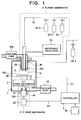
- Fig. 1 shows the construction of a plasma etching apparatus constructed in accordance with a first embodiment of the present invention.
- the plasma etching apparatus as illustrated comprises a treatment chamber in the form of a vacuum vessel 1, a plasma generator 2 installed on the vacuum vessel 1, an X-Y drive mechanism 3 disposed in the vacuum vessel 1, a distance varying means in the form of a Z drive mechanism 4 disposed below the vacuum vessel 1, and a first and a second control means in the form of a controller 5.
- the plasma generator 2 comprises a conduit 20, a plurality of gas cylinders 22-1, 22-2, 22-3 respectively storing gases to be supplied to the conduit 20 through supply pipes 21, and a microwave oscillator 23 mounted on an outer side of the conduit 20.
- the conduit 20 is fixed to an upper portion of the vacuum vessel 1 and has an ejection opening 20a of a predetermined inner diameter D directed toward a stage 30.
- the gas cylinders 22-1, 22-2, 22-3 store a sulfur hexafluoride (SF 6 ) gas, an oxygen (O 2 ) gas, and an argon (Ar) gas, respectively.
- SF 6 sulfur hexafluoride
- O 2 oxygen
- Ar argon
- the microwave oscillator 23 comprises a magnetron and the like, and serves to radiate a microwave of a predetermined power toward a plasma generating area defined inside the conduit 20.
- a mixed gas comprising the SF 6 gas, the O 2 gas, and the Ar gas with a predetermined composition is supplied to the conduit 20, and microwave of the predetermined magnitude or power is radiated by the microwave oscillator 23 toward the plasma generating area in the conduit 20, so that a plasma containing an active species gas in the form of fluorine (F) gas G is created, the F gas being flowing toward a downstream side.
- the conduit 20 ejects the F gas to a surface of an object to be etched in the form of a wafer 110, thereby etching it.
- an exhaust pipe 24 Through the outside of the conduit 20, there is provided an exhaust pipe 24 through which unnecessary etching products created upon F-gas etching are caused to discharge to the outside of the vacuum vessel 1 under the action of a vacuum pump 24a.
- a gas cylinder 22-4 storing therein a hydrogen gas which is to be supplied to the vacuum vessel 1 to make the interior space of the vacuum vessel 1 into a hydrogen atmosphere.
- the X-Y drive mechanism 3 is a well-known mechanism which is capable of moving the stage 30 in an X-axis direction and in a Y-axis direction (i.e., in the right and left direction and in a direction perpendicular to the drawing sheet of Fig. 1) by means of unillustrated servo-motors.
- the Z drive mechanism 4 is also a well-known conveying mechanism for moving the X-Y drive mechanism 3 in a Z-axis direction (i.e., in a vertical direction in Fig. 1) so as to change the distance between the ejection opening 20a of the conduit 20 and the adjacent surface of the wafer 110.
- the Z drive mechanism 4 comprises a linear guide device 40 and an electric motor 42.
- the linear guide device 40 is fixed to a support 41 firmly attached to a lower surface of the vacuum vessel 1, and has a shaft 40a which is coupled at its upper end to the X-Y drive mechanism 3.
- the motor 42 is controlled by the controller 5 and has a rotation shaft 42a coupled to the linear guide device 40.
- the linear guide device 40 coupled to the rotation shaft 42a converts the rotary motion of the rotation shaft 42a into an upward movement of its shaft 40a.
- the shaft 40a the upper end of which is coupled to the X-Y drive mechanism 3, raises the X-Y drive mechanism 3, whereby the stage 30 is moved in an upward direction together with the X-Y drive mechanism 3, casing the wafer 110 to approach the ejection opening 20a.
- reverse rotation of the rotation shaft 42a of the motor 42 causes the stage 30 to fall or lower, thus moving the wafer 110 away from the ejection opening 20a.
- the controller 5 serves to control the X-Y drive mechanism 3 and the Z drive mechanism 4.
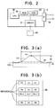
- the controller 5 comprises a CPU 50, a driver 51 connected to the CPU 50 through a bus, a ROM 52 and a RAM 53, and is connected to the X-Y drive mechanism 3 and the Z drive mechanism 4 through an interface 54, which is indicated at a reference symbol IF in Fig. 2.
- the driver 51 is a drive mechanism capable of reproducing data stored in the recording medium 55 such as a floppy disc, a magneto-optical disc, etc.
- the recording medium 55 used for the driver 51 pre-stores data relating to respective convexes existing on the surface of the wafer 110.
- Fig. 3 is a schematic view showing the convex data stored in the recording medium 55. As shown in this figure, let us assume that there are N convexes on the surface of the wafer 110, and that position data representative of the position of each convex and area-and-height data representative of the area and height of each convex are measured and stored in the recording medium 55 beforehand. More specifically, as clearly shown in Fig.
- a position data Pn representative of the position of the nth convex 111 in X-Y coordinates, an area data Ln representative of the diameter of the nearest contour to a reference line B1 indicated at a chain line, and a height data Hn representative of the height of the nth convex 111 in a Z coordinate are recorded or stored as a single piece of record.
- record data for the 1st through Nth convexes 111 are stored in the recording medium 55.
- the CPU 50 has a function of generating an X-Y control signal C1 for controlling the X-Y drive mechanism 3 and a Z control signal C2 for controlling the Z drive mechanism 4 based on the data read out of the recording medium 55 through the RAM 53 and outputting it to the X-Y drive mechanism 3 and the Z drive mechanism 4.
- a control program to be executed by the CPU 50 for performing such a function is stored in the ROM 52, so that the CPU 50 can carry out various control based on the control program.
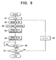
- Fig. 4 is a flow chart showing a control operation of the controller 5.
- the controller 5 controls the X-Y drive mechanism 3 and the Z drive mechanism 4, and sequentially processes the 1st through Nth convexes 111 in this order.
- the CPU 50 reads out the position data Pn from the record for the nth convex 111 (steps S1, S2), and generates an X-Y control signal C1 for controlling the X-Y drive mechanism 3 at a high speed so that the nth convex 111 is moved to a position just under the ejection opening 20a, as shown in Fig. 1 (step S3).
- the area data Ln for the nth convex 111 is read in and It is determined whether the area data Ln is greater than a predetermined reference value L0 (step S4).
- the controller 5 When the area data Ln is greater than the reference value L0, the controller 5 generates a Z control signal C2 for controlling the Z drive mechanism 4 so that the distance between the ejection opening 20a and the reference surface B1 is adjusted to a first predetermined value Z0 ("YES" in step S4, and step S5).
- a Z control signal C2 is generated for controlling the Z drive mechanism 4 such that the distance between the ejection opening 20a and the reference surface B1 is adjusted to a second predetermined value Z0', which is less than the first predetermined value Z0 ("NO" in step S4, and step S11).
- the reference value L0 is a value of the diameter of a diffusion area of the F gas G when the height of the ejection opening 20a from the reference surface B1 is of the first predetermined value Z0, and hence it represents a corresponding etching area.
- the reference value L0' is a value of the diameter of a diffusion area of the F gas G when the height of the ejection opening 20a from the reference surface B1 is equal to the second predetermined value Z0', and hence it represents a corresponding etching area.
- the controller 5 reads in the height data Hn, calculates a stay time Tn substantially in proportion to the height data Hn, and controls such that the nth convex 111 is stayed stationary at a position just under the ejection opening 20a only for the stay time Tn (steps S6, S7). That is, the controller 5 performs substantially the same processing as it controls an ejection time of the F gas G ejected from the election opening 20a in accordance with the size of the convex 111.
- the diameter of the corresponding etching area is equal to the reference value L0.
- the area Ln of the nth convex 111 is greater than the reference value L0, a large part of the peripheral portion of the nth convex 111 might remain intact (non-etched) after the etching treatment.
- step S9 it is determined whether the nth convex 111 is the last one. If the answer to this question is negative, the next position data Pn+1 for the next (n+1)th convex 111 is read in so that the X-Y drive mechanism 3 is fast controlled to swiftly move the next convex 111 to a position just under the ejection opening 20a. Then, the same processing as above is repeated ("NO" in step S9, steps S10, S2 and S3). On the other hand, if the nth convex 111 is the last one, the processing is finished ("YES" in step S9).
- the recording medium 55 storing the above records is set on the driver 51 of the controller 5, as shown in Fig. 2, and the plasma generator 2 and the controller 5 shown in Fig. 1 are actuated so that the F gas G is ejected from the ejection opening 20a of the diameter D toward the silicon wafer 110.
- the CPU 50 reads in the position data P1 from the record for the convex 111-1 (steps S1, S2 in Fig. 4), and generates an X-Y control signal C1 to the X-Y drive mechanism 3.
- the X-Y drive mechanism 3 drives the stage 30 at a high speed to place the convex 111-1 to a position just under the ejection opening 20a (step S3 in Fig. 4).
- an area data L1 for the convex 111-1 is read in, but the area data L1 thus read in is greater than the reference value L0, so that a Z control signal C2 is output from the controller 5 to the Z drive mechanism 4 which drives the X-Y drive mechanism 3 and the stage 30 to move in unison in a downward direction to such an extent that the distance between the ejection opening 20a and the reference surface B1 becomes equal to the first predetermined value Z0 ("YES" in step S4, and step S5 in Fig. 4).
- the convex 111-1 stays at a position just under the ejection opening 20a only for the period of time T1 calculated based on the height data H1 (step S7 in Fig. 4), so that the F gas G is ejected to the convex 111-1 for a longer period of time.
- the etching area for the convex 111-1 is flattened very well.
- an X-Y control signal C1 is generated from the controller 5 to the X-Y drive mechanism 3, whereby the convex 111-1 is swung or moved by a distance (L1-L0)/2 both in the X-axis direction and in the Y-axis direction, thus etching the peripheral portion of the convex 111-1 in a uniform manner (step S8 in Fig. 4), whereupon the F gas G diffuses to the outside of the convex 111-1, giving rise to a possibility that portions other than the convex 111-1 might be etched.
- the atmosphere surrounding the F gas G is filled with a hydrogen gas supplied from the gas cylinder 22-4, so the F gas G having diffused to the outside of the convex 111-1 reacts with the hydrogen gas to be turned into an inactive HF gas. As a result, substantially no etching will take place on the portions of the wafer 110 outside the convex 111-1.
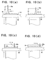
- the next convex 111-2 is selected as a target, and the position data P2 for the convex 111-2 is read in ("NO" in steps S9, S10 and S2 in Fig. 4), whereby the convex 111-2 is moved to a position just under the ejection opening 20a at a high speed (step S3 in Fig. 4), as shown in Fig. 8(b).
- step S3 in Fig. 4 the same processing operation as in the case of the convex 111-1 will be carried out (steps S4 through S9).
- H2 ⁇ H1 the stay time T2 of the convex 111-2 is shorter than the stay time T1 of the convex 111-1.
- the convex 111-3 is selected as the following target, and the position data P3 of the convex 111-3 is read in, so that the convex 111-3 is fast moved to a position just under the ejection opening 20a ("NO" in steps S9, S10, S2, S3 in Fig. 4).
- the area data L3 of the convex 111-3 is read in, which is less than the reference value L0, so that the stage 30 is driven to move in the upward direction to such an extent that the distance between the ejection opening 20a and the reference surface B1 is reduced to the second preset value Z0' ("NO" in steps S4 and S11 in Fig. 4).
- the convex 111-3 is subjected to etching by means of the F gas G which is ejected to and diffused over that etching area.
- the convex 111-3 is stayed stationary just under the ejection opening 20a only for a period of time T3 ( ⁇ T2 ) calculated on the basis of the height data H3 (steps S6 and S7 in Fig 4), and then it is swung or moved by a distance (L3 - L0')/2 both in the X-axis direction and in the Y-axis direction, so that the convex 111-3 is uniformly etched (step S8 in Fig. 4).
- the convex 111-4 is selected as a target, and the position data P4 thereof is read in. As shown in Fig. 8(d), the convex 111-4 is moved to a position just under the ejection opening 20a at a high speed ("NO" in steps S9, S10, S2, and S3). Thereafter, the same processing operation is carried out as in the case of the above-mentioned convex 111-3 (steps S4, and S11 through S8).
- the stay time T4 of the convex 111-4 is the shortest, and since the area data L4 of the convex 111-4 is equal to the reference value L0', there is no swinging movement of the convex 111-4 in the X-axis and Y-axis directions.
- the plasma etching apparatus As described above, a plurality of silicon wafers 110 each having a diameter of 6 inches were processed with the result that the total thickness variation (TTV) thereof was improved from 0.48 ⁇ m by 0.25 ⁇ m on the average, and the standard deviation of variation thereof is equal to or less than 0.03. Thus, it was found that the plasma etching apparatus of the present invention exhibits satisfactory performance as a wafer flattening apparatus.
- TTV total thickness variation
- the stage 30 is driven to move in the downward direction to make the distance between the ejection opening 20a and the convex 111 larger so as to ensure a correspondingly large etching area
- the stage 30 is driven to move in the upward direction to make the distance between the ejection opening 20a and the convex 111 smaller so as to ensure a smaller etching area corresponding to the small convex 111.
- each convex is controlled by the height thereof, so that a period of time of ejecting an F gas G can be ensured corresponding to the convex height.
- a variety of convexes 111 having various sizes or areas can be flattened in a reliable and effective manner.
- a plasma etching apparatus in accordance with a second embodiment of the present invention will next be described below, which is different from the aforementioned plasma etching apparatus in accordance with the first embodiment in that the distance between the ejection opening 20a and a wafer 110 to be processed can be varied in a continuous manner.
- Fig. 9 is a flow chart showing the control operation of the controller 5 of this embodiment.
- the steps S1 through S8 for sequentially processing the 1st through Nth convexes 111 in this order, and the steps S2, S3 of reading in the position data Pn of the nth convex 111 and moving this convex 111 to a position just under the ejection opening 20a are the same as the corresponding steps of the above-mentioned first embodiment.
- step S4 the control operation of this embodiment differs from the first embodiment in that the distance Zn between the ejection opening 20a and the reference surface B1 of the wafer 110 (see Fig. 3(a)) is controlled in accordance with the area data Ln.
- the value Zn is such a value that when the F gas G is ejected from this height, an etching area to be etched by the F gas G has a diameter substantially equal to the area data Ln of the nth convex 111, which is dependent on the proportionality factor k experimentally determined.
- nth convex 111 being in the above-mentioned state is stayed stationary just under the ejection opening 20a only for a period of time Tn substantially proportional to the height data Hn, during which it is subjected to an etching operation.
- processing moves to the following or (n+1)th one 111 ("NO" in steps S5 through S7, steps S8 and S2).
- the respective distances Z1 through Z4 between the reference surface B1 and the ejection opening 20a with the 1st through 4th convexes 111-1 through 111-4, respectively, are continuously varied in accordance with the sizes or areas of these convexes 111-1 through 111-4, so that the F gas G can be ejected to and diffused over all the convexes 111-1 through 111-4.
- a plasma etching apparatus in accordance with a third embodiment of the present invention will now be described below, which is different from the aforementioned plasma etching apparatuses in accordance with the first and second embodiments in that the density of F gas G can be varied in dependence upon the size or area of each convex 111.
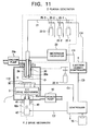
- Fig. 11 illustrates the construction of the plasma etching apparatus of this embodiment
- Fig. 12 is a flow chart showing the control operation of the controller 5 of this embodiment.
- the plasma etching apparatus of this embodiment is equipped with a third control means in the form of an ejection density controller 6 for controlling the operations of electromagnetic valves 25-1 through 25-3 provided on the gas cylinders 22-1 through 22-3 and a microwave oscillator 23.
- a third control means in the form of an ejection density controller 6 for controlling the operations of electromagnetic valves 25-1 through 25-3 provided on the gas cylinders 22-1 through 22-3 and a microwave oscillator 23.
- the steps S1 through S11 for sequentially processing the 1st through Nth convexes 111 in this order, and the steps S3 through S5 and step S12 of reading in the position data Pn of the nth convex 111 and moving this convex 111 to a position just under the ejection opening 20a and controlling the distance Z between the ejection opening 20a and the reference surface B1 based on the area data Ln are the same as the corresponding steps of the above-mentioned first embodiment.
- the control operation of this embodiment differs from the first embodiment in that the ejection density of the F gas G from the conduit 20 is controlled in accordance with the height data Hn of the nth convex 111.
- the value ⁇ n is such a value that when the F gas G of the density ⁇ n is ejected to the nth convex 111, it is possible to flatten the nth convex 111 in a predetermined short period of time T0.
- the value ⁇ n is dependent on the proportionality factor m which is determined experimentally.
- the density control signal C3 indicates an amount of the F gas G comprising SF 6 , O 2 and Ar with a predetermined composition, and an oscillation frequency of the microwave oscillator 23. These values for the F gas amount and the oscillation frequency are beforehand experimentally collected as data.
- the controller 5 outputs the density control signal C3 to the ejection controller 6, and performs, after the lapse of the predetermined time T0, control of swingingly moving the nth convex 111 both in the X-axis and Y-axis directions, after which processing is moved to the following (n+1)th convex 111 (steps S8 through S11, and step S2).
- the ejection density controller 6 shown in Fig. 11 generates a control signal C4 based on the density control signal C3 from the controller 5 to thereby control the electromagnetic valves 25-1 through 25-3, and it also generates a control signal C5 to thereby control the microwave oscillator 23.
- the electromagnetic valves 25-1 through 25-3 are controlled to open and close by the ejection density controller 6, so that the SF 6 gas, the O 2 gas and the Ar gas in the gas cylinders 22-1, 22-2 and 22-3 are supplied to the conduit 20 at respective quantities indicated by the density control signal C3, and the microwave oscillator 23 is controlled to radiate microwave into the conduit 20 at an oscillation frequency indicated by the density control signal C3.
- the ejection density ⁇ 1 of the F gas G for the convex 111-1 is the greatest, and the ejection densities ⁇ 2, ⁇ 3 for the convexes 111-2, 111-3 decrease in this order, with the ejection density ⁇ 4 for the convex 111-4 being the smallest. Accordingly, it is possible to flatten the convexes 111-1 through 111-4 in a predetermined short period of time T0 in a reliable manner, so in comparison with the aforementioned first embodiment in which the stay time of a convex increases in dependence on the size or area thereof, the time required for etching is extremely shortened.
- the stage 30 can be stationary with the conduit 20 of the plasma generator 2 being moved toward or away from the wafer 110.
- the F gas G is continuously ejected from the conduit 20, but during the time when processing is transferred from one convex to the following convex, ejection of the F gas G may be stopped.
- the plasma generating means comprises a plasma generator 2 which radiates microwave of a predetermined power toward the plasma generating area in the conduit 20 to thereby generate a plasma containing an active species gas in the form of an F gas G
- it can comprise, in place of the plasma generator 2, an inductively coupled plasma generator (ICP) using a high-frequency wave, a capacitively coupled plasma generator, a plasma generator using a helicon wave, an electron cyclotron resonance (ECR) source, or the like, for example.
- ICP inductively coupled plasma generator
- ECR electron cyclotron resonance
- the plasma generating gas comprises a mixed gas containing SF 6 , O 2 and Ar, but SF 6 in the mixed gas may be replaced by a fluorocarbon-based gas such as CF 4 .
- height control is effected at two stages or in a stepwise manner in steps S4, S5 and S12 of Fig. 12 as in the first embodiment, it can be carried out in a continuous manner as in the control of the second embodiment (step S4 in Fig. 9).
- the distance adjusting means comprises the Z drive mechanism 4 which is constructed of the linear guide device 40 and the motor 42, but as shown in Fig. 13, it can instead comprise a Z drive mechanism 4' which is constructed of a rotary guide device 40', a motor 42, and a rotation shaft 42a of a gear mechanism 43. That is, the rotational force of the rotation shaft 42a of the motor 42 is received by the rotary guide device 40', and the rotation of the rotation shaft 40a' of the rotary guide device 40' is then converted into a vertical movement by means of the gear mechanism 43.
- a surface flattening treatment on an object to be etched which has convexes having varying sizes or areas simply by changing the distance between a convex to be etched and an ejection opening for ejecting an active species gas in an plasma generating means.
- This serves to shorten the time required for the surface flattening operation.
- Such a surface flattening operation can be carried out by use of the single plasma generating means, so provision of a single treatment chamber is satisfactory for treating or processing a variety of convexes of varying sizes or areas, resulting in a substantial reduction in the cost of equipment.
- a step or process of transporting the object to be etched from one treatment chamber to another treatment chamber can be omitted, thus contributing to an improvement in the total throughput to a substantial extent.
- a period of time of ejecting the active species gas to a convex can be controlled in accordance with the size or area of the convex, so as to flatten the convex having a large area in a reliable manner.
- the ejection time of the active species gas can be shortened so as to flatten the convex having a small area in a reliable and effective manner.
- a density of the active species gas can be controlled in accordance with the area of the convex, so that the time required for the surface flattening operation can further be reduced.
- a hydrogen gas is supplied to surroundings of the active species gas ejected from the ejection opening, so that the active species gas spreading outside the convex reacts with hydrogen, thereby preventing unwanted etching of those portions of the object other than the convex.
Landscapes
- Physics & Mathematics (AREA)
- Engineering & Computer Science (AREA)
- Plasma & Fusion (AREA)
- Chemical & Material Sciences (AREA)
- Analytical Chemistry (AREA)
- Drying Of Semiconductors (AREA)
- ing And Chemical Polishing (AREA)
Applications Claiming Priority (3)
| Application Number | Priority Date | Filing Date | Title |
|---|---|---|---|
| JP32224196A JP3612158B2 (ja) | 1996-11-18 | 1996-11-18 | プラズマエッチング方法及びその装置 |
| JP32224196 | 1996-11-18 | ||
| JP322241/96 | 1996-11-18 |
Publications (2)
| Publication Number | Publication Date |
|---|---|
| EP0843336A2 true EP0843336A2 (de) | 1998-05-20 |
| EP0843336A3 EP0843336A3 (de) | 2000-09-27 |
Family
ID=18141497
Family Applications (1)
| Application Number | Title | Priority Date | Filing Date |
|---|---|---|---|
| EP97119624A Withdrawn EP0843336A3 (de) | 1996-11-18 | 1997-11-10 | Verfahren und Vorrichtung zur Plasmaätzung |
Country Status (3)
| Country | Link |
|---|---|
| US (2) | US5980769A (de) |
| EP (1) | EP0843336A3 (de) |
| JP (1) | JP3612158B2 (de) |
Cited By (5)
| Publication number | Priority date | Publication date | Assignee | Title |
|---|---|---|---|---|
| EP0961314A1 (de) * | 1998-05-28 | 1999-12-01 | Wacker Siltronic Gesellschaft für Halbleitermaterialien Aktiengesellschaft | Hochebene Halbleiterscheibe aus Silicium und Verfahren zur Herstellung von Halbleiterscheiben |
| EP1054443A3 (de) * | 1999-05-12 | 2001-08-29 | Speedfam Co.,Ltd. | Waferätzverfahren |
| EP0989595A3 (de) * | 1998-09-18 | 2001-09-19 | Ims-Ionen Mikrofabrikations Systeme Gmbh | Vorrichtung zur Bearbeitung von Substratoberflächen |
| EP1004401A3 (de) * | 1998-11-26 | 2002-01-23 | Speedfam Co.,Ltd. | Poliervorrichtung für Halbleiter |
| US6451217B1 (en) | 1998-06-09 | 2002-09-17 | Speedfam-Ipec Co., Ltd. | Wafer etching method |
Families Citing this family (42)
| Publication number | Priority date | Publication date | Assignee | Title |
|---|---|---|---|---|
| JPH10242129A (ja) * | 1997-02-26 | 1998-09-11 | Ebara Corp | ガスエッチング方法、ガス噴出用ノズル及びガスエッチング装置 |
| DE19826382C2 (de) * | 1998-06-12 | 2002-02-07 | Bosch Gmbh Robert | Verfahren zum anisotropen Ätzen von Silicium |
| JP2000036488A (ja) * | 1998-07-21 | 2000-02-02 | Speedfam-Ipec Co Ltd | ウエハ平坦化方法及びそのシステム |
| US7780867B1 (en) | 1999-10-01 | 2010-08-24 | Novellus Systems, Inc. | Edge bevel removal of copper from silicon wafers |
| JP2001244240A (ja) | 2000-02-25 | 2001-09-07 | Speedfam Co Ltd | 半導体ウエハの製造方法 |
| US6500356B2 (en) * | 2000-03-27 | 2002-12-31 | Applied Materials, Inc. | Selectively etching silicon using fluorine without plasma |
| US20030010354A1 (en) * | 2000-03-27 | 2003-01-16 | Applied Materials, Inc. | Fluorine process for cleaning semiconductor process chamber |
| US6585572B1 (en) | 2000-08-22 | 2003-07-01 | Lam Research Corporation | Subaperture chemical mechanical polishing system |
| US6640155B2 (en) | 2000-08-22 | 2003-10-28 | Lam Research Corporation | Chemical mechanical polishing apparatus and methods with central control of polishing pressure applied by polishing head |
| US7481695B2 (en) | 2000-08-22 | 2009-01-27 | Lam Research Corporation | Polishing apparatus and methods having high processing workload for controlling polishing pressure applied by polishing head |
| US6652357B1 (en) | 2000-09-22 | 2003-11-25 | Lam Research Corporation | Methods for controlling retaining ring and wafer head tilt for chemical mechanical polishing |
| US6471566B1 (en) | 2000-09-18 | 2002-10-29 | Lam Research Corporation | Sacrificial retaining ring CMP system and methods for implementing the same |
| US6443815B1 (en) | 2000-09-22 | 2002-09-03 | Lam Research Corporation | Apparatus and methods for controlling pad conditioning head tilt for chemical mechanical polishing |
| GB2367788A (en) * | 2000-10-16 | 2002-04-17 | Seiko Epson Corp | Etching using an ink jet print head |
| US6843258B2 (en) * | 2000-12-19 | 2005-01-18 | Applied Materials, Inc. | On-site cleaning gas generation for process chamber cleaning |
| JP2002299321A (ja) * | 2001-03-30 | 2002-10-11 | Speedfam Co Ltd | 局所ドライエッチング装置のためのウェーハテーブル |
| JP2003100717A (ja) | 2001-09-21 | 2003-04-04 | Tokyo Electron Ltd | プラズマ処理装置 |
| US20030121796A1 (en) * | 2001-11-26 | 2003-07-03 | Siegele Stephen H | Generation and distribution of molecular fluorine within a fabrication facility |
| US20040151656A1 (en) * | 2001-11-26 | 2004-08-05 | Siegele Stephen H. | Modular molecular halogen gas generation system |
| US20040037768A1 (en) * | 2001-11-26 | 2004-02-26 | Robert Jackson | Method and system for on-site generation and distribution of a process gas |
| JP2003273082A (ja) * | 2002-03-14 | 2003-09-26 | Tokyo Electron Ltd | プラズマ処理装置及びプラズマ処理方法 |
| US20030221616A1 (en) * | 2002-05-28 | 2003-12-04 | Micron Technology, Inc. | Magnetically-actuatable throttle valve |
| US20040110314A1 (en) * | 2002-12-05 | 2004-06-10 | Ravi Kramadhati V. | Silicon-on-insulator devices and methods for fabricating the same |
| US6979408B2 (en) * | 2002-12-30 | 2005-12-27 | Intel Corporation | Method and apparatus for photomask fabrication |
| JP4134741B2 (ja) * | 2003-01-30 | 2008-08-20 | 松下電器産業株式会社 | プラズマエッチング方法 |
| JP2007149923A (ja) * | 2005-11-28 | 2007-06-14 | Speedfam Co Ltd | 半導体ウェーハの平坦化加工方法 |
| US8100081B1 (en) | 2006-06-30 | 2012-01-24 | Novellus Systems, Inc. | Edge removal of films using externally generated plasma species |
| CN101135333B (zh) * | 2006-08-30 | 2011-01-12 | 北京北方微电子基地设备工艺研究中心有限责任公司 | 连接装置 |
| US9732416B1 (en) | 2007-04-18 | 2017-08-15 | Novellus Systems, Inc. | Wafer chuck with aerodynamic design for turbulence reduction |
| US8419964B2 (en) * | 2008-08-27 | 2013-04-16 | Novellus Systems, Inc. | Apparatus and method for edge bevel removal of copper from silicon wafers |
| EP2224469A3 (de) * | 2009-02-25 | 2015-03-25 | Imec | Verfahren zum Ätzen von 3-D-Strukturen in ein Halbleitersubstrat, einschließlich der Oberflächenbehandlung |
| US8172646B2 (en) * | 2009-02-27 | 2012-05-08 | Novellus Systems, Inc. | Magnetically actuated chuck for edge bevel removal |
| JP6017936B2 (ja) * | 2012-11-27 | 2016-11-02 | 東京エレクトロン株式会社 | プラズマ処理装置およびプラズマ処理方法 |
| FR3011540B1 (fr) * | 2013-10-07 | 2016-01-01 | Centre Nat Rech Scient | Procede et systeme de structuration submicrometrique d'une surface de substrat |
| WO2015137364A1 (ja) * | 2014-03-14 | 2015-09-17 | 独立行政法人産業技術総合研究所 | プラズマ処理装置 |
| US9881788B2 (en) | 2014-05-22 | 2018-01-30 | Lam Research Corporation | Back side deposition apparatus and applications |
| JP6494417B2 (ja) * | 2015-05-20 | 2019-04-03 | 株式会社ディスコ | プラズマエッチング装置 |
| NL2019096B1 (en) * | 2017-06-20 | 2018-12-27 | Suss Microtec Lithography Gmbh | Nozzle tip adapter, nozzle assembly as well as nozzle |
| JP7012602B2 (ja) * | 2018-05-18 | 2022-01-28 | スピードファム株式会社 | 局所ドライエッチング装置 |
| JP6846387B2 (ja) * | 2018-06-22 | 2021-03-24 | 東京エレクトロン株式会社 | プラズマ処理方法及びプラズマ処理装置 |
| CN115244655A (zh) | 2020-01-03 | 2022-10-25 | 朗姆研究公司 | 站与站之间的背面弯曲补偿沉积的控制 |
| JP7645891B2 (ja) | 2020-01-30 | 2025-03-14 | ラム リサーチ コーポレーション | 局所応力調整のためのuv硬化 |
Family Cites Families (17)
| Publication number | Priority date | Publication date | Assignee | Title |
|---|---|---|---|---|
| JPS58157975A (ja) * | 1982-03-10 | 1983-09-20 | Tokyo Ohka Kogyo Co Ltd | プラズマエツチング方法 |
| US4837443A (en) * | 1987-10-15 | 1989-06-06 | The Perkin-Elmer Corporation | Guard ring for a differentially pumped seal apparatus |
| US5082517A (en) * | 1990-08-23 | 1992-01-21 | Texas Instruments Incorporated | Plasma density controller for semiconductor device processing equipment |
| JP2962583B2 (ja) * | 1991-01-28 | 1999-10-12 | 株式会社 ユーハ味覚糖精密工学研究所 | ラジカル反応による無歪精密数値制御加工方法及びその装置 |
| US5254830A (en) * | 1991-05-07 | 1993-10-19 | Hughes Aircraft Company | System for removing material from semiconductor wafers using a contained plasma |
| DE4132565C2 (de) * | 1991-09-30 | 1994-11-10 | Siemens Ag | Verfahren zum isotropen Downstream-Plasmaätzen mit Mikrowellenanregung bei der Herstellung integrierter Halbleiterschaltungen |
| US5290382A (en) * | 1991-12-13 | 1994-03-01 | Hughes Aircraft Company | Methods and apparatus for generating a plasma for "downstream" rapid shaping of surfaces of substrates and films |
| US5336355A (en) * | 1991-12-13 | 1994-08-09 | Hughes Aircraft Company | Methods and apparatus for confinement of a plasma etch region for precision shaping of surfaces of substances and films |
| IL104268A0 (en) * | 1992-01-31 | 1993-05-13 | Hughes Aircraft Co | Reactive gas for plasma assisted chemical etching and methods for stable plasma etching of substrates over edges |
| US5376224A (en) * | 1992-02-27 | 1994-12-27 | Hughes Aircraft Company | Method and apparatus for non-contact plasma polishing and smoothing of uniformly thinned substrates |
| EP0579399A2 (de) * | 1992-07-09 | 1994-01-19 | Pilkington Plc | Glassubstrat für eine Magnetplatte und Herstellungsverfahren dafür |
| US5352324A (en) * | 1992-11-05 | 1994-10-04 | Hitachi, Ltd. | Etching method and etching apparatus therefor |
| US5375064A (en) * | 1993-12-02 | 1994-12-20 | Hughes Aircraft Company | Method and apparatus for moving a material removal tool with low tool accelerations |
| CA2144834C (en) * | 1994-03-17 | 2000-02-08 | Masahiro Miyamoto | Method and apparatus for generating induced plasma |
| US5670018A (en) * | 1995-04-27 | 1997-09-23 | Siemens Aktiengesellschaft | Isotropic silicon etch process that is highly selective to tungsten |
| US5688415A (en) * | 1995-05-30 | 1997-11-18 | Ipec Precision, Inc. | Localized plasma assisted chemical etching through a mask |
| US5879573A (en) * | 1997-08-12 | 1999-03-09 | Vlsi Technology, Inc. | Method for optimizing a gap for plasma processing |
-
1996
- 1996-11-18 JP JP32224196A patent/JP3612158B2/ja not_active Expired - Fee Related
-
1997
- 1997-11-06 US US08/965,281 patent/US5980769A/en not_active Expired - Fee Related
- 1997-11-10 EP EP97119624A patent/EP0843336A3/de not_active Withdrawn
-
1999
- 1999-11-08 US US09/435,575 patent/US6306245B1/en not_active Expired - Fee Related
Cited By (5)
| Publication number | Priority date | Publication date | Assignee | Title |
|---|---|---|---|---|
| EP0961314A1 (de) * | 1998-05-28 | 1999-12-01 | Wacker Siltronic Gesellschaft für Halbleitermaterialien Aktiengesellschaft | Hochebene Halbleiterscheibe aus Silicium und Verfahren zur Herstellung von Halbleiterscheiben |
| US6451217B1 (en) | 1998-06-09 | 2002-09-17 | Speedfam-Ipec Co., Ltd. | Wafer etching method |
| EP0989595A3 (de) * | 1998-09-18 | 2001-09-19 | Ims-Ionen Mikrofabrikations Systeme Gmbh | Vorrichtung zur Bearbeitung von Substratoberflächen |
| EP1004401A3 (de) * | 1998-11-26 | 2002-01-23 | Speedfam Co.,Ltd. | Poliervorrichtung für Halbleiter |
| EP1054443A3 (de) * | 1999-05-12 | 2001-08-29 | Speedfam Co.,Ltd. | Waferätzverfahren |
Also Published As
| Publication number | Publication date |
|---|---|
| US6306245B1 (en) | 2001-10-23 |
| JP3612158B2 (ja) | 2005-01-19 |
| JPH10147893A (ja) | 1998-06-02 |
| EP0843336A3 (de) | 2000-09-27 |
| US5980769A (en) | 1999-11-09 |
Similar Documents
| Publication | Publication Date | Title |
|---|---|---|
| US5980769A (en) | Plasma etching method | |
| JP3487497B2 (ja) | 被処理体収容治具及びこれを用いた熱処理装置 | |
| EP1096554A1 (de) | Einrichtung zur plasma-behandlung | |
| US7179397B2 (en) | Plasma processing methods and apparatus | |
| JP3877082B2 (ja) | 研磨装置及び研磨方法 | |
| US6427621B1 (en) | Plasma processing device and plasma processing method | |
| US6339206B1 (en) | Apparatus and method for adjusting density distribution of a plasma | |
| JP2001244240A (ja) | 半導体ウエハの製造方法 | |
| US20070283887A1 (en) | Microwave Plasma Processing Apparatus | |
| US6360687B1 (en) | Wafer flattening system | |
| US5391260A (en) | Vacuum processing apparatus | |
| US6908566B2 (en) | Local dry etching method | |
| CN114864365B (zh) | 基板制程设备 | |
| KR102898208B1 (ko) | 기판 처리 방법 및 기판 처리 장치 | |
| US20040063329A1 (en) | Multi-step local dry etching method for SOI wafer | |
| JP3908990B2 (ja) | 局所ドライエッチング方法 | |
| JP4460788B2 (ja) | 局所エッチング方法 | |
| CN1620357A (zh) | 计算过度抛光时间和/或最后抛光步骤的抛光时间以控制衬底化学机械式抛光工艺的方法及系统 | |
| JP2002231700A (ja) | ナノトポグラフィ除去方法 | |
| JPH04186619A (ja) | 半導体製造装置 | |
| JP4368615B2 (ja) | 局所ドライエッチング方法 | |
| US20020148812A1 (en) | Method and apparatus for performing plasma process on particles | |
| JP2025116658A (ja) | プラズマ処理装置、およびプラズマ処理方法 | |
| KR100662056B1 (ko) | 웨이퍼의 국부세정장치 및 국부세정방법 | |
| JP2007012663A (ja) | 減圧処理装置及び減圧処理方法 |
Legal Events
| Date | Code | Title | Description |
|---|---|---|---|
| PUAI | Public reference made under article 153(3) epc to a published international application that has entered the european phase |
Free format text: ORIGINAL CODE: 0009012 |
|
| AK | Designated contracting states |
Kind code of ref document: A2 Designated state(s): DE FR GB NL |
|
| AX | Request for extension of the european patent |
Free format text: AL;LT;LV;MK;RO;SI |
|
| PUAL | Search report despatched |
Free format text: ORIGINAL CODE: 0009013 |
|
| AK | Designated contracting states |
Kind code of ref document: A3 Designated state(s): AT BE CH DE DK ES FI FR GB GR IE IT LI LU MC NL PT SE |
|
| AX | Request for extension of the european patent |
Free format text: AL;LT;LV;MK;RO;SI |
|
| 17P | Request for examination filed |
Effective date: 20001010 |
|
| AKX | Designation fees paid |
Free format text: DE FR GB NL |
|
| 17Q | First examination report despatched |
Effective date: 20011130 |
|
| GRAP | Despatch of communication of intention to grant a patent |
Free format text: ORIGINAL CODE: EPIDOSNIGR1 |
|
| STAA | Information on the status of an ep patent application or granted ep patent |
Free format text: STATUS: THE APPLICATION IS DEEMED TO BE WITHDRAWN |
|
| 18D | Application deemed to be withdrawn |
Effective date: 20050531 |