EP0844646A2 - Support pour substrat en forme de disque - Google Patents
Support pour substrat en forme de disque Download PDFInfo
- Publication number
- EP0844646A2 EP0844646A2 EP97890228A EP97890228A EP0844646A2 EP 0844646 A2 EP0844646 A2 EP 0844646A2 EP 97890228 A EP97890228 A EP 97890228A EP 97890228 A EP97890228 A EP 97890228A EP 0844646 A2 EP0844646 A2 EP 0844646A2
- Authority
- EP
- European Patent Office
- Prior art keywords
- carrier
- disc
- shaped object
- shaped
- facing
- Prior art date
- Legal status (The legal status is an assumption and is not a legal conclusion. Google has not performed a legal analysis and makes no representation as to the accuracy of the status listed.)
- Granted
Links
Images

Classifications
-
- H—ELECTRICITY
- H10—SEMICONDUCTOR DEVICES; ELECTRIC SOLID-STATE DEVICES NOT OTHERWISE PROVIDED FOR
- H10P—GENERIC PROCESSES OR APPARATUS FOR THE MANUFACTURE OR TREATMENT OF DEVICES COVERED BY CLASS H10
- H10P72/00—Handling or holding of wafers, substrates or devices during manufacture or treatment thereof
- H10P72/70—Handling or holding of wafers, substrates or devices during manufacture or treatment thereof for supporting or gripping
- H10P72/76—Handling or holding of wafers, substrates or devices during manufacture or treatment thereof for supporting or gripping using mechanical means, e.g. clamps or pinches
- H10P72/7604—Handling or holding of wafers, substrates or devices during manufacture or treatment thereof for supporting or gripping using mechanical means, e.g. clamps or pinches the wafers being placed on a susceptor, stage or support
- H10P72/7611—Handling or holding of wafers, substrates or devices during manufacture or treatment thereof for supporting or gripping using mechanical means, e.g. clamps or pinches the wafers being placed on a susceptor, stage or support characterised by edge profile or support profile
-
- Y—GENERAL TAGGING OF NEW TECHNOLOGICAL DEVELOPMENTS; GENERAL TAGGING OF CROSS-SECTIONAL TECHNOLOGIES SPANNING OVER SEVERAL SECTIONS OF THE IPC; TECHNICAL SUBJECTS COVERED BY FORMER USPC CROSS-REFERENCE ART COLLECTIONS [XRACs] AND DIGESTS
- Y10—TECHNICAL SUBJECTS COVERED BY FORMER USPC
- Y10S—TECHNICAL SUBJECTS COVERED BY FORMER USPC CROSS-REFERENCE ART COLLECTIONS [XRACs] AND DIGESTS
- Y10S134/00—Cleaning and liquid contact with solids
- Y10S134/902—Semiconductor wafer
Definitions
- the invention relates to a carrier for disc-shaped objects, especially for silicon wafers during treatment, in particular etching the same, with the features of the introductory part of claim 1.
- Such carriers are in different embodiments known. There are basically two embodiments, namely Carrier on the surface facing the object to be held Bear cones, which the disc-shaped object to the side hold on (see US 4 903 717 A and US 5 513 668 A) and carriers which the disc-shaped object on the carrier by applying negative pressure hold on (see US 5 421 595 A).
- the known carriers allow the treatment of disc-shaped objects on its surface facing away from the carrier, the surface facing the carrier facing surface is not treated as the treatment medium (e.g. the etching liquid) through the emerging from the ring nozzle between the disc-shaped object and the one facing it Surface of the carrier gas flowing radially outward (primarily Nitrogen) is prevented from approaching the underside of the carrier reach.
- the treatment medium e.g. the etching liquid
- the invention is therefore based on the object of a carrier To make available that not only allows that of the wearer opposite side of the disc-shaped object, but also the Outer edge and an annular edge area facing the wearer Side of the disc-shaped object with a treatment medium to treat.
- this task is carried out at the beginning by a carrier mentioned genre essentially by the characteristics of the characteristic Part of claim 1 solved.
- treatment medium treatment liquid, Etching liquid, rinsing liquid
- treatment medium treatment liquid, Etching liquid, rinsing liquid
- the treatment medium is caused by the gas flow from the Ring nozzle emerges and flows between the object and the carrier, advantageously prevented from doing so than desired to walk towards the center of the disc-shaped object.
- a carrier 1 shown in FIG. 1 is in principle from US 4 903 717 A and US 5 513 668 A known.
- this known carrier 1 is the surface of the disk-shaped object 2 facing from a circular surface 3 of an inner part 4 and an annular surface 5 of an outer (annular) part 6 is formed.
- the outer part 6 are several radially adjustable pins 7 ("pins") arranged by which the object 2 (e.g. a silicon wafer) supports laterally becomes.
- annular nozzle 8 acts as an annular gap between the Parts 4 and 6 is formed.
- the annular nozzle 8 is with Pressurized gas, mainly nitrogen, is applied, so that the disc-shaped Item 2 on the carrier 1, according to the Bernoulli principle is held, in the state of equilibrium as it were over areas 3 and 5 "float".
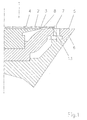
- Fig. 2 it is shown that the edge 11 of the step 10 is rounded, whereas the transition 12 between the outwardly facing surface 13 the level 10 and the radially outside of level 10 part of the the disc-shaped object 2 facing surface 5 of the outer Part 6 sharp edged, or designed with a very small radius of curvature can be.
- the radius of curvature of the step 10 shown in cross section in FIG. 2 decreases radially in a preferred embodiment of the invention outside gradually. So the radius of curvature in the range between A and B, for example 3 mm, in the area between B and C. for example 0.8 mm and in the range between C and D for example 0.2 mm.
- the level 10 results in those indicated schematically in FIG. 3 Flow conditions of the treatment medium 15.
- treatment medium 15 e.g. an etching liquid
- the treatment medium 15 migrates around the peripheral edge 16 of the disc-shaped object 2 around on its underside 17 to approximately in the range of level 10. So an annular Area of the underside 17 of the disk-shaped facing the carrier 1 Item 2 wetted and treated by the treatment medium 15.
- the gas stream emerging from the ring nozzle 8 prevents the treatment medium 15 on the underside of item 2 further migrates inside because the flow of gas from the ring nozzle 8 in one radially within step 10 an inward creep of treatment medium 15 counteracts.
- the stage 10 provided according to the invention can, as shown in FIG. 3, can also be provided for carriers in which the disc-shaped Item 2 is not held laterally by pins, but held on, for example, annular projections of the carrier becomes.
- a carrier is, for example, from US Pat. No. 5,492,566 A known.
- a circular step 10 is provided for the annular nozzle 8.
Landscapes
- Container, Conveyance, Adherence, Positioning, Of Wafer (AREA)
- Weting (AREA)
- ing And Chemical Polishing (AREA)
- Mechanical Treatment Of Semiconductor (AREA)
- Packaging Frangible Articles (AREA)
- Packaging For Recording Disks (AREA)
Priority Applications (1)
| Application Number | Priority Date | Filing Date | Title |
|---|---|---|---|
| AT97890228T ATE276585T1 (de) | 1996-11-20 | 1997-11-14 | Träger für scheibenförmige gegenstände |
Applications Claiming Priority (3)
| Application Number | Priority Date | Filing Date | Title |
|---|---|---|---|
| AT0202496A AT407312B (de) | 1996-11-20 | 1996-11-20 | Rotierbarer träger für kreisrunde, scheibenförmige gegenstände, insbesondere halbleiterwafer oder -substrate |
| AT2024/96 | 1996-11-20 | ||
| AT202496 | 1996-11-20 |
Publications (3)
| Publication Number | Publication Date |
|---|---|
| EP0844646A2 true EP0844646A2 (fr) | 1998-05-27 |
| EP0844646A3 EP0844646A3 (fr) | 1998-08-05 |
| EP0844646B1 EP0844646B1 (fr) | 2004-09-15 |
Family
ID=3526166
Family Applications (1)
| Application Number | Title | Priority Date | Filing Date |
|---|---|---|---|
| EP97890228A Expired - Lifetime EP0844646B1 (fr) | 1996-11-20 | 1997-11-14 | Support pour de substrats en forme de disque |
Country Status (7)
| Country | Link |
|---|---|
| US (1) | US5896877A (fr) |
| EP (1) | EP0844646B1 (fr) |
| JP (1) | JP3995322B2 (fr) |
| KR (1) | KR100499833B1 (fr) |
| AT (2) | AT407312B (fr) |
| DE (1) | DE59711912D1 (fr) |
| TW (1) | TW451387B (fr) |
Cited By (3)
| Publication number | Priority date | Publication date | Assignee | Title |
|---|---|---|---|---|
| EP1372186A3 (fr) * | 2000-10-31 | 2005-10-26 | Sez Ag | Dispositif de traitement de plaquettes |
| DE102008037364A1 (de) | 2008-08-12 | 2010-03-04 | Suss Microtec Lithography Gmbh | Vorrichtung zur Behandlung der Oberfläche eines Substrats durch Auftragen und Abschleudern einer Behandlungsflüssigkeit |
| DE102008062343A1 (de) * | 2008-12-15 | 2010-06-17 | Festo Ag & Co. Kg | Nach dem Bernoulli-Prinzip arbeitender Sauggreifer |
Families Citing this family (38)
| Publication number | Priority date | Publication date | Assignee | Title |
|---|---|---|---|---|
| US6413436B1 (en) * | 1999-01-27 | 2002-07-02 | Semitool, Inc. | Selective treatment of the surface of a microelectronic workpiece |
| US20050217707A1 (en) * | 1998-03-13 | 2005-10-06 | Aegerter Brian K | Selective processing of microelectronic workpiece surfaces |
| US20050020001A1 (en) * | 1998-03-13 | 2005-01-27 | Brian Aegerter | Selective treatment of the surface of a microelectronic workpiece |
| DE19854743A1 (de) * | 1998-11-27 | 2000-06-08 | Sez Semiconduct Equip Zubehoer | Vorrichtung zum Naßätzen einer Kante einer Halbleiterscheibe |
| DE19901291C2 (de) * | 1999-01-15 | 2002-04-18 | Sez Semiconduct Equip Zubehoer | Vorrichtung zur Ätzbehandlung eines scheibenförmigen Gegenstandes |
| DE59900743D1 (de) * | 1999-04-28 | 2002-02-28 | Sez Semiconduct Equip Zubehoer | Vorrichtung und Verfahren zur Flüssigkeitsbehandlung von scheibenförmigen Gegenständen |
| US6203661B1 (en) * | 1999-12-07 | 2001-03-20 | Trusi Technologies, Llc | Brim and gas escape for non-contact wafer holder |
| US6398823B1 (en) | 1999-12-07 | 2002-06-04 | Tru-Si Technologies, Inc. | Dynamic break for non-contact wafer holder |
| TW507312B (en) * | 2000-02-04 | 2002-10-21 | Philips Electron Optics Bv | Particle-optical apparatus, and object carrier therefor |
| SG118063A1 (en) * | 2000-02-11 | 2006-01-27 | Sez Ag | A device for an etch treatment of a disk-like object |
| US6669808B2 (en) | 2001-03-22 | 2003-12-30 | Dainippon Screen Mfg. Co., Ltd. | Substrate processing apparatus and substrate processing method |
| KR100938325B1 (ko) * | 2001-06-13 | 2010-01-22 | 오르보테크 엘티디. | 에너지 전달 시스템 |
| DE10134988C2 (de) * | 2001-07-18 | 2003-08-07 | Infineon Technologies Ag | Aufnahmeteller für einen Wafer und Wafer-Hebevorrichtung |
| US6689418B2 (en) | 2001-08-03 | 2004-02-10 | Applied Materials Inc. | Apparatus for wafer rinse and clean and edge etching |
| US6786996B2 (en) | 2001-10-16 | 2004-09-07 | Applied Materials Inc. | Apparatus and method for edge bead removal |
| US6708701B2 (en) | 2001-10-16 | 2004-03-23 | Applied Materials Inc. | Capillary ring |
| JP4018958B2 (ja) | 2001-10-30 | 2007-12-05 | 大日本スクリーン製造株式会社 | 基板処理装置 |
| AT411335B (de) * | 2002-03-06 | 2003-12-29 | Sez Ag | Verfahren zum nassbehandeln von scheibenförmigen gegenständen |
| US6908567B2 (en) * | 2002-07-30 | 2005-06-21 | Applied Materials Israel, Ltd. | Contaminant removal by laser-accelerated fluid |
| DE10247051A1 (de) * | 2002-10-09 | 2004-04-22 | Polymer Latex Gmbh & Co Kg | Latex und Verfahren zu seiner Herstellung |
| US7001827B2 (en) * | 2003-04-15 | 2006-02-21 | International Business Machines Corporation | Semiconductor wafer front side protection |
| US20040206304A1 (en) * | 2003-04-15 | 2004-10-21 | Menear John Edgar | Pressurized chuck for controlling backside wafer contamination |
| US7100954B2 (en) * | 2003-07-11 | 2006-09-05 | Nexx Systems, Inc. | Ultra-thin wafer handling system |
| JP4312001B2 (ja) * | 2003-07-28 | 2009-08-12 | リアライズ・アドバンストテクノロジ株式会社 | 基板支持装置および基板取り外し方法 |
| DE20318462U1 (de) * | 2003-11-26 | 2004-03-11 | Infineon Technologies Ag | Anordnung elektronischer Halbleiterbauelemente auf einem Trägersystem zur Behandlung der Halbleiterbauelemente mit einem flüssigen Medium |
| US20060040111A1 (en) * | 2004-08-20 | 2006-02-23 | Dolechek Kert L | Process chamber and system for thinning a semiconductor workpiece |
| US7193295B2 (en) * | 2004-08-20 | 2007-03-20 | Semitool, Inc. | Process and apparatus for thinning a semiconductor workpiece |
| US20060046499A1 (en) * | 2004-08-20 | 2006-03-02 | Dolechek Kert L | Apparatus for use in thinning a semiconductor workpiece |
| US7354649B2 (en) | 2004-08-20 | 2008-04-08 | Semitool, Inc. | Semiconductor workpiece |
| US7288489B2 (en) * | 2004-08-20 | 2007-10-30 | Semitool, Inc. | Process for thinning a semiconductor workpiece |
| JP5013400B2 (ja) * | 2006-09-29 | 2012-08-29 | 国立大学法人東北大学 | 塗布膜コーティング装置 |
| JP4954795B2 (ja) * | 2007-05-31 | 2012-06-20 | 芝浦メカトロニクス株式会社 | 基板の保持装置及び基板の処理方法 |
| JP5341939B2 (ja) * | 2011-03-31 | 2013-11-13 | 大日本スクリーン製造株式会社 | 基板周縁処理装置および基板周縁処理方法 |
| JP5513432B2 (ja) * | 2011-03-31 | 2014-06-04 | 大日本スクリーン製造株式会社 | 基板周縁処理装置及び基板周縁処理方法 |
| US10707099B2 (en) | 2013-08-12 | 2020-07-07 | Veeco Instruments Inc. | Collection chamber apparatus to separate multiple fluids during the semiconductor wafer processing cycle |
| JP6158737B2 (ja) * | 2014-03-31 | 2017-07-05 | 芝浦メカトロニクス株式会社 | 基板処理装置及び基板処理方法 |
| US11342215B2 (en) | 2017-04-25 | 2022-05-24 | Veeco Instruments Inc. | Semiconductor wafer processing chamber |
| JP7738507B2 (ja) * | 2022-03-24 | 2025-09-12 | 株式会社Screenホールディングス | 基板処理装置 |
Family Cites Families (7)
| Publication number | Priority date | Publication date | Assignee | Title |
|---|---|---|---|---|
| US4603466A (en) * | 1984-02-17 | 1986-08-05 | Gca Corporation | Wafer chuck |
| AT389959B (de) * | 1987-11-09 | 1990-02-26 | Sez Semiconduct Equip Zubehoer | Vorrichtung zum aetzen von scheibenfoermigen gegenstaenden, insbesondere von siliziumscheiben |
| US5447570A (en) * | 1990-04-23 | 1995-09-05 | Genus, Inc. | Purge gas in wafer coating area selection |
| JP2981795B2 (ja) * | 1991-10-24 | 1999-11-22 | 東京エレクトロン株式会社 | 静電チャック |
| ATE174155T1 (de) * | 1993-02-08 | 1998-12-15 | Sez Semiconduct Equip Zubehoer | Träger für scheibenförmige gegenstände |
| AT639U1 (de) * | 1993-02-08 | 1996-02-26 | Sez Semiconduct Equip Zubehoer | Träger nach dem bernoulli-prinzip für scheibenförmige gegenstände, insbesondere siliziumscheiben |
| EP0611273B1 (fr) * | 1993-02-08 | 1998-09-16 | SEZ Semiconductor-Equipment Zubehör für die Halbleiterfertigung AG | Support pour objets en forme de disque |
-
1996
- 1996-11-20 AT AT0202496A patent/AT407312B/de not_active IP Right Cessation
-
1997
- 1997-11-13 JP JP31242097A patent/JP3995322B2/ja not_active Expired - Lifetime
- 1997-11-14 AT AT97890228T patent/ATE276585T1/de active
- 1997-11-14 DE DE59711912T patent/DE59711912D1/de not_active Expired - Lifetime
- 1997-11-14 EP EP97890228A patent/EP0844646B1/fr not_active Expired - Lifetime
- 1997-11-17 KR KR1019970060329A patent/KR100499833B1/ko not_active Expired - Lifetime
- 1997-11-17 US US08/971,754 patent/US5896877A/en not_active Expired - Lifetime
- 1997-12-02 TW TW086118087A patent/TW451387B/zh active
Cited By (10)
| Publication number | Priority date | Publication date | Assignee | Title |
|---|---|---|---|---|
| EP1372186A3 (fr) * | 2000-10-31 | 2005-10-26 | Sez Ag | Dispositif de traitement de plaquettes |
| EP1369904A3 (fr) * | 2000-10-31 | 2005-10-26 | Sez Ag | Dispositif de traitement de plaquettes |
| US7172674B2 (en) | 2000-10-31 | 2007-02-06 | Sez Ag | Device for liquid treatment of wafer-shaped articles |
| KR100789337B1 (ko) * | 2000-10-31 | 2007-12-28 | 세즈 아게 | 웨이퍼 형상 물품의 액체 처리 장치 |
| KR100796709B1 (ko) * | 2000-10-31 | 2008-01-21 | 세즈 아게 | 웨이퍼 형상 물품의 액체 처리 장치 |
| US7799695B2 (en) | 2000-10-31 | 2010-09-21 | Lam Research Ag | Device for liquid treatment of wafer-shaped articles |
| US7988818B2 (en) | 2000-10-31 | 2011-08-02 | Lam Research Ag | Device for liquid treatment of wafer-shaped articles |
| DE102008037364A1 (de) | 2008-08-12 | 2010-03-04 | Suss Microtec Lithography Gmbh | Vorrichtung zur Behandlung der Oberfläche eines Substrats durch Auftragen und Abschleudern einer Behandlungsflüssigkeit |
| DE102008062343A1 (de) * | 2008-12-15 | 2010-06-17 | Festo Ag & Co. Kg | Nach dem Bernoulli-Prinzip arbeitender Sauggreifer |
| DE102008062343B4 (de) * | 2008-12-15 | 2013-05-29 | Festo Ag & Co. Kg | Nach dem Bernoulli-Prinzip arbeitender Sauggreifer |
Also Published As
| Publication number | Publication date |
|---|---|
| KR19980042486A (ko) | 1998-08-17 |
| KR100499833B1 (ko) | 2005-09-08 |
| EP0844646A3 (fr) | 1998-08-05 |
| JP3995322B2 (ja) | 2007-10-24 |
| TW451387B (en) | 2001-08-21 |
| DE59711912D1 (de) | 2004-10-21 |
| ATA202496A (de) | 2000-06-15 |
| JPH10237678A (ja) | 1998-09-08 |
| US5896877A (en) | 1999-04-27 |
| ATE276585T1 (de) | 2004-10-15 |
| EP0844646B1 (fr) | 2004-09-15 |
| AT407312B (de) | 2001-02-26 |
Similar Documents
| Publication | Publication Date | Title |
|---|---|---|
| EP0844646A2 (fr) | Support pour substrat en forme de disque | |
| EP1020894B1 (fr) | Dispositif d'attaque chimique d'un objet en forme de disque | |
| EP0611273B1 (fr) | Support pour objets en forme de disque | |
| DE3439371C2 (fr) | ||
| DE19983651B4 (de) | Fluidsteuerung | |
| DE3431795C2 (fr) | ||
| EP1170107B1 (fr) | Outil de coupe sous forme de disque | |
| EP1170782A2 (fr) | Dispositif pour manipuler un objet en forme de disque | |
| DE202019104789U1 (de) | Vorrichtung zur Halterung einer Mehrzahl von Trinkhalmen aus Glas, Kunststoff, Metall | |
| DE3244233A1 (de) | Reissfaehige druckentlastungsvorrichtung | |
| DE69508882T2 (de) | Struktur zum Abdichten des Innenumfangs einer Metallmembran | |
| DE4318676A1 (de) | Verfahren zur Verringerung einer teilchenförmigen Konzentration in Arbeitsfluiden | |
| DE69619777T2 (de) | Dichtungseinheit für Gasspülung | |
| DE2742194C3 (de) | Filtriergerät für Genußmittel, insbesondere Kaffee | |
| DE2654917A1 (de) | Expansionsventil | |
| DE69902035T2 (de) | Verfahren zum zusammenkleben von trägern für optische platten | |
| DE4116392C2 (de) | Halterung zur einseitigen Naßätzung von Halbleiterscheiben | |
| EP0965407A1 (fr) | Outil pour travailler des matériaux durs | |
| DE3827072A1 (de) | Kuenstliche augenlinse | |
| DE9311251U1 (de) | Vorrichtung zum Zentrifugieren eines Blutbeutelsystems | |
| AT639U1 (de) | Träger nach dem bernoulli-prinzip für scheibenförmige gegenstände, insbesondere siliziumscheiben | |
| AT1416U1 (de) | Vorrichtung zur abdeckung von pflanzgefässen | |
| DE19804976C1 (de) | Substratscheibe | |
| DE3128248C2 (fr) | ||
| DE3000805C2 (de) | Von außen gehaltener zylindrischer Breithalter für Schlauchware |
Legal Events
| Date | Code | Title | Description |
|---|---|---|---|
| PUAI | Public reference made under article 153(3) epc to a published international application that has entered the european phase |
Free format text: ORIGINAL CODE: 0009012 |
|
| AK | Designated contracting states |
Kind code of ref document: A2 Designated state(s): AT CH DE FR GB IT LI |
|
| PUAL | Search report despatched |
Free format text: ORIGINAL CODE: 0009013 |
|
| AK | Designated contracting states |
Kind code of ref document: A3 Designated state(s): AT BE CH DE DK ES FI FR GB GR IE IT LI LU MC NL PT SE |
|
| 17P | Request for examination filed |
Effective date: 19980808 |
|
| AKX | Designation fees paid |
Free format text: AT CH DE FR GB IT LI |
|
| RBV | Designated contracting states (corrected) |
Designated state(s): AT CH DE FR GB IT LI |
|
| RAP1 | Party data changed (applicant data changed or rights of an application transferred) |
Owner name: SEZ AG |
|
| 17Q | First examination report despatched |
Effective date: 20030416 |
|
| GRAP | Despatch of communication of intention to grant a patent |
Free format text: ORIGINAL CODE: EPIDOSNIGR1 |
|
| GRAS | Grant fee paid |
Free format text: ORIGINAL CODE: EPIDOSNIGR3 |
|
| GRAA | (expected) grant |
Free format text: ORIGINAL CODE: 0009210 |
|
| AK | Designated contracting states |
Kind code of ref document: B1 Designated state(s): AT CH DE FR GB IT LI |
|
| REG | Reference to a national code |
Ref country code: GB Ref legal event code: FG4D Free format text: NOT ENGLISH Ref country code: CH Ref legal event code: EP |
|
| GBT | Gb: translation of ep patent filed (gb section 77(6)(a)/1977) |
Effective date: 20040915 |
|
| REF | Corresponds to: |
Ref document number: 59711912 Country of ref document: DE Date of ref document: 20041021 Kind code of ref document: P |
|
| PG25 | Lapsed in a contracting state [announced via postgrant information from national office to epo] |
Ref country code: LI Free format text: LAPSE BECAUSE OF NON-PAYMENT OF DUE FEES Effective date: 20041130 Ref country code: CH Free format text: LAPSE BECAUSE OF NON-PAYMENT OF DUE FEES Effective date: 20041130 |
|
| ET | Fr: translation filed | ||
| REG | Reference to a national code |
Ref country code: CH Ref legal event code: PL |
|
| PLBE | No opposition filed within time limit |
Free format text: ORIGINAL CODE: 0009261 |
|
| STAA | Information on the status of an ep patent application or granted ep patent |
Free format text: STATUS: NO OPPOSITION FILED WITHIN TIME LIMIT |
|
| 26N | No opposition filed |
Effective date: 20050616 |
|
| REG | Reference to a national code |
Ref country code: FR Ref legal event code: CA |
|
| REG | Reference to a national code |
Ref country code: FR Ref legal event code: CD Ref country code: FR Ref legal event code: CA |
|
| PGFP | Annual fee paid to national office [announced via postgrant information from national office to epo] |
Ref country code: GB Payment date: 20101118 Year of fee payment: 14 Ref country code: IT Payment date: 20101122 Year of fee payment: 14 |
|
| GBPC | Gb: european patent ceased through non-payment of renewal fee |
Effective date: 20111114 |
|
| PG25 | Lapsed in a contracting state [announced via postgrant information from national office to epo] |
Ref country code: IT Free format text: LAPSE BECAUSE OF NON-PAYMENT OF DUE FEES Effective date: 20111114 |
|
| PG25 | Lapsed in a contracting state [announced via postgrant information from national office to epo] |
Ref country code: GB Free format text: LAPSE BECAUSE OF NON-PAYMENT OF DUE FEES Effective date: 20111114 |
|
| PGFP | Annual fee paid to national office [announced via postgrant information from national office to epo] |
Ref country code: FR Payment date: 20121130 Year of fee payment: 16 |
|
| PGFP | Annual fee paid to national office [announced via postgrant information from national office to epo] |
Ref country code: DE Payment date: 20131121 Year of fee payment: 17 Ref country code: AT Payment date: 20131113 Year of fee payment: 17 |
|
| REG | Reference to a national code |
Ref country code: FR Ref legal event code: ST Effective date: 20140731 |
|
| PG25 | Lapsed in a contracting state [announced via postgrant information from national office to epo] |
Ref country code: FR Free format text: LAPSE BECAUSE OF NON-PAYMENT OF DUE FEES Effective date: 20131202 |
|
| REG | Reference to a national code |
Ref country code: DE Ref legal event code: R119 Ref document number: 59711912 Country of ref document: DE |
|
| REG | Reference to a national code |
Ref country code: AT Ref legal event code: MM01 Ref document number: 276585 Country of ref document: AT Kind code of ref document: T Effective date: 20141114 |
|
| PG25 | Lapsed in a contracting state [announced via postgrant information from national office to epo] |
Ref country code: AT Free format text: LAPSE BECAUSE OF NON-PAYMENT OF DUE FEES Effective date: 20141114 |
|
| PG25 | Lapsed in a contracting state [announced via postgrant information from national office to epo] |
Ref country code: DE Free format text: LAPSE BECAUSE OF NON-PAYMENT OF DUE FEES Effective date: 20150602 |