EP0844650A2 - Verfahren zum Aetzen von Sio2 und Verfahren zur Reinigung von Siliziumscheiben unter Verwendung von verdünnten Aetzmitteln und Megaschall - Google Patents
Verfahren zum Aetzen von Sio2 und Verfahren zur Reinigung von Siliziumscheiben unter Verwendung von verdünnten Aetzmitteln und Megaschall Download PDFInfo
- Publication number
- EP0844650A2 EP0844650A2 EP97307698A EP97307698A EP0844650A2 EP 0844650 A2 EP0844650 A2 EP 0844650A2 EP 97307698 A EP97307698 A EP 97307698A EP 97307698 A EP97307698 A EP 97307698A EP 0844650 A2 EP0844650 A2 EP 0844650A2
- Authority
- EP
- European Patent Office
- Prior art keywords
- silicon
- etchant
- dioxide layer
- silicon dioxide
- etching
- Prior art date
- Legal status (The legal status is an assumption and is not a legal conclusion. Google has not performed a legal analysis and makes no representation as to the accuracy of the status listed.)
- Withdrawn
Links
Images


Classifications
-
- H—ELECTRICITY
- H10—SEMICONDUCTOR DEVICES; ELECTRIC SOLID-STATE DEVICES NOT OTHERWISE PROVIDED FOR
- H10P—GENERIC PROCESSES OR APPARATUS FOR THE MANUFACTURE OR TREATMENT OF DEVICES COVERED BY CLASS H10
- H10P70/00—Cleaning of wafers, substrates or parts of devices
- H10P70/10—Cleaning before device manufacture, i.e. Begin-Of-Line process
- H10P70/15—Cleaning before device manufacture, i.e. Begin-Of-Line process by wet cleaning only
-
- H—ELECTRICITY
- H10—SEMICONDUCTOR DEVICES; ELECTRIC SOLID-STATE DEVICES NOT OTHERWISE PROVIDED FOR
- H10P—GENERIC PROCESSES OR APPARATUS FOR THE MANUFACTURE OR TREATMENT OF DEVICES COVERED BY CLASS H10
- H10P50/00—Etching of wafers, substrates or parts of devices
- H10P50/20—Dry etching; Plasma etching; Reactive-ion etching
- H10P50/28—Dry etching; Plasma etching; Reactive-ion etching of insulating materials
- H10P50/282—Dry etching; Plasma etching; Reactive-ion etching of insulating materials of inorganic materials
- H10P50/283—Dry etching; Plasma etching; Reactive-ion etching of insulating materials of inorganic materials by chemical means
Definitions
- the present invention generally relates to the production of silicon bodies, and specifically, to a process for controllably etching silicon dioxide from the surface of such bodies.
- the invention particularly relates, in a preferred embodiment, to a process for cleaning the surface of single crystal silicon bodies, such as wafers.
- Microelectronic semiconductor devices are typically fabricated on single crystal silicon wafers produced from single crystal ingots commercially grown by the well-known Czochralski method.
- the silicon wafers are typically prepared through a sequence of steps in which the ingot is trimmed to a precise diameter, flattened along one or more sides to identify crystallographic orientation, etched to remove mechanical defects, and then sliced along a specific orientation into unfinished wafers.
- the unfinished wafers are precisely shaped through further fabrication steps including edge-rounding, lapping, etching and polishing.
- RCA method is a well known commercial method for cleaning silicon wafers.
- the wafer is sequentially exposed to two different chemical solutions, typically referred to as “Standard Cleaning 1” (SC1) and “Standard Cleaning 2” (SC2) solutions.
- SC1 Standard Cleaning 1
- SC2 Standard Cleaning 2
- the SC1 solution consists of ammonium hydroxide, hydrogen peroxide and water in respective ratios ranging from about 1:2:7 to about 1:1:5 parts by volume of commercially available reagents, typically supplied as 28-30 wt% NH 4 OH in water and as 30-35 wt% H 2 O 2 in water.
- the ratios of ammonium hydroxide and hydrogen peroxide are expressed relative to water, but independent of each other.
- the ratio of NH 4 OH:H 2 O ranges from about 1:7 to about 1:5, the ratio of H 2 O 2 :H 2 O ranges from about 2:7 to about 1:5, and both of these ratios (NH 4 OH:H 2 O and H 2 O 2 :H 2 O) are independent of each other.
- concentration of NH 4 OH in SCl typically ranges from about 35,000 ppm to 50,000 ppm.
- SC1 solutions with ratios of reagents of about 1:4:20 NH 4 OH:H 2 O 2 :H 2 O (approximately 13,300 ppm NH 4 OH) or of about 1:20:100 (approximately 2,800 ppm NH 4 OH) are also known in the art. Meuris et al., A New Cleaning Concept for Particle and Metal Removal on Si Surfaces, Electrochem. Soc. Proc. Vol. 94-7, pp. 15-24 (1994).
- the ammonium hydroxide and hydrogen peroxide in the SC1 solution simultaneously etch the silicon dioxide layer and oxidize the underlying silicon substrate,respectively. As it etches, the ammonium hydroxide removes organic contaminants and also complexes metallic contaminants such as copper, gold, nickel, cobalt and cadmium. However, an alkaline etchant, such as NH 4 OH, would, if it came in contact with the underlying silicon substrate, etch the silicon in an anisotropic, crystal-orientation dependent manner and severely roughen the surface.
- the hydrogen peroxide in the SC1 solution prevents the ammonium hydroxide from etching the underlying silicon substrate.
- the rate of etching SiO 2 in the SC1 cleaning system is typically about 1-5 ⁇ /min. However, etch rates of conventional SC1 solutions vary considerably with time, leading to non-uniform cleaning of silicon bodies. Additionally, the combination of the high basicity with high oxidation potential in the SC1 solution results in the precipitation of iron and aluminum oxides.
- the second step of the RCA process, treatment with the SC2 solution is primarily a remedial step aimed at the removal of the iron and aluminum oxides which arise during the SC1 step.
- the SC2 solution typically comprises hydrochloric acid, hydrogen peroxide and water in respective ratios ranging from 1:2:8 to 1:1:6 parts by volume of commercially available reagents, typically supplied as 28-30 wt% HCl in water and as 30-35 wt% H 2 O 2 in water. The ratios of hydrogen chloride and hydrogen peroxide are expressed relative to water, but independently of each other.
- the SC2 solution forms soluble metallic complexes with alkali and transition metals.
- RCA Improvements and variations of the RCA method are also known in the art. For example, complete removal of the naturally occurring silicon dioxide layer overlying the silicon substrate is believed to facilitate surface cleaning. To this end, brief etching of the silicon wafer in a very dilute, high-purity hydrofluoric acid (HF) solution may be employed between the SC1 and SC2 steps of the RCA method. Beyer and Kastl, Impact of Deionized Water Rinses on Silicon Surface Cleaning , J. Electrochem. Soc . 129, 1027-29 (1982) . Another improvement relates to the use of megasonics with the SC1 and SC2 baths, as reported in U.S. Patent No. 4,804,007 to Bran.
- HF hydrofluoric acid
- An object of the present invention to provide a simpler, more cost-effective chemical process for robustly cleaning silicon bodies, and specifically, a process in which metallic-precipitate contaminants are not introduced by the cleaning reagents.
- An associated object of the invention is to improve the control over the rate at which silicon dioxide is etched, and preferably, to obtain a relatively low etch rate which is temporally uniform.
- a further object of the invention is to controllably etch silicon dioxide in order to reduce the thickness of the silicon dioxide layer without exposing the underlying silicon substrate to the etchant.
- the present invention is directed to a process for cleaning a silicon body having a silicon dioxide layer overlying a silicon substrate.
- the process comprises chemically etching the silicon dioxide layer with an etchant in the presence of a megasonic field at a temperature T, with the concentration of the etchant being less than its diffusion-rate ⁇ limiting threshold concentration at T.
- the etchant is preferably an aqueous alkaline etchant comprising hydroxyl ion, and the concentration of the etchant is preferably less than about 300 ppm by weight relative to water.
- the process alternatively comprises chemically etching the silicon dioxide layer with an etchant at an etch rate controlled to be within about 2 x 10 -5 ⁇ m/min of a target etch rate, R etch , the target etch rate, R etch ranging from about 3 x 10 -5 ⁇ m/min to about 4 x 10 -4 ⁇ m/min, discontinuing the etching before the silicon substrate is exposed to the etchant, and oxidizing the silicon substrate.
- the present invention is also directed to a process for decreasing the thickness of a silicon dioxide layer overlying a silicon substrate.
- the process comprises chemically etching the silicon dioxide layer with an etchant at a temperature T 1 in the presence of a megasonic field with the concentration of the etchant being less than its diffusion-rate-limiting threshold concentration at T 1 .
- the etchant is preferably an aqueous alkaline etchant comprising hydroxyl ion, and the concentration of the etchant is preferably less than about 300 ppm.
- the etching is discontinued before the silicon substrate is exposed to the etchant.
- an oxidizing agent such as the SC1's H 2 O 2 is not needed in the etching solution to preclude the etchant from anisotropically etching the silicon substrate.
- an oxidizing agent such as the SC1's H 2 O 2 is not needed in the etching solution to preclude the etchant from anisotropically etching the silicon substrate.
- Further advantages result, in a preferred embodiment, from exposing the silicon body to the etchant and oxidant in two separate baths.
- the iron and aluminum oxide precipitates which are prevalent in the SC1 NH 4 OH/H 2 O 2 system are no longer of concern.
- the SC2 step may be eliminated because removal of the iron and aluminum oxides is not required.
- the intermediate HF step often employed between the SC1 and SC2 steps may also be eliminated.
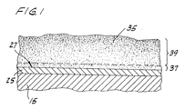
- Fig. 1 shows a cut-away cross-sectional view of a silicon body immersed in an etchant.
- Fig. 2 shows SiO 2 etch rate versus [NH 4 OH] in the absence of a megasonic field with the [NH 4 OH] ranging from about 500 ppm to about 5000 ppm and temperature ranging from about 30 °C to about 70°C.
- Fig. 3 shows SiO 2 etch rate versus [NH 4 OH] in the presence of a megasonic field with the [NH 4 OH] ranging from about 500 ppm to about 5000 ppm and temperature ranging from about 30°C to about 80°C.
- silicon is intended to include within its scope both single crystal silicon and polycrystalline silicon.
- etch rate refers to the change in the thickness of a silicon dioxide layer per unit of time, where the thickness is measured as the distance perpendicular to the surface of the silicon dioxide substrate.
- silicon body refers to any configuration or shape of silicon which comprises a silicon dioxide layer overlying a silicon substrate. Although silicon wafers are exemplary of and included within the scope of the term “silicon body,” the application of the invention is not limited to silicon wafers.
- silicon dioxide is etched from a silicon dioxide layer 25 overlying a silicon substrate 15 comprising silicon at a reaction surface 27.
- the reaction surface 27 is defined by the interface between the silicon dioxide layer 25 and an etchant solution 35.
- the concentration of etchant at the reaction surface 27 becomes depleted, and a concentration boundary layer 37 forms within the solution 35 between the reaction surface 27 and the bulk solution 39.
- the etchant must diffuse through the concentration boundary layer 37 in order to react with the silicon dioxide at the reaction surface 27.
- the etch rate of the silicon dioxide layer 25 may be limited by either the rate of the etching reaction or the rate of diffusion of reactants to the reaction surface 27.
- the etchant can diffuse through the concentration boundary layer 37 at a rate which is relatively faster than the rate at which the etchant is consumed in the etching reaction, there will be an excess of etchant at the reaction surface 27 and the etch rate will be limited by the rate of the etching reaction.
- the diffusion of etchant from the bulk solution 39 to the reaction surface 27 cannot keep pace with the consumption of etchant at the reaction surface, then the etch rate will be limited by the rate of diffusion.
- the rate of diffusion is directly proportional to the concentration of etchant in the bulk solution 39.
- a diffusion-rate-limiting threshold concentration of etchant in the bulk solution 39 is defined for a given temperature as that concentration above which the etch rate is limited by the rate of the etching reaction, and below which the etch rate is limited by diffusion of etchant to the reaction surface 27. If the etch rate is limited by the etching reaction rate, it is possible to control etch rate by the temperature of the solution 35 independent of the concentration of etchant. Conversely, if the etch rate is limited by diffusion, control of the etch rate is dependent upon temperature, upon the thickness of the concentration boundary layer 37 which defines the diffusion path length, and upon the concentration of etchant in the bulk solution 39.
- the silicon dioxide layer is chemically etched by an etchant in the presence of a megasonic field.
- Any chemical etchant may be used, including acidic and caustic etchants.
- Alkaline etchants comprising hydroxyl ions, such as ammonium hydroxide, tetramethyl ammonium hydroxide, potassium hydroxide or sodium hydroxide, are generally favored for many applications.
- An aqueous ammonium hydroxide solution is exemplary of the alkaline hydroxyl etchants, all of which substantially dissociate into hydroxyl ions under the conditions known and used in the art.
- the megasonic field may be generated by methods known in the art, including for example, using single-tank or double-tank megasonic cleaning apparatus.
- the frequency of the megasonic field preferably ranges from about 700 kHz to about 1200 kHz, and most preferably from about 840 kHz to about 875 kHz.
- the power of the megasonic field which is applied to the silicon bodies being etched is not narrowly critical, but can generally range from about 2 W per body to about 30 W per body, and preferably ranges from about 5 W per body to about 10 W per body.
- the total power being supplied to a bath of twenty-five silicon wafers being etched preferably ranges from about 100W to about 200W, and most preferably about 150W.
- the total power supplied to the megasonic transducer will generally need to be greater than the total power being applied to the bath in which the wafers are situated due to operational constraints, heat losses and other inefficiencies associated with the various megasonic cleaning apparatus.
- the power supplied to a single-tank megasonic cleaning apparatus rated at 300 W is typically limited to about 90% of its rated power --- about 270 W.
- the power supplied to the etchant bath would be about 216 W and the megasonic power applied to twenty-five wafers in the bath would be about 9 W per wafer.
- the silicon body is preferably orientated in the etching bath in a manner which allows for accoustic streaming of the etchant over the dioxide layer being etched when megasonics is applied.
- the wafers are preferably oriented in the etch-bath such that the surface of the wafer is in-line with (ie, parallel to) the direction in which the sound waves are transmitted through the etchant.
- Etching the silicon dioxide layer in the presence of a megasonic field substantially affects the manner and mechanism by which the etch-rate can be controlled.
- Figures 2 and 3 show SiO 2 etch rate versus concentration of NH 4 OH over similar temperature and concentration ranges with megasonics off and on, respectively. With megasonics off (Fig. 2), the etch rate is dependent upon the concentration of NH 4 OH and is under diffusion control. With megasonics on (Fig. 3), however, the etch rate is independent of the concentration of NH 4 OH and under reaction rate control. Without being bound by theory, the megasonic field appears to reduce the thickness of the concentration boundary layer 37 to create a shorter diffusion path length.
- the thickness of the concentration boundary layer 37 ranges from about 50 to about 100 ⁇ m in the absence of a megasonic field, whereas the boundary layer thickness is about 1 ⁇ m in the presence of a megasonic field.
- the diffusion-rate-limiting threshold concentration of etchant in the bulk solution 39 is reduced relative to its value in the absence of a megasonic field. That is, when a megasonic field is applied, the silicon dioxide etch rate becomes diffusion limited (ie, transitions from being reaction rate limited) at comparatively lower bulk concentrations of etchant.
- SiO 2 etch rates can be controlled independent of concentration using a dilute ammonium etchant at concentrations less than about 3000 ppm, but above the etchant's diffusion-rate-limiting threshold concentration for a particular temperature. Operating at such lower concentrations can be advantageous over prior art methods with respect to being less expensive and less corrosive.
- etch rates ranging from less than 5 x 10 -5 ⁇ m/min (0.5 ⁇ /min) to about 4 x 10 -4 ⁇ m/min (4 ⁇ /min) are achievable using an ammonium hydroxide etchant at concentrations less than about 5,000 ppm over a temperature range of 30°C to 80°C.
- these etch rates were realized in an SC1 system in which the ratio of NH 4 OH:H 2 O 2 :H 2 O ranges, respectively, from about 1:100:500 to about 1:10:50 by volume of commercially available reagent solutions, typically supplied as 28-30 wt% NH 4 OH in water and as 30-35 wt% H 2 O 2 in water.
- the ratios of ammonium hydroxide and hydrogen peroxide are expressed relative to water, but independent of each other. That is, in the SC1 solution described above, the ratio of NH 4 OH:H 2 O ranges from about 1:500 to about 1:50, the ratio of H 2 O 2 :H 2 O is about 1:5, and both of these ratios (NH 4 OH:H 2 O and H 2 O 2 :H 2 O) are independent of each other. Expressed in parts per million, the concentration of NH 4 OH in the SC1 solution described above ranges from about 550 ppm to about 5,500 ppm by weight relative to water.
- the etchant concentration while operating within the reaction-rate controlled regime using an aqueous alkaline etchant is preferably less than about 3000 ppm and more preferably less than about 1000 ppm by weight relative to water.
- Exemplary aqueous ammonium hydroxide etchant solutions would have ratios of NH 4 OH:H 2 O of 1:100 (for about 3000 ppm) and of 1:300 (for 1000 ppm) by volume of commercially available reagents.
- the silicon dioxide layer can also be etched at acceptable rates in the presence of a megasonic field while operating within the diffusion-controlled regime, where the etchant concentration is less than the diffusion-limiting threshold concentration for the temperature at which the silicon dioxide is being etched.
- the etchant concentration is preferably less than about 300 ppm by weight relative to water and more preferably less than about 100 ppm for temperatures ranging from about 30°C to about 80°C.
- the concentration of aqueous alkaline hydroxyl ion etchants preferably ranges from about 10 ppm to about 100 ppm and more preferably from about 30 ppm to about 100 ppm for temperatures ranging from about 30°C to about 80°C.
- the concentration of such etchants most preferably ranges from about 50 ppm to about 80 ppm at a temperature of about 70°C.
- silicon dioxide etch rates ranging from about 3 x 10 -5 ⁇ m/min (0.3 ⁇ /min) to about 4 x 10 -4 ⁇ m/min (4.0 ⁇ /min) are achievable.
- these etch rates are controllable to within about 2 x 10 -5 ⁇ m/min (0.2 ⁇ /min) of a desired or target etch rate, R etch .
- R etch a desired or target etch rate
- the use of such very dilute etchant solutions in conjunction with a megasonic system allows for relatively lower etch rates and a corresponding greater degree of control over the etching process.
- Using dilute etchants also results in less variation in concentration of etchant, and therefore, in more uniform etching.
- the uniform, controllable and low etch rates provide an opportunity to discontinue the etching reaction in a precise and controllable manner.
- dilute concentrations of etchant are substantially less expensive and less caustic.
- the present invention could be used in applications where the thickness of the silicon dioxide layer 25 is to be decreased more than 0.1 ⁇ m, the invention is preferable suited to applications requiring a decrease of less than 0.1 ⁇ m, and most preferably decreases in thickness ranging from about 5 x 10 -4 ⁇ m (5 ⁇ ) to about 5 x 10 -3 ⁇ m (50 ⁇ ).
- Controlling the etch rate to within about 2 x 10 -5 ⁇ m/min (0.2 ⁇ /min) of a desired etch rate further facilitates the controlled decrease in thickness of a silicon dioxide layer, as well as the controlled discontinuance of the etching before the silicon substrate is exposed to the etchant.
- the etch rate can be controllably discontinued when the thickness of the silicon dioxide layer is within about 5 x 10 -4 ⁇ m (5 ⁇ ) of a thickness, t, or equivalently, to within about one or two monolayers of silicon dioxide.
- alkaline etching and oxidizing of the silicon body occurs sequentially in separate baths. Specifically, the surface of a silicon body is cleaned by first chemically etching the silicon dioxide layer overlying the silicon substrate with an etchant in a first megasonic bath and in the absence of an oxidant.
- the surface of the silicon body is preferably hydrophilic before it is etched.
- the surface is hydrophobic, it is preferable to expose the surface to an oxidant, such as ozone, prior to etching to achieve a surface which is hydrophilic in nature.
- the etching is preferably diffusion-rate limited rather than reaction-rate limited.
- the etching is carried out in a megasonic bath with an etchant concentration less than the diffusion-limiting threshold concentration for the temperature at which the silicon dioxide is being etched.
- the silicon dioxide layer is preferably etched until the thickness of the silicon dioxide layer ranges from about 0.2 nm (2 ⁇ ) to about 1.0 nm (10 ⁇ ), but in any event, the etching is discontinued before the silicon substrate is exposed to the etchant. The etching results in an etched silicon body.
- the silicon substrate of the etched silicon body is oxidized with an oxidant in a second bath, preferably until the thickness of the silicon dioxide layer ranges from about 1.0 nm (10 ⁇ ) to about 1.5 nm (15 ⁇ ).
- the oxidant preferably comprises ozone at concentrations ranging from about 50 ppb to about 50 ppm.
- the etched silicon body is exposed to a ozone at a concentration of about 15 ppm for about 5 minutes at room temperature. The oxidizing results in an oxidized silicon body.
- the oxidized silicon body is then rinsed, and preferably, the etching and oxidizing steps detailed above are repeated several times to ensure rigorous cleaning of the surface of the silicon body.
- the etch-rinse-oxidize-rinse cycle can be repeated as many times as necessary to effect cleaning of the silicon body surface. For cleaning single-crystal silicon wafers as a part of wafer or device manufacturing processes, two to six etching-oxidizing cycles are generally sufficient.
- the oxidized silicon body is again rinsed, and then dried, preferably in an isopropyl alcohol vapor dryer.
- the thickness of the silicon dioxide layer may be measured by several direct or indirect methods known in the art. Exemplary direct methods include ellipsometry and photo-electron spectrometry. In one indirect method, the time required to etch the silicon dioxide layer at a known etch rate is measured, and the average thickness is calculated therefrom. In an alternative indirect method, the entire silicon dioxide layer is etched from the substrate, and the silica content of the etchant solution is determined. Vepa et al., A Method for Native Oxide Thickness Measurement, Electrochem. Soc. Proc., Vol. 95-20, pp. 358-365 (1995).
- a further embodiment of the present invention relates to an improvement in the SC1 cleaning step of the well known RCA method.
- the surface of a silicon body is cleaned by chemically etching the silicon dioxide layer overlying the silicon substrate with an etchant in a megasonic bath which comprises a dilute concentration of etchant and an oxidant.
- an etchant in a megasonic bath which comprises a dilute concentration of etchant and an oxidant.
- the oxidant in the bath simultaneously oxidizes the silicon substrate.
- etchant aqueous ammonium hydroxide and hydrogen peroxide are used as the etchant and oxidant, respectively.
- preferred concentrations of etchant ranging from about 10 ppm by weight relative to water to about 100 ppm are achieved using ratios of NH 4 OH:H 2 O 2 :H 2 O ranging from about 1:100:28,000 to about 1:100:3000, respectively, by volume of commercially available reagent solutions, typically supplied as 28-30 wt% NH 4 OH in water and as 30-35 wt% H 2 O 2 in water.
- these preferred concentrations are achieved using an SC1 solution in which the ratio of NH 4 OH:H 2 O ranges from about 1:28,000 to about 1:3000, the ratio of H 2 O 2 :H 2 O ranges from about 1:280 to about 1:30, and both of these ratios (NH 4 OH:H 2 O and H 2 O 2 :H 2 O) are independent of each other.
- Concentrations of etchant ranging from about 30 ppm by weight relative to water to about 100 ppm are achieved using ratios of NH 4 OH:H 2 O2:H 2 O ranging from about 1:100:9,000 to about 1:100:3000, respectively, by volume of commercially available reagent solutions, typically supplied as 28-30 wt% NH 4 OH in water and as 30-35 wt% H 2 O 2 in water.
- the silicon body may be subsequently exposed to the SC2 solution in accordance with the known RCA method.
- Gate oxides are known in the art and are used in devices such as NMOS and PMOS field effect transistors (FET's). Gate oxides comprise a thin silicon dioxide layer overlying a silicon substrate. Typically, the thickness of the silicon dioxide layer on such thin gate oxides ranges from about 8 x 10 -3 ⁇ m (80 ⁇ ) to about 1 x 10 2 ⁇ m (100 ⁇ ). Recent advances in gate oxide technologies require silicon dioxide layers ranging from about 4 x10 -3 ⁇ m (40 ⁇ ) to about 5 x 10 -3 ⁇ m (50 ⁇ ). Further advances in technology for may ultimately require ultra thin silicon dioxide layers as thin as about 5 x 10 -4 (5 ⁇ ). Such ultra thin oxides may be achieved by the methods of this invention.
- inventions described herein may be used in both multiple bath systems which employ a single process step in each bath, or in single bath systems which employ multiple process steps in that single bath. Further, the embodiments of the present invention could be employed as continuous processes or as batch processes acting on either multiple or individual silicon bodies.
Landscapes
- Weting (AREA)
- Cleaning Or Drying Semiconductors (AREA)
- ing And Chemical Polishing (AREA)
Applications Claiming Priority (2)
| Application Number | Priority Date | Filing Date | Title |
|---|---|---|---|
| US08/749,906 US5919311A (en) | 1996-11-15 | 1996-11-15 | Control of SiO2 etch rate using dilute chemical etchants in the presence of a megasonic field |
| US749906 | 1996-11-15 |
Publications (2)
| Publication Number | Publication Date |
|---|---|
| EP0844650A2 true EP0844650A2 (de) | 1998-05-27 |
| EP0844650A3 EP0844650A3 (de) | 1999-05-26 |
Family
ID=25015712
Family Applications (1)
| Application Number | Title | Priority Date | Filing Date |
|---|---|---|---|
| EP97307698A Withdrawn EP0844650A3 (de) | 1996-11-15 | 1997-09-30 | Verfahren zum Aetzen von Sio2 und Verfahren zur Reinigung von Siliziumscheiben unter Verwendung von verdünnten Aetzmitteln und Megaschall |
Country Status (7)
| Country | Link |
|---|---|
| US (1) | US5919311A (de) |
| EP (1) | EP0844650A3 (de) |
| JP (1) | JPH10154690A (de) |
| KR (1) | KR19980042006A (de) |
| MY (1) | MY141358A (de) |
| SG (1) | SG55386A1 (de) |
| TW (1) | TW399255B (de) |
Cited By (9)
| Publication number | Priority date | Publication date | Assignee | Title |
|---|---|---|---|---|
| EP1005072A1 (de) * | 1998-11-19 | 2000-05-31 | Wacker Siltronic Gesellschaft für Halbleitermaterialien Aktiengesellschaft | Verfahren zur nasschemischen Behandlung von Halbleiterscheiben |
| EP0994505A3 (de) * | 1998-10-13 | 2000-07-19 | Kurita Water Industries Ltd. | Verfahren zur Reinigung von Substraten |
| WO2001013418A1 (en) * | 1999-08-16 | 2001-02-22 | Memc Electronic Materials, Inc. | A single-operation method of cleaning semiconductors after final polishing |
| WO2001026144A1 (en) * | 1999-10-01 | 2001-04-12 | Fsi International, Inc. | Methods for cleaning microelectronic substrates using ultradilute cleaning liquids |
| US6681781B2 (en) | 1999-05-13 | 2004-01-27 | Fsi International, Inc. | Methods for cleaning microelectronic substrates using ultradilute cleaning liquids |
| FR2923947A1 (fr) * | 2007-11-20 | 2009-05-22 | Inst Polytechnique Grenoble | Procede et dispositif de gravure selective. |
| WO2010133786A1 (fr) * | 2009-05-18 | 2010-11-25 | Institut Polytechnique De Grenoble | Procede de gravure d'un materiau en presence d'un gaz |
| EP3067949A1 (de) | 2015-03-09 | 2016-09-14 | Heraeus Deutschland GmbH & Co. KG | Leitfähige Polymer/Si-Schnittstellen auf der Rückseite von Solarzellen |
| EP3276693A1 (de) | 2016-07-28 | 2018-01-31 | Heraeus Deutschland GmbH & Co. KG | Solarzellen mit leitfähigen polymerpassivierungsschichten auf der rückseite |
Families Citing this family (19)
| Publication number | Priority date | Publication date | Assignee | Title |
|---|---|---|---|---|
| US6074960A (en) | 1997-08-20 | 2000-06-13 | Micron Technology, Inc. | Method and composition for selectively etching against cobalt silicide |
| KR100290703B1 (ko) * | 1997-08-26 | 2001-06-01 | 윤종용 | 정량공급조건을갖는반도체웨이퍼세정방법 |
| US6632321B2 (en) | 1998-01-06 | 2003-10-14 | Applied Materials, Inc | Method and apparatus for monitoring and controlling wafer fabrication process |
| US6429144B1 (en) * | 1999-12-28 | 2002-08-06 | Koninklijke Philips Electronics N.V. | Integrated circuit manufacture method with aqueous hydrogen fluoride and nitric acid oxide etch |
| US6403267B1 (en) * | 2000-01-21 | 2002-06-11 | Taiwan Semiconductor Manufacturing Company | Method for high transmittance attenuated phase-shifting mask fabrication |
| US7156927B2 (en) * | 2002-04-03 | 2007-01-02 | Fsi International, Inc. | Transition flow treatment process and apparatus |
| US20030232507A1 (en) * | 2002-06-12 | 2003-12-18 | Macronix International Co., Ltd. | Method for fabricating a semiconductor device having an ONO film |
| WO2005117138A1 (ja) * | 2004-05-28 | 2005-12-08 | Sharp Kabushiki Kaisha | 太陽電池用半導体基板とその製造方法および太陽電池 |
| US7655094B2 (en) * | 2004-07-07 | 2010-02-02 | Nano Om, Llc | Systems and methods for charging a cleaning solution used for cleaning integrated circuit substrates |
| US7731800B2 (en) * | 2004-07-07 | 2010-06-08 | Nano Om, Llc | Systems and methods for single integrated substrate cleaning and rinsing |
| KR100580117B1 (ko) * | 2004-09-03 | 2006-05-12 | 에스티마이크로일렉트로닉스 엔.브이. | 반도체 메모리 소자의 소자 분리막 형성방법 |
| US20060078850A1 (en) * | 2004-10-13 | 2006-04-13 | Suraj Puri | Systems, methods and compositions for promoting oral hygiene |
| US20060142689A1 (en) * | 2004-10-13 | 2006-06-29 | Suraj Puri | Systems, methods and compositions for cleaning wounds |
| FR2884647B1 (fr) * | 2005-04-15 | 2008-02-22 | Soitec Silicon On Insulator | Traitement de plaques de semi-conducteurs |
| US8741066B2 (en) * | 2007-02-16 | 2014-06-03 | Akrion Systems, Llc | Method for cleaning substrates utilizing surface passivation and/or oxide layer growth to protect from pitting |
| US7776713B2 (en) * | 2007-05-30 | 2010-08-17 | Macronix International Co., Ltd. | Etching solution, method of surface modification of semiconductor substrate and method of forming shallow trench isolation |
| US20090142247A1 (en) * | 2007-12-03 | 2009-06-04 | Applied Materials, Inc. | Chemical treatment to reduce machining-induced sub-surface damage in semiconductor processing components comprising silicon carbide |
| JP2010226089A (ja) * | 2009-01-14 | 2010-10-07 | Rohm & Haas Electronic Materials Llc | 半導体ウェハをクリーニングする方法 |
| US10553720B2 (en) * | 2016-11-29 | 2020-02-04 | Taiwan Semiconductor Manufacturing Company, Ltd. | Method of removing an etch mask |
Family Cites Families (12)
| Publication number | Priority date | Publication date | Assignee | Title |
|---|---|---|---|---|
| US3893869A (en) * | 1974-05-31 | 1975-07-08 | Rca Corp | Megasonic cleaning system |
| US4339340A (en) * | 1975-11-26 | 1982-07-13 | Tokyo Shibaura Electric Co., Ltd. | Surface-treating agent adapted for intermediate products of a semiconductor device |
| US4264374A (en) * | 1978-09-25 | 1981-04-28 | International Business Machines Corporation | Cleaning process for p-type silicon surface |
| US5037481B1 (en) * | 1987-04-29 | 1993-05-11 | Verteq, Inc. | Megasonic cleaning method |
| US4804007A (en) * | 1987-04-29 | 1989-02-14 | Verteq, Inc. | Cleaning apparatus |
| US5090432A (en) * | 1990-10-16 | 1992-02-25 | Verteq, Inc. | Single wafer megasonic semiconductor wafer processing system |
| US5279316A (en) * | 1992-08-18 | 1994-01-18 | P.C.T. Systems, Inc. | Multiprocessing sonic bath system for semiconductor wafers |
| US5439569A (en) * | 1993-02-12 | 1995-08-08 | Sematech, Inc. | Concentration measurement and control of hydrogen peroxide and acid/base component in a semiconductor bath |
| US5464480A (en) * | 1993-07-16 | 1995-11-07 | Legacy Systems, Inc. | Process and apparatus for the treatment of semiconductor wafers in a fluid |
| JP2586304B2 (ja) * | 1993-09-21 | 1997-02-26 | 日本電気株式会社 | 半導体基板の洗浄液および洗浄方法 |
| US5656097A (en) * | 1993-10-20 | 1997-08-12 | Verteq, Inc. | Semiconductor wafer cleaning system |
| US5516730A (en) * | 1994-08-26 | 1996-05-14 | Memc Electronic Materials, Inc. | Pre-thermal treatment cleaning process of wafers |
-
1996
- 1996-11-15 US US08/749,906 patent/US5919311A/en not_active Expired - Fee Related
-
1997
- 1997-09-29 SG SG1997003613A patent/SG55386A1/en unknown
- 1997-09-30 EP EP97307698A patent/EP0844650A3/de not_active Withdrawn
- 1997-10-06 TW TW086114587A patent/TW399255B/zh active
- 1997-10-10 MY MYPI97004757A patent/MY141358A/en unknown
- 1997-10-31 KR KR1019970057312A patent/KR19980042006A/ko not_active Withdrawn
- 1997-11-14 JP JP9313233A patent/JPH10154690A/ja not_active Withdrawn
Cited By (18)
| Publication number | Priority date | Publication date | Assignee | Title |
|---|---|---|---|---|
| EP0994505A3 (de) * | 1998-10-13 | 2000-07-19 | Kurita Water Industries Ltd. | Verfahren zur Reinigung von Substraten |
| US7172975B2 (en) | 1998-11-19 | 2007-02-06 | Siltronic Ag | Process for the wet chemical treatment of semiconductor wafers |
| EP1005072A1 (de) * | 1998-11-19 | 2000-05-31 | Wacker Siltronic Gesellschaft für Halbleitermaterialien Aktiengesellschaft | Verfahren zur nasschemischen Behandlung von Halbleiterscheiben |
| SG83159A1 (en) * | 1998-11-19 | 2001-09-18 | Wacker Siltronic Halbleitermat | Process for the wet chemical treatment of semiconductor wafers |
| US6681781B2 (en) | 1999-05-13 | 2004-01-27 | Fsi International, Inc. | Methods for cleaning microelectronic substrates using ultradilute cleaning liquids |
| US6799583B2 (en) | 1999-05-13 | 2004-10-05 | Suraj Puri | Methods for cleaning microelectronic substrates using ultradilute cleaning liquids |
| US6230720B1 (en) | 1999-08-16 | 2001-05-15 | Memc Electronic Materials, Inc. | Single-operation method of cleaning semiconductors after final polishing |
| WO2001013418A1 (en) * | 1999-08-16 | 2001-02-22 | Memc Electronic Materials, Inc. | A single-operation method of cleaning semiconductors after final polishing |
| WO2001026144A1 (en) * | 1999-10-01 | 2001-04-12 | Fsi International, Inc. | Methods for cleaning microelectronic substrates using ultradilute cleaning liquids |
| FR2923947A1 (fr) * | 2007-11-20 | 2009-05-22 | Inst Polytechnique Grenoble | Procede et dispositif de gravure selective. |
| WO2009071788A3 (fr) * | 2007-11-20 | 2009-07-23 | Inst Polytechnique Grenoble | Procede et dispositif de gravure selective |
| US8440092B2 (en) | 2007-11-20 | 2013-05-14 | Institut Polytechnique De Grenoble | Method for selective etching |
| WO2010133786A1 (fr) * | 2009-05-18 | 2010-11-25 | Institut Polytechnique De Grenoble | Procede de gravure d'un materiau en presence d'un gaz |
| US8828255B2 (en) | 2009-05-18 | 2014-09-09 | Institut Polytechnique De Grenoble | Method for etching a material in the presence of a gas |
| EP3067949A1 (de) | 2015-03-09 | 2016-09-14 | Heraeus Deutschland GmbH & Co. KG | Leitfähige Polymer/Si-Schnittstellen auf der Rückseite von Solarzellen |
| WO2016142434A1 (en) | 2015-03-09 | 2016-09-15 | Heraeus Deutschland GmbH & Co. KG | Conductive polymer/si interfaces at the back side of solar cells |
| EP3276693A1 (de) | 2016-07-28 | 2018-01-31 | Heraeus Deutschland GmbH & Co. KG | Solarzellen mit leitfähigen polymerpassivierungsschichten auf der rückseite |
| WO2018019949A1 (en) | 2016-07-28 | 2018-02-01 | Heraeus Deutschland Gmbh & Co Kg | Solar cells with conductive polymer passivation layers on the back side |
Also Published As
| Publication number | Publication date |
|---|---|
| US5919311A (en) | 1999-07-06 |
| JPH10154690A (ja) | 1998-06-09 |
| MY141358A (en) | 2010-04-16 |
| EP0844650A3 (de) | 1999-05-26 |
| TW399255B (en) | 2000-07-21 |
| SG55386A1 (en) | 1998-12-21 |
| KR19980042006A (ko) | 1998-08-17 |
Similar Documents
| Publication | Publication Date | Title |
|---|---|---|
| US5919311A (en) | Control of SiO2 etch rate using dilute chemical etchants in the presence of a megasonic field | |
| US4808259A (en) | Plasma etching process for MOS circuit pregate etching utiliizing a multi-step power reduction recipe | |
| US4885056A (en) | Method of reducing defects on semiconductor wafers | |
| US5567244A (en) | Process for cleaning semiconductor devices | |
| EP1737026B1 (de) | Verfahren zur Oberflächenbehandlung von III-V-Halbleitersubstraten und Verfahren zur Herstellung von III-V-Verbindungshalbleitern | |
| US5601656A (en) | Methods for cleaning silicon wafers with an aqueous solution of hydrofluoric acid and hydriodic acid | |
| JPH1092777A (ja) | 半導体ウェハの製造方法 | |
| US5964953A (en) | Post-etching alkaline treatment process | |
| US6663674B2 (en) | Method of handling a silicon wafer | |
| EP0926714A1 (de) | Wasser zum Lagern von Silicium-Wafern und Verfahren zum Lagern von Silicium-Wafern | |
| US7153782B2 (en) | Effective solution and process to wet-etch metal-alloy films in semiconductor processing | |
| WO1994027314A1 (en) | Method for semiconductor processing using mixtures of hf and carboxylic acid | |
| TWI501302B (zh) | 阻擋層的去除方法和裝置 | |
| US20040266191A1 (en) | Process for the wet-chemical surface treatment of a semiconductor wafer | |
| CN103985670B (zh) | 阻挡层的去除方法和装置 | |
| US6541391B2 (en) | Methods of cleaning surfaces of copper-containing materials, and methods of forming openings to copper-containing substrates | |
| EP1132951A1 (de) | Verfahren zur Reinigung von Silizium vor der Gate Oxidierung | |
| JP4857738B2 (ja) | 半導体ウエーハの洗浄方法および製造方法 | |
| JPH0786220A (ja) | 半導体ウエハの洗浄方法 | |
| JP3257518B2 (ja) | シリコンウエーハを液中で保管する方法 | |
| US6063205A (en) | Use of H2 O2 solution as a method of post lap cleaning | |
| JP2715086B2 (ja) | 半導体ウェーハに対する熱酸化膜の形成方法 | |
| JP3535539B2 (ja) | 半導体装置の製造方法 | |
| JPH0621034A (ja) | 半導体基板の洗浄液 | |
| JP2639008B2 (ja) | 半導体基板の洗浄方法 |
Legal Events
| Date | Code | Title | Description |
|---|---|---|---|
| PUAI | Public reference made under article 153(3) epc to a published international application that has entered the european phase |
Free format text: ORIGINAL CODE: 0009012 |
|
| AK | Designated contracting states |
Kind code of ref document: A2 Designated state(s): DE FR GB IT |
|
| AX | Request for extension of the european patent |
Free format text: AL;LT;LV;RO;SI |
|
| PUAL | Search report despatched |
Free format text: ORIGINAL CODE: 0009013 |
|
| AK | Designated contracting states |
Kind code of ref document: A3 Designated state(s): AT BE CH DE DK ES FI FR GB GR IE IT LI LU MC NL PT SE |
|
| AX | Request for extension of the european patent |
Free format text: AL;LT;LV;RO;SI |
|
| 17P | Request for examination filed |
Effective date: 19990911 |
|
| AKX | Designation fees paid |
Free format text: DE FR GB IT |
|
| 17Q | First examination report despatched |
Effective date: 20020114 |
|
| STAA | Information on the status of an ep patent application or granted ep patent |
Free format text: STATUS: THE APPLICATION IS DEEMED TO BE WITHDRAWN |
|
| 18D | Application deemed to be withdrawn |
Effective date: 20020525 |