EP0844652A1 - Integrierbarer Kondensator Verfahren zu seiner Herstellung sowie Speicherfeld unter Verwendung des Kondensators - Google Patents
Integrierbarer Kondensator Verfahren zu seiner Herstellung sowie Speicherfeld unter Verwendung des Kondensators Download PDFInfo
- Publication number
- EP0844652A1 EP0844652A1 EP97118283A EP97118283A EP0844652A1 EP 0844652 A1 EP0844652 A1 EP 0844652A1 EP 97118283 A EP97118283 A EP 97118283A EP 97118283 A EP97118283 A EP 97118283A EP 0844652 A1 EP0844652 A1 EP 0844652A1
- Authority
- EP
- European Patent Office
- Prior art keywords
- electrode
- etching
- layer
- metal
- dielectric layer
- Prior art date
- Legal status (The legal status is an assumption and is not a legal conclusion. Google has not performed a legal analysis and makes no representation as to the accuracy of the status listed.)
- Withdrawn
Links
- 239000003990 capacitor Substances 0.000 title claims abstract description 52
- 238000004519 manufacturing process Methods 0.000 title claims abstract description 15
- 238000000034 method Methods 0.000 title claims description 32
- 230000015654 memory Effects 0.000 title claims description 16
- 229910052751 metal Inorganic materials 0.000 claims abstract description 54
- 239000002184 metal Substances 0.000 claims abstract description 54
- 238000005530 etching Methods 0.000 claims abstract description 50
- 238000001312 dry etching Methods 0.000 claims abstract description 5
- 239000000126 substance Substances 0.000 claims abstract description 5
- 150000001875 compounds Chemical class 0.000 claims description 7
- 239000007789 gas Substances 0.000 claims description 6
- 150000008282 halocarbons Chemical class 0.000 claims description 6
- -1 hydrogen halides Chemical class 0.000 claims description 6
- 229910021332 silicide Inorganic materials 0.000 claims description 5
- FVBUAEGBCNSCDD-UHFFFAOYSA-N silicide(4-) Chemical compound [Si-4] FVBUAEGBCNSCDD-UHFFFAOYSA-N 0.000 claims description 5
- 238000000227 grinding Methods 0.000 claims description 4
- 239000000203 mixture Substances 0.000 claims description 4
- 238000001020 plasma etching Methods 0.000 claims description 3
- WFKWXMTUELFFGS-UHFFFAOYSA-N tungsten Chemical compound [W] WFKWXMTUELFFGS-UHFFFAOYSA-N 0.000 claims description 3
- 229910052721 tungsten Inorganic materials 0.000 claims description 3
- 239000010937 tungsten Substances 0.000 claims description 3
- RYGMFSIKBFXOCR-UHFFFAOYSA-N Copper Chemical compound [Cu] RYGMFSIKBFXOCR-UHFFFAOYSA-N 0.000 claims description 2
- XUIMIQQOPSSXEZ-UHFFFAOYSA-N Silicon Chemical compound [Si] XUIMIQQOPSSXEZ-UHFFFAOYSA-N 0.000 claims description 2
- 229910052787 antimony Inorganic materials 0.000 claims description 2
- WATWJIUSRGPENY-UHFFFAOYSA-N antimony atom Chemical compound [Sb] WATWJIUSRGPENY-UHFFFAOYSA-N 0.000 claims description 2
- 229910052796 boron Inorganic materials 0.000 claims description 2
- 229910052802 copper Inorganic materials 0.000 claims description 2
- 239000010949 copper Substances 0.000 claims description 2
- 229910052736 halogen Inorganic materials 0.000 claims description 2
- 150000002367 halogens Chemical class 0.000 claims description 2
- 229910052739 hydrogen Inorganic materials 0.000 claims description 2
- 239000001257 hydrogen Substances 0.000 claims description 2
- 229910052710 silicon Inorganic materials 0.000 claims description 2
- 239000010703 silicon Substances 0.000 claims description 2
- ZOXJGFHDIHLPTG-UHFFFAOYSA-N Boron Chemical compound [B] ZOXJGFHDIHLPTG-UHFFFAOYSA-N 0.000 claims 1
- AZDRQVAHHNSJOQ-UHFFFAOYSA-N alumane Chemical class [AlH3] AZDRQVAHHNSJOQ-UHFFFAOYSA-N 0.000 claims 1
- 229910001507 metal halide Inorganic materials 0.000 claims 1
- 150000005309 metal halides Chemical class 0.000 claims 1
- 229910044991 metal oxide Inorganic materials 0.000 claims 1
- 150000004706 metal oxides Chemical class 0.000 claims 1
- 238000001465 metallisation Methods 0.000 claims 1
- 229920000642 polymer Polymers 0.000 abstract description 2
- 239000004020 conductor Substances 0.000 description 7
- 229910052782 aluminium Inorganic materials 0.000 description 3
- XAGFODPZIPBFFR-UHFFFAOYSA-N aluminium Chemical compound [Al] XAGFODPZIPBFFR-UHFFFAOYSA-N 0.000 description 3
- 239000003795 chemical substances by application Substances 0.000 description 3
- 239000003973 paint Substances 0.000 description 3
- OKTJSMMVPCPJKN-UHFFFAOYSA-N Carbon Chemical compound [C] OKTJSMMVPCPJKN-UHFFFAOYSA-N 0.000 description 2
- VYPSYNLAJGMNEJ-UHFFFAOYSA-N Silicium dioxide Chemical compound O=[Si]=O VYPSYNLAJGMNEJ-UHFFFAOYSA-N 0.000 description 2
- 230000004888 barrier function Effects 0.000 description 2
- 238000005516 engineering process Methods 0.000 description 2
- 230000006870 function Effects 0.000 description 2
- YCKRFDGAMUMZLT-UHFFFAOYSA-N Fluorine atom Chemical compound [F] YCKRFDGAMUMZLT-UHFFFAOYSA-N 0.000 description 1
- 229910016006 MoSi Inorganic materials 0.000 description 1
- 229910052581 Si3N4 Inorganic materials 0.000 description 1
- 229910004298 SiO 2 Inorganic materials 0.000 description 1
- 229910008484 TiSi Inorganic materials 0.000 description 1
- 239000000654 additive Substances 0.000 description 1
- 230000009286 beneficial effect Effects 0.000 description 1
- 229910052799 carbon Inorganic materials 0.000 description 1
- 238000011161 development Methods 0.000 description 1
- 230000018109 developmental process Effects 0.000 description 1
- 239000007772 electrode material Substances 0.000 description 1
- 230000002349 favourable effect Effects 0.000 description 1
- 229910052731 fluorine Inorganic materials 0.000 description 1
- 239000011737 fluorine Substances 0.000 description 1
- 150000004820 halides Chemical class 0.000 description 1
- 238000009413 insulation Methods 0.000 description 1
- 239000004922 lacquer Substances 0.000 description 1
- 238000004377 microelectronic Methods 0.000 description 1
- 229920002120 photoresistant polymer Polymers 0.000 description 1
- 238000002360 preparation method Methods 0.000 description 1
- 239000004065 semiconductor Substances 0.000 description 1
- 235000012239 silicon dioxide Nutrition 0.000 description 1
- 239000000377 silicon dioxide Substances 0.000 description 1
- HQVNEWCFYHHQES-UHFFFAOYSA-N silicon nitride Chemical compound N12[Si]34N5[Si]62N3[Si]51N64 HQVNEWCFYHHQES-UHFFFAOYSA-N 0.000 description 1
- 238000003860 storage Methods 0.000 description 1
Images
Classifications
-
- H—ELECTRICITY
- H10—SEMICONDUCTOR DEVICES; ELECTRIC SOLID-STATE DEVICES NOT OTHERWISE PROVIDED FOR
- H10B—ELECTRONIC MEMORY DEVICES
- H10B12/00—Dynamic random access memory [DRAM] devices
- H10B12/01—Manufacture or treatment
- H10B12/02—Manufacture or treatment for one transistor one-capacitor [1T-1C] memory cells
- H10B12/03—Making the capacitor or connections thereto
-
- H—ELECTRICITY
- H10—SEMICONDUCTOR DEVICES; ELECTRIC SOLID-STATE DEVICES NOT OTHERWISE PROVIDED FOR
- H10D—INORGANIC ELECTRIC SEMICONDUCTOR DEVICES
- H10D1/00—Resistors, capacitors or inductors
- H10D1/60—Capacitors
- H10D1/68—Capacitors having no potential barriers
Definitions
- the invention relates to an integrable capacitor a dielectric layer and two electrodes, as it is in particular for integrated circuits with microstructures is used, as well as a process for its preparation and a memory field in which capacitors according to the invention are used will.
- Capacitors are commonly used in integrated circuits executed in a planar, trench or stacked arrangement. Such capacitors are used in connection with a transistor to form memory cells in Semiconductor memories. Here, a large number of memory cells arranged in a storage field.
- the dielectric layer which is located between the electrically conductive electrode materials of such capacitors, for example from SiO 2 or Si 3 N 4 .
- Such a dielectric layer does indeed have favorable electrical properties, such as a high degree of insulation and high dielectric, on the other hand, the production is quite complex and always requires at least one additional production step, since the dielectric layer is applied to the surface of the electrode after the production .
- the invention has for its object to provide a capacitor with a dielectric layer and two electrodes - in particular for use in integrated circuits with a microstructure - which has a dielectric layer which is particularly easy to produce and has good electrical properties. Another object is to specify a manufacturing method for such a capacitor and a memory array using the capacitor.
- the object is achieved by the capacitor according to claim 1.
- the task is solved the method of claim 13.
- Etching processes are usually used to produce structured surfaces in integrated circuits.
- An overview of suitable etching processes can be found, for example, in D. Widmann, H. Mader and H. Friedrich, Technology of Highly Integrated Circuits, 2nd Edition, Springer-Verlag Berlin, 1996, and K. Schade, Microelectronics Technology, 1st Edition, Verlagtechnik, Berlin, 1991.
- a mask made of photoresist for example, is applied to the metal layer and covers the areas that are not to be etched - that is, the later electrodes.
- the etching process itself is preferably carried out using a dry etching process in order to achieve an anisotropic etching process.
- the surfaces of the electrodes exposed by the etching are rarely purely metallic surfaces. Rather, they have deposits of etched products that were previously completely removed before the electrodes were further processed in order to obtain metallic surfaces. A dielectric layer made of silicon dioxide, silicon nitride or the like was then applied to these metallic surfaces in order to produce capacitors.
- etching process is carried out so that when Etching out an electrode from a metal layer on the surfaces of the electrode accessible to the etchant a continuous dielectric layer is formed which serve directly as a dielectric in a capacitor can.
- This dielectric layer consists of etched products of the metal and / or polymeric structures that develop during of the etching process and deposit on the electrode surface.
- etching process Dry etching methods used, such as basically in the literature references mentioned above are described.
- the etching is particularly preferred by plasma etching.
- the etchant which is preferably an etching gas, is selected as a function of the structure to be etched and in particular as a function of the metal layer to be etched. Suitable etchants are generally known to the person skilled in the art and are also listed, for example, in the literature references mentioned.
- the metal layers to be etched can consist essentially of aluminum or tungsten, for example. In the case of aluminum, fluorine-containing etchants are unfavorable, since low-volatility etch products are formed.
- suitable etching agents are halogens such as F 2 , Cl 2 , Br 2 , I 2 , hydrogen halides such as HF, HCl, HBr, HI, boron halogen compounds, silicon or antimony or halogenated hydrocarbons.
- halogens such as F 2 , Cl 2 , Br 2 , I 2
- hydrogen halides such as HF, HCl, HBr, HI
- boron halogen compounds silicon or antimony or halogenated hydrocarbons.
- a single compound or several compounds of each of the groups mentioned can be used, or mixtures of several compounds of the different groups.
- the etching agents can contain additives of other commonly used compounds such as non-halogenated hydrocarbons.
- halogenated Hydrocarbons are carbon-containing compounds and especially halogenated Hydrocarbons, optionally in combination with other compounds commonly used in etching, used as etching gas, arise during the etching process polymeric structures on the surface of the etched metal layer.
- halogenated hydrocarbons for example from halogenated carbon chains.
- Other etching products formed in the course of the etching process e.g. Halides or oxides of the etched Be metal.
- the etching process is carried out in such a way that a continuous dielectric layer, which consists of a polymeric structure and / or etching products of the metal, is deliberately produced on the etched surfaces of the first electrode, which is etched from a metal layer.
- the composition of the layer and thus its physicochemical properties as well as its layer thickness are determined by a suitable choice of the etchant and the process parameters during the etching. In this way, a very simple and targeted production of the dielectric layer between a first and a second electrode in a capacitor is possible.
- the first is Electrode cylindrical and the dielectric layer formed in the shape of a hollow cylinder on the cylinder jacket.
- the cylindrical electrode is expedient in an anisotropic Etching process produced in the approximately vertical Flank areas of the structured surfaces are generated, the cylinder axis being perpendicular to the surface of the Basic structure runs on which the metal layer to be etched was ordered.
- the dielectric is Layer easy to make and it will be beneficial Arrangement of the capacitor achieved, which is characterized by good Characterized contactability and low space consumption.
- Around the second electrode is formed around the dielectric layer.
- the second electrode can be designed as a metal layer which serves several or all of the first electrodes as a common counterelectrode.
- the contact points are advantageously arranged at the ends of the electrodes in the direction of the cylinder axes. This arrangement results in advantageous supply lines to the capacitor.
- the The height of the second electrode is preferably less than the height the first electrode. This can be achieved, for example be that the second electrode is removed so far is that their top is lower than the top of the first electrode.
- the second electrode is expediently passed through Grinding or etching removed.
- a conductive layer can advantageously be arranged on the upper side of the second electrode.
- the conductive layer consists of a metal silicide, such as MoSi 2 , WSi 2 , TaSi 2 or TiSi 2 .
- This electrically conductive layer particularly advantageously has a lower resistance than the second electrode.
- a further conductive layer can be arranged on the conductive layer. This is low-resistance and consists, for example, of a metal such as aluminum or copper.
- the lower electrically conductive layer serves as a barrier layer for the upper conductive layer.
- the layer structure with different resistors corresponds to an arrangement with resistors connected in parallel. It is again advantageous if the height of the second electrode plus the conductive layer and possibly another conductive layer is less than the height of the first electrode.
- the capacitors according to the invention can advantageously after the method according to claim 13 are produced.
- a metal layer is first applied to a basic structure.
- the basic structure can be, for example, a conductor track system be.
- This metal layer is etched so that a first electrode arises and on its more accessible to etching Surface a polymer structure and / or etching products of the Metal are formed as a dielectric layer.
- a second electrode is attached so that the first and second electrodes through the dielectric layer from each other are separated.
- a metal layer is etched and capacitors a dielectric layer on the etched surfaces formed, to which a second electrode is arranged adjacent becomes.
- the capacitor is thus in just two Steps. This is a significant time and Cost savings connected.
- the metal layer is advantageously anisotropically etched, the dielectric layer being formed on the vertical flanks of the first electrode.
- the process steps mentioned above can be useful an anisotropic etching back or grinding back of the second Connect the electrode, the metal layer of the second Electrode is etched deeper than that of the first to be reliable to avoid a short circuit to the first electrode.
- at least one can be electrically on the second electrode conductive layer can be applied.
- the method according to the invention is not only suitable for production individual capacitors, but especially for simultaneous production of several capacitors according to the invention, for example in a memory field that consists of several side by side capacitors and usual other components exist, are attached.
- Such memory fields are also the subject of the invention.
- a plurality of first electrodes serving as a counter electrode Metal layer is in an advantageous embodiment a connection area formed in that the distance between adjacent first electrodes is enlarged to sufficient space for the base point of a bond wire create.
- the embodiment shown represents an integrated one Circuit in the form of an arrangement of several capacitors that form a memory array. Below the capacitors transistors are arranged, but not in the figures are shown.
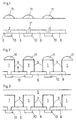
- the conductor tracks 10 form the basic structure an integrated circuit. Are among them other components (not shown) such as transistors and further conductor tracks. There are three conductor tracks 10 evenly spaced from each other. About that is the next structure in the areas between the traces 10 each have a dielectric layer 6 arranged, hereinafter referred to as the basic structure dielectric becomes. A metal layer 1 'is arranged above this. Since that Basic structure dielectric 6 only in the spaces between the conductor tracks 10 is arranged, the metal layer is sufficient 1 'between them up to the conductor tracks 10. In these Areas 2 are electrically contacted. The Metal layer is made relatively high and on its surface just. Exactly over the contact areas 2 between the Metal layer 1 'and the conductor tracks 10 aligned the paint 11 of a paint mask.
- FIG. 2 shows the next intermediate stage of the manufacturing process.
- the surface of the metal layer 1 'became anisotropic etched, the areas provided with the lacquer 11 Surface are excluded from the etching process.
- the metal layer 1 ' is in the stage shown in Fig. 2 up to etched down the basic structure dielectric 6. To this Individual first electrodes are made of the metal layer 1 ' 1 emerged. On their flanks has been etched through a dielectric layer 3 is formed, which by appropriate Selection of the etching gas and the process parameters during of the etching in its composition and layer thickness was generated.
- the paint 11 is removed and a further metal layer 5 on the integrated circuit structure upset.
- this is metal layer 5 so high that they electrodes 1 towered over in height. It has a flat surface.
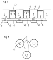
- Fig. 4 illustrates the further course of the process in which the metal layer 5 has been etched back so far that its surface 7 below the surfaces 8 of the first electrodes 1 lies. An upper end 9 of the dielectric layer 3 is thereby exposed.
- the described Metal layer 5 e.g. tungsten
- a second electrode 4 get that as a common counter electrode for several first Electrodes 1 is used.
- a thin silicide layer as an electrically conductive layer 12 applied.
- a second, low-resistance, electrically conductive layer 13 which is similar to the metal layer 5 in an anisotropic Etching process from the surfaces 8 of the first electrode 1 was removed and only over the silicide Regions 12 of the second electrode 4 extends.
- the barrier layer 12 and the layer 13 have one essential lower resistance than the metal layer of the second electrode 4. These two layers can be connected in parallel resistances.
- Electrodes 1 and 4 are the from Electrodes 1 and 4 and the dielectric layer 3 are formed Capacitors arranged regularly.
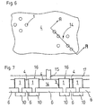
- FIG. 6 shows the top view of an arrangement of several Capacitors.
- the adjacent capacitors In the area labeled 14, the adjacent capacitors an increased distance from each other on and form a connector panel.
- this connector panel 14 can, for example, make contact with a bonding process the second electrode 4 of the capacitors.
- Fig. 7 illustrates a possibility of contacting the second electrode 4.
- the contact is made during manufacture a bond connection in the connector panel 14.
- the Bond wire 15 is fixed in the connector panel 14, which is a has a larger surface area than the intermediate area between two normally spaced electrodes 1.
- a dielectric layer 17, which is called IMOX (Inter Metall Oxide) is formed, applied.
- the connector panel 14 can as a kind of pad window for the bond wire 15 or for a VIA for the next level of metal.
Landscapes
- Engineering & Computer Science (AREA)
- Manufacturing & Machinery (AREA)
- Semiconductor Integrated Circuits (AREA)
- Semiconductor Memories (AREA)
- Fixed Capacitors And Capacitor Manufacturing Machines (AREA)
Abstract
Description
Zum Herausätzen von Elektroden aus einer Metallschicht wird beispielsweise auf die Metallschicht ein Maske aus Fotoresist aufgetragen, die die Bereiche, die nicht geätzt werden sollen - d.h. die späteren Elektroden - abdeckt. Der Ätzvorgang selbst erfolgt vorzugsweise mit einem Trockenätzprozeß, um einen anisotropen Ätzverlauf zu erreichen. Die durch das Ätzen freigelegten Oberflächen der Elektroden sind selten rein metallische Oberflächen. Sie weisen vielmehr Ablagerungen von Ätzprodukten auf, die bisher vor der Weiterverarbeitung der Elektroden vollständig entfernt wurden, um metallische Oberflächen zu erhalten. Auf diese metallischen Oberflächen wurde anschließend zur Herstellung von Kondensatoren eine dielektrische Schicht aus Siliciumdioxid, Siliciumnitrid oder ähnlichem aufgebracht.
Die zu ätzenden Metallschichten können beispielsweise im wesentlichen aus Aluminium oder Wolfram bestehen. Im Falle von Aluminium sind fluorhaltige Ätzmittel ungünstig, da sich schwerflüchtige Ätzprodukte bilden.
Grundsätzlich geeignete Ätzmittel sind Halogene wie F2, Cl2, Br2, I2, Halogenwasserstoffe wie HF, HCl, HBr, HI, Halogenverbindungen des Bors, Siliciums oder Antimons oder halogenierte Kohlenwasserstoffe. Es können jeweils eine einzelne Verbindung oder mehrere Verbindungen jeder der genannten Gruppen verwendet werden oder Mischungen von mehreren Verbindungen der unterschiedlichen Gruppen. Außerdem können die Ätzmittel Zusätze weiterer üblicherweise verwendeter Verbindungen wie z.B. nicht halogenierte Kohlenwasserstoffe enthalten.
Die Zusammensetzung der Schicht und damit ihre physikalischchemischen Eigenschaften sowie ihre Schichtdicke werden durch geeignete Wahl des Ätzmittels und der Verfahrensparameter beim Ätzen bestimmt. Auf diese Weise ist eine sehr einfache und gezielte Herstellung der dielektrischen Schicht zwischen einer ersten und einer zweiten Elektrode in einem Kondensator möglich.
Vorteilhafterweise sind die Kontaktierstellen an den Enden der Elektroden in Richtung der Zylinderachsen angeordnet. Diese Anordnung ergibt vorteilhafte Zuleitungsverläufe zum Kondensator.
Es ist erneut vorteilhaft, wenn die Hohe von zweiter Elektrode plus leitender Schicht und gegebenenfalls weiterer leitender Schicht geringer ist als die Höhe der ersten Elektrode.
Vorteilhafterweise wird die Metallschicht anisotrop geätzt, wobei die dielektrische Schicht an den senkrechten Flanken der ersten Elektrode entsteht.
- Fig. 1
- eine Querschnittsansicht einer integrierten Schaltung vor dem Ätzen von ersten Elektroden;
- Fig. 2
- eine Querschnittsansicht einer integrierten
Schaltung mit fertig geätzten ersten Elektroden
und den erfindungsgemäßen dielektrischen Schich- ten; - Fig. 3
- eine Querschnittsansicht einer integrierten Schaltung mit aufgebrachter Metallschicht zur Herstellung der zweiten Elektrode;
- Fig. 4
- eine Querschnittsansicht einer integrierten Schaltung mit erfindungsgemäßen Kondensatoren;
- Fig. 5
- eine Draufsicht auf eine integrierte Schaltung mit erfindungsgemäßen Kondensatoren;
- Fig. 6
- eine Draufsicht auf eine integrierte Schaltung mit erfindungsgemäßen Kondensatoren und einem Anschlußfeld und
- Fig. 7
- eine Querschnittsansicht entlang der Linie A-A aus Fig. 6.
Claims (21)
- Kondensator mit einer ersten Elektrode (1), welche durch Ätzen einer Metallschicht (1') hergestellt ist, einer zweiten Elektrode (4) sowie einer dielektrischen Schicht (3) zwischen erster und zweiter Elektrode,
dadurch gekennzeichnet,
daß die dielektrische Schicht (3) aus einer beim Ätzen der Metallschicht (1') gebildeten polymeren Struktur und/oder Ätzprodukten des Metalls besteht. - Kondensator gemäß Anspruch 1,
dadurch gekennzeichnet,
daß die dielektrische Schicht (3) aus einer beim chemischen oder chemisch-physikalischen Trockenätzen und insbesondere beim Plasmaätzen gebildeten polymeren Struktur und/oder Ätzprodukten des Metalls besteht. - Kondensator gemäß Anspruch 2,
dadurch gekennzeichnet,
daß die dielektrische Schicht (3) eine unter Verwendung von Ätzgasen, welche halogenierte Kohlenwasserstoffe enthalten, beim Ätzen gebildete polymere Struktur umfaßt. - Kondensator gemäß Anspruch 2,
dadurch gekennzeichnet,
daß die dielektrische Schicht (3) Metalloxide und/oder Metallhalogenide umfaßt. - Kondensator gemäß einem der Ansprüche 1 bis 4,
dadurch gekennzeichnet,
daß Metallschicht (1') und erste Elektrode (1) im wesentlichen aus Wolfram, Aluminiumverbindungen oder Kupfer bestehen. - Kondensator nach einem der Ansprüche 1 bis 5,
dadurch gekennzeichnet,
daß die erste Elektrode (1) zylinderförmig ist, die dielektrische Schicht (3) in Hohlzylinderform um die Elektrode (1) herum angeordnet ist und die dielektrische Schicht (3) von der zweiten Elektrode (4) umgeben ist. - Kondensator nach Anspruch 6,
dadurch gekennzeichnet,
daß sich die Kontaktierstellen an den Enden der Elektroden (1, 4) in Richtung der Zylinderachse befinden. - Kondensator nach Anspruch 6 oder 7,
dadurch gekennzeichnet,
daß die erste Elektrode (1) auf einer Seite in Richtung der Zylinderachse über die zweite Elektrode (4) übersteht. - Kondensator nach einem der Ansprüche 6 bis 8,
dadurch gekennzeichnet,
daß auf der zweiten Elektrode (4) eine elektrisch leitende Schicht (12) angeordnet ist. - Kondensator nach Anspruch 9,
dadurch gekennzeichnet,
daß die elektrisch leitende Schicht (12) aus einem Metallsilicid besteht. - Kondensator nach einem der Ansprüche 9 und 10,
dadurch gekennzeichnet,
daß eine zusätzliche elektrisch leitende Schicht (13) auf der elektrisch leitenden Schicht (12) angeordnet ist. - Kondensator nach Anspruch 11,
dadurch gekennzeichnet,
daß die zusätzliche elektrisch leitende Schicht (13) aus Metall besteht. - Verfahren zur Herstellung eines Kondensators nach einem der
vorhergehenden Ansprüche,
gekennzeichnet durch die folgenden Schritte:eine Metallschicht (1') wird auf eine Grundstruktur aufgebracht;die Metallschicht (1') wird geätzt, so daß eine erste Elektrode (1) entsteht und auf deren dem Ätzen zugänglicher Oberfläche eine polymere Struktur und/oder Ätzprodukte des Metalls als dielektrische Schicht (3) gebildet werden;eine zweite Elektrode (4) wird so angebracht, daß erste (1) und zweite Elektrode (4) durch die dielektrische Schicht (3) voneinander getrennt sind. - Verfahren gemäß Anspruch 13,
dadurch gekennzeichnet,
daß die Metallschicht (1') durch chemisches oder chemischphysikalisches Trockenätzen und insbesondere durch Plasmaätzen anisotrop geätzt wird und sich die dielektrische Schicht (3) an den senkrechten Flanken der ersten Elektrode (1) ausbildet. - Verfahren gemäß Anspruch 13 oder 14,
dadurch gekennzeichnet,
daß als Ätzmittel ein Ätzgas und insbesondere ein Ätzgas eingesetzt wird, welches einen oder mehrere halogenierte Kohlenwasserstoffe, ein oder mehrere Halogene, einen oder mehrere Halogenwasserstoffe, ein oder mehrere Halogenidverbindungen des Bors, Siliciums oder Antimons oder Mischungen dieser Verbindungen umfaßt. - Verfahren gemäß Anspruch 14 oder 15,
dadurch gekennzeichnet,
daß die zweite Elektrode (4) als Metallschicht um erste Elektrode (1) und dielektrische Schicht (3) ausgebildet wird. - Verfahren gemäß Anspruch 16,
dadurch gekennzeichnet,
daß die zweite Elektrode (4), insbesondere durch Schleifen oder Ätzen, so weit abgetragen wird, daß ihre Höhe geringer ist als die Höhe der ersten Elektrode (1). - Verfahren gemäß Anspruch 17,
dadurch gekennzeichnet,
daß auf der zweiten Elektrode (4) eine elektrisch leitende Schicht (12) und gegebenenfalls eine zusätzliche elektrisch leitende Schicht (13) derart ausgebildet wird, und, insbesondere durch Schleifen oder Ätzen, so weit abgetragen wird, daß die Höhe von zweiter Elektrode (4) und elektrisch leitender Schicht (12) sowie gegebenenfalls zusätzlicher elektrisch leitender Schicht (13) geringer ist als die Höhe der ersten Elektrode (1). - Speicherfeld unter Verwendung von Kondensatoren nach einem
der Ansprüche 1 bis 12,
dadurch gekennzeichnet,
daß mehrere Kondensatoren nebeneinander angeordnet sind. - Speicherfeld gemäß Anspruch 19,
dadurch gekennzeichnet,
daß mehrere oder alle der zweiten Elektroden (4) als Metallschicht ausgebildet sind, welche mehreren oder allen ersten Elektroden (1) des Speicherfeldes als gemeinsame Gegenelektrode dient. - Speicherfeld nach Anspruch 20,
dadurch gekennzeichnet,
daß im Bereich eines Anschlußfeldes (14) der Abstand zwischen benachbarten Kondensatoren vergrößert ist und daß in dem Anschlußfeld (14) ein Bonddraht (15) zur Kontaktierung des Speicherfeldes oder zur Kontaktierung der nächsten Metallisierungslage festgebondet ist.
Applications Claiming Priority (2)
| Application Number | Priority Date | Filing Date | Title |
|---|---|---|---|
| DE19646208 | 1996-11-08 | ||
| DE19646208A DE19646208C2 (de) | 1996-11-08 | 1996-11-08 | Verfahren zur Herstellung eines Kondensators und Speicherfeld |
Publications (1)
| Publication Number | Publication Date |
|---|---|
| EP0844652A1 true EP0844652A1 (de) | 1998-05-27 |
Family
ID=7811104
Family Applications (1)
| Application Number | Title | Priority Date | Filing Date |
|---|---|---|---|
| EP97118283A Withdrawn EP0844652A1 (de) | 1996-11-08 | 1997-10-21 | Integrierbarer Kondensator Verfahren zu seiner Herstellung sowie Speicherfeld unter Verwendung des Kondensators |
Country Status (6)
| Country | Link |
|---|---|
| US (1) | US20050118773A1 (de) |
| EP (1) | EP0844652A1 (de) |
| JP (1) | JP4028629B2 (de) |
| KR (1) | KR19980042189A (de) |
| DE (1) | DE19646208C2 (de) |
| TW (1) | TW411550B (de) |
Citations (6)
| Publication number | Priority date | Publication date | Assignee | Title |
|---|---|---|---|---|
| DE1920684A1 (de) * | 1969-04-23 | 1970-11-05 | Siemens Ag | Verfahren zum Herstellen von Aluminium-Aluminiumoxid-Metall-Kondensatoren in integrierten Schaltungen |
| JPH01108249A (ja) * | 1987-10-20 | 1989-04-25 | Rikagaku Kenkyusho | 誘電体組成物 |
| EP0471243A1 (de) * | 1990-08-14 | 1992-02-19 | Institut Fur Halbleiterphysik | Verfahren zur Herstellung einer Kondensatoranordnung mit grosser Kapazität |
| DE4413152A1 (de) * | 1993-04-15 | 1994-10-20 | Samsung Electronics Co Ltd | Verfahren zur Strukturerzeugung in einem Halbleiterbauelement |
| JPH0766367A (ja) * | 1993-06-30 | 1995-03-10 | Kawasaki Steel Corp | 半導体装置及びその製造方法 |
| EP0725430A2 (de) * | 1995-02-03 | 1996-08-07 | Matsushita Electronics Corporation | Verfahren zur Herstellung einer Halbleiteranordnung mit einem Kondensator |
Family Cites Families (7)
| Publication number | Priority date | Publication date | Assignee | Title |
|---|---|---|---|---|
| US5423285A (en) * | 1991-02-25 | 1995-06-13 | Olympus Optical Co., Ltd. | Process for fabricating materials for ferroelectric, high dielectric constant, and integrated circuit applications |
| US5174856A (en) * | 1991-08-26 | 1992-12-29 | Applied Materials, Inc. | Method for removal of photoresist over metal which also removes or inactivates corrosion-forming materials remaining from previous metal etch |
| JP3412173B2 (ja) * | 1991-10-21 | 2003-06-03 | セイコーエプソン株式会社 | 半導体装置の製造方法 |
| US5313089A (en) * | 1992-05-26 | 1994-05-17 | Motorola, Inc. | Capacitor and a memory cell formed therefrom |
| US5504041A (en) * | 1994-08-01 | 1996-04-02 | Texas Instruments Incorporated | Conductive exotic-nitride barrier layer for high-dielectric-constant materials |
| US5576240A (en) * | 1994-12-09 | 1996-11-19 | Lucent Technologies Inc. | Method for making a metal to metal capacitor |
| US5872697A (en) * | 1996-02-13 | 1999-02-16 | International Business Machines Corporation | Integrated circuit having integral decoupling capacitor |
-
1996
- 1996-11-08 DE DE19646208A patent/DE19646208C2/de not_active Expired - Lifetime
-
1997
- 1997-10-16 TW TW086115217A patent/TW411550B/zh not_active IP Right Cessation
- 1997-10-21 EP EP97118283A patent/EP0844652A1/de not_active Withdrawn
- 1997-11-04 JP JP31761897A patent/JP4028629B2/ja not_active Expired - Lifetime
- 1997-11-07 KR KR1019970058639A patent/KR19980042189A/ko not_active Ceased
-
2005
- 2005-01-12 US US11/033,577 patent/US20050118773A1/en not_active Abandoned
Patent Citations (6)
| Publication number | Priority date | Publication date | Assignee | Title |
|---|---|---|---|---|
| DE1920684A1 (de) * | 1969-04-23 | 1970-11-05 | Siemens Ag | Verfahren zum Herstellen von Aluminium-Aluminiumoxid-Metall-Kondensatoren in integrierten Schaltungen |
| JPH01108249A (ja) * | 1987-10-20 | 1989-04-25 | Rikagaku Kenkyusho | 誘電体組成物 |
| EP0471243A1 (de) * | 1990-08-14 | 1992-02-19 | Institut Fur Halbleiterphysik | Verfahren zur Herstellung einer Kondensatoranordnung mit grosser Kapazität |
| DE4413152A1 (de) * | 1993-04-15 | 1994-10-20 | Samsung Electronics Co Ltd | Verfahren zur Strukturerzeugung in einem Halbleiterbauelement |
| JPH0766367A (ja) * | 1993-06-30 | 1995-03-10 | Kawasaki Steel Corp | 半導体装置及びその製造方法 |
| EP0725430A2 (de) * | 1995-02-03 | 1996-08-07 | Matsushita Electronics Corporation | Verfahren zur Herstellung einer Halbleiteranordnung mit einem Kondensator |
Non-Patent Citations (4)
| Title |
|---|
| GEBARA G ET AL: "REDUCTION OF CORROSION DEFECTS ON METAL ALLOY LITHOGRAPHY SEEN IMMEDIATELY AFTER ETCH PROCESSING", EXTENDED ABSTRACTS, vol. 93/2, 1 January 1993 (1993-01-01), pages 303/304, XP000422326 * |
| PATENT ABSTRACTS OF JAPAN vol. 013, no. 328 (C - 621) 24 July 1989 (1989-07-24) * |
| PATENT ABSTRACTS OF JAPAN vol. 095, no. 006 31 July 1995 (1995-07-31) * |
| SANG GI BYEON ET AL: "HIGH-PERFORMANCE TANTALUM OXIDE CAPACITORS FABRICATED BY A NOVEL REOXIDATION SCHEME", IEEE TRANSACTIONS ON ELECTRON DEVICES, vol. 37, no. 4, 1 April 1990 (1990-04-01), pages 972 - 979, XP000125210 * |
Also Published As
| Publication number | Publication date |
|---|---|
| US20050118773A1 (en) | 2005-06-02 |
| JP4028629B2 (ja) | 2007-12-26 |
| KR19980042189A (ko) | 1998-08-17 |
| DE19646208C2 (de) | 2001-08-30 |
| JPH10154798A (ja) | 1998-06-09 |
| DE19646208A1 (de) | 1998-05-14 |
| TW411550B (en) | 2000-11-11 |
Similar Documents
| Publication | Publication Date | Title |
|---|---|---|
| DE69222408T2 (de) | Herstellungsmethode für durchschmelzbare Verbindungen | |
| DE3841588C2 (de) | ||
| DE10256346B4 (de) | Halbleiterbauelement mit MIM-Kondensator und Zwischenverbindung und Herstellungsverfahren dafür | |
| EP0002185B1 (de) | Verfahren zum Herstellen einer Verbindung zwischen zwei sich kreuzenden, auf der Oberfläche eines Substrats verlaufenden Leiterzügen | |
| DE68918773T2 (de) | Verfahren zur Herstellung einer Halbleitervorrichtung mit mindestens einer kleine Kontaktlöcher enthaltenden Leiterbahn. | |
| DE69222586T2 (de) | Mehrlagige Verbindungsstruktur für eine Halbleiter- vorrichtung und Verfahren zu ihrer Herstellung | |
| DE68917614T2 (de) | Verfahren zum Ausrichten und zur Herstellung eines Verbindungszapfens. | |
| DE10260352A1 (de) | Verfahren zum Herstellen einer Kondensatoranordnung und Kondensatoranordnung | |
| WO2001061753A1 (de) | Elektronisches bauelement mit einer elektrisch leitenden verbindung aus carbon-nanoröhren und verfahren zu seiner herstellung | |
| EP0094528A2 (de) | Verfahren zum Herstellen von Strukturen von aus Metallsilizid und Polysilizium bestehenden Doppelschichten auf integrierte Halbleiterschaltungen enthaltenden Substraten durch reaktives Ionenätzen | |
| DE2723944A1 (de) | Anordnung aus einer strukturierten schicht und einem muster festgelegter dicke und verfahren zu ihrer herstellung | |
| DE19626039C2 (de) | Verfahren zum Herstellen einer Metalleitung | |
| DE69326269T2 (de) | Herstellungsverfahren von Kontaktöffnungen in integrierten Schaltungen | |
| DE4446851A1 (de) | Ladungsspeicherelektrode und Verfahren zu ihrer Herstellung | |
| EP0373258B1 (de) | Verfahren zur selbstjustierten Herstellung von Kontakten zwischen in übereinander angeordneten Verdrahtungsebenen einer integrierten Schaltung enthaltenen Leiterbahnen | |
| DE69930027T2 (de) | Metallisierungsverfahren für Halbleiter | |
| DE19531602A1 (de) | Verbindungsstruktur einer Halbleitereinrichtung und ein Herstellungsverfahren derselben | |
| DE69119953T2 (de) | Halbleiterschaltung-Leiterbahn | |
| DE19906192A1 (de) | Halbleiteranordnung mit Kapazitätselementen hoher Dichte und Herstellungsverfahren davon | |
| EP1168443B1 (de) | Verfahren zur Herstellung einer dielektrischen Antifuse-Struktur | |
| DE102005038219A1 (de) | Integrierte Schaltungsanordnung mit Kondensator in einer Leitbahnlage und Verfahren | |
| DE10031881A1 (de) | Halbleitereinrichtung und Verfahren zur Herstellung der Halbleitereinrichtung | |
| DE19719909A1 (de) | Zweifaches Damaszierverfahren | |
| DE19716791A1 (de) | Verfahren zum Herstellen einer mehrschichtigen Halbleiterstruktur | |
| DE10030442B4 (de) | Verbindungselement in einem integrierten Schaltkreis |
Legal Events
| Date | Code | Title | Description |
|---|---|---|---|
| PUAI | Public reference made under article 153(3) epc to a published international application that has entered the european phase |
Free format text: ORIGINAL CODE: 0009012 |
|
| AK | Designated contracting states |
Kind code of ref document: A1 Designated state(s): DE FR GB IT |
|
| 17P | Request for examination filed |
Effective date: 19980720 |
|
| AKX | Designation fees paid |
Free format text: DE FR GB IT |
|
| RBV | Designated contracting states (corrected) |
Designated state(s): DE FR GB IT |
|
| 17Q | First examination report despatched |
Effective date: 20010824 |
|
| RAP1 | Party data changed (applicant data changed or rights of an application transferred) |
Owner name: INFINEON TECHNOLOGIES AG |
|
| STAA | Information on the status of an ep patent application or granted ep patent |
Free format text: STATUS: THE APPLICATION IS DEEMED TO BE WITHDRAWN |
|
| 18D | Application deemed to be withdrawn |
Effective date: 20050503 |