EP0845899A2 - Videowiedergabegerät mit Phasenregelschleife zur Synchronisierung der horizontaler Abtastfrequenz mit der Synchroneingangssignalfrequenz - Google Patents
Videowiedergabegerät mit Phasenregelschleife zur Synchronisierung der horizontaler Abtastfrequenz mit der Synchroneingangssignalfrequenz Download PDFInfo
- Publication number
- EP0845899A2 EP0845899A2 EP97120849A EP97120849A EP0845899A2 EP 0845899 A2 EP0845899 A2 EP 0845899A2 EP 97120849 A EP97120849 A EP 97120849A EP 97120849 A EP97120849 A EP 97120849A EP 0845899 A2 EP0845899 A2 EP 0845899A2
- Authority
- EP
- European Patent Office
- Prior art keywords
- signal
- frequency
- horizontal synchronous
- phase
- circuit
- Prior art date
- Legal status (The legal status is an assumption and is not a legal conclusion. Google has not performed a legal analysis and makes no representation as to the accuracy of the status listed.)
- Granted
Links
Images



Classifications
-
- H—ELECTRICITY
- H04—ELECTRIC COMMUNICATION TECHNIQUE
- H04N—PICTORIAL COMMUNICATION, e.g. TELEVISION
- H04N5/00—Details of television systems
- H04N5/44—Receiver circuitry for the reception of television signals according to analogue transmission standards
- H04N5/455—Demodulation-circuits
-
- H—ELECTRICITY
- H04—ELECTRIC COMMUNICATION TECHNIQUE
- H04N—PICTORIAL COMMUNICATION, e.g. TELEVISION
- H04N5/00—Details of television systems
- H04N5/04—Synchronising
- H04N5/12—Devices in which the synchronising signals are only operative if a phase difference occurs between synchronising and synchronised scanning devices, e.g. flywheel synchronising
- H04N5/126—Devices in which the synchronising signals are only operative if a phase difference occurs between synchronising and synchronised scanning devices, e.g. flywheel synchronising whereby the synchronisation signal indirectly commands a frequency generator
Definitions
- the present invention relates to a video display apparatus, and more specifically to a video display apparatus having a phase-locked loop used for bringing a horizontal scan signal frequency used in a television receiver and a personal computer display, into synchronism with a synchronizing input signal frequency.
- phase-locked loop will be abbreviated to "PLL”.
- a horizontal scan signal for a display is generated in synchronism with a horizontal synchronous signal which is separated from an input composite video signal by a synchronous signal separation circuit. Since it is not preferred that the horizontal scan signal is influenced by noises and others included in the horizontal synchronous signal, a PLL circuit is generally used in order to eliminate the disturbance as mentioned above and in order to ensure a stable horizontal synchronous signal frequency.
- the PLL circuit includes a voltage or current controlled oscillator and a phase comparator having an output connected to a low pass filter (LPF).
- the phase comparator compares an output of the oscillator with a leading edge or a center of a synchronous pulse which is a reference signal.
- An error voltage or current indicative of the result of the comparison is integrated by the low pass filter, and supplied as a control voltage or current to the oscillator, to change the phase and the frequency of the oscillator until the output frequency of the oscillator is brought into phase with the synchronous pulse.
- FIG. 1 there is shown, in a block diagram form, one prior art video display apparatus using the PLL circuit, which was disclosed in Japanese Patent Application Pre-examination Publication No. JP-A-62-159980, corresponding to U.S. Patent No. 4,634,939, the content of which is incorporated by reference in its entirety into this application.
- the shown prior art video display apparatus includes a PLL circuit 1 generating an oscillation signal VF following the frequency of an input horizontal synchronous signal HI, a tracking circuit 2 for outputting a tracking control signal IF for moving the oscillation frequency into a predetermined capture range at the time of an abrupt change of the frequency of the synchronous signal HI, as when the synchronous signal HI is switched over, and for maintaining the oscillation frequency when no synchronous signal HI is supplied, and an output circuit 2 receiving the oscillation signal VF to amplify the oscillation signal VF to a predetermined output level and to output the amplified signal as a horizontal output signal HO.
- the PLL circuit 1 includes a waveform shaper 11 receiving the horizontal synchronous signal HI to output a horizontal synchronous pulse H having a constant pulse width, a phase detector 12 for detecting a phase difference between the horizontal synchronous pulse H and the oscillation signal VF, to output a phase difference signal P1, a low pass filter 13 for integrating the phase difference signal P1 to convert the phase difference signal P1 into a current signal F1, a current adder 14 for adding the current signal F1 and the tracking control signal IF, which is also a current signal, to generate a control signal C, and a current controlled oscillator 15 responding to the control signal C to oscillate the oscillation signal VF.
- a waveform shaper 11 receiving the horizontal synchronous signal HI to output a horizontal synchronous pulse H having a constant pulse width
- a phase detector 12 for detecting a phase difference between the horizontal synchronous pulse H and the oscillation signal VF, to output a phase difference signal P1
- a low pass filter 13 for integrating the phase difference signal P1 to convert
- the tracking circuit 2 includes a frequency-to-voltage converter 21 receiving the horizontal synchronous pulse H to convert the frequency of the horizontal synchronous pulse H into a voltage signal VH, a low pass filter 22 for integrating the voltage signal VH to output an integration signal F2, a voltage supply 23 for outputting a voltage signal FL which causes the oscillator 15 to oscillate at a minimum free running frequency, a clipping diode 24, and a voltage-to-current converter 25 for converting the voltage of the signals F2+FL into the tracking control signal IF which is a current signal.
- the output circuit 3 comprises a phase shifter 31 responding to a control signal F3 to phase-shift the oscillation signal VF and to output a phase-shifted signal PS, an output amplifier 32 responding to the phase-shifted signal PS to output a horizontal deflection output signal HO and a blanking pulse PB, a phase detector 33 for detecting a phase difference between the blanking pulse PB and the oscillation signal VF to generate a phase difference signal P2, and a low pass filter 34 for integrating the phase difference signal P2 to generates the control signal F3.
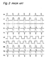
- Fig. 1 and Fig. 2 is a timing chart illustrating waveforms of various signals in the circuit shown in Fig. 1.
- the waveform shaper 11 of the PLL circuit 1 shapes the received input horizontal synchronous signal HI to output the horizontal synchronous pulse H having a constant pulse width, which is supplied to the phase detector 12 and the frequency-to-voltage converter 21.
- the phase detector 12 compares the phase of the horizontal synchronous pulse H and the phase of the oscillation signal VF which is the output of the PLL circuit 1, and outputs the phase difference signal P1.
- the low pass filter 13 integrates the phase difference signal P1 and outputs the current signal F1.
- the tracking control signal IF is at a constant value, and therefore, the current adder 14 adds the tracking control signal IF of the constant value and the current signal F1, to generate the control signal C.
- the current controlled oscillator 15 oscillates and generates the oscillation signal VF having the frequency corresponding to the current value of the control signal C.
- This oscillation signal VF is supplied to the phase detector 12 and the phase shifter 31 and the phase detector 33 of the output circuit 3.
- the PLL circuit 1 operates to the effect that the phase difference signal P1 outputted from the phase detector 12 becomes zero, namely, the frequency of the oscillation signal VF generated by the current controlled oscillator 5 becomes coincident with the frequency of the horizontal synchronous signal HI.
- the frequency-to-voltage converter 21 of the tracing circuit 2 converts the frequency of the received horizontal synchronous pulse H into the voltage signal VH, which is supplied to the low pass filter 22.
- the low pass filter 22 eliminates a high frequency component such as noises and others, included in the voltage signal VH, and integrates the voltage signal VH to generate the integration signal F2 to the voltage-to-current converter 25.
- the voltage-to-current converter 25 converts the integration signal F2 into a current value and generates the tracking control signal IF having the current value in proportion to the frequency of the horizontal synchronous pulse H.
- the mimimum oscillation frequency voltage supply 23 generates the minimum voltage signal FL for setting the frequency of the current controlled oscillator 15 to a constant value, in this case, to a minimum value which is equal to or lower than a lowest frequency of a normal operation, when no horizontal synchronous pulse H is supplied.
- the minimum voltage signal FL is supplied through the clipping diode 24 to the voltage-to-current converter 25.
- the tracking circuit 2 when the PLL circuit 1 is unlocked to be brought into an unlocked condition because of a frequency change of the input horizontal synchronous signal H1 or another reason, the tracking circuit 2 generates the tracking control signal IF in proportion to the frequency of the horizontal synchronous pulse H.
- the tracking control signal IF is supplied to the current adder 14.
- the current adder 14 In the unlocked condition, since the phase difference signal P1, namely, the integration signal F1, is almost zero, the current adder 14 outputs the tracking control signal IF as it is, as the control signal C to the current controlled oscillator 15. Accordingly, the current controlled oscillator 15 operates in an open loop control mode of setting the oscillation frequency under control of the tracking control signal IF, and generates the oscillation signal VF. If the oscillation signal VF becomes almost the frequency of the horizontal synchronous pulse H and enters in the capture range of the PLL circuit 1, the PLL circuit 1 is put in the locked condition as mentioned above.
- the integration signal F2 becomes zero, so that the diode 24 becomes conductive, and therefore, the voltage signal FL generated in the voltage supply 23 is supplied through the diode 24 to the voltage-to-current converter 25.
- the voltage-to-current converter 25 outputs the tracking control signal IF corresponding to the voltage signal FL.
- the current controlled oscillator 15 operates in a free running oscillation in an open loop control mode of setting the oscillation frequency under control of the tracking control signal IF corresponding to the voltage signal FL, and generates the oscillation signal VF of the minimum oscillation frequency.
- the phase detector 33 in the output circuit 3 detects a phase difference between the oscillation signal VF and the blanking pulse PB outputted from the output amplifier 32, to output the phase difference signal P2.
- the low pass filter 34 integrates the phase difference signal P2 to output the control signal F3.
- the phase shifter 31 is controlled by the control signal F3 to shift the phase of the oscillation signal VF supplied from the PLL circuit 1, by a constant amount, and to output the phase-shifted signal PS to the output amplifier 32.
- This output amplifier 32 outputs the horizontal output signal HO which is a deflecting current signal for a deflecting coil (not shown), so that a cathode ray tube (CRT) which is a display means, is horizontally scanned.
- the output amplifier 32 outputs the blanking pulse PB which is obtained by delaying the horizontal output signal HO by a predetermined period and which corresponds to a blanking period in the horizontal scanning.
- the blanking pulse PB is supplied to the phase detector 33.
- the tracking circuit 2 performs the frequency tracking control of the current controlled oscillator 15 by the tracking control signal which is generated by frequency-to-voltage-converting the horizontal synchronous pulse H having the constant pulse width obtained by use of the waveform shaper 11.
- the tracking control signal which is generated by frequency-to-voltage-converting the horizontal synchronous pulse H having the constant pulse width obtained by use of the waveform shaper 11.
- the frequency conversion error in the blanking period is suppressed by integrating the voltage signal VH by the low pass filter 22 constructed to include a large capacitance capacitor and therefore to have a large time constant.
- the low pass filter 22 is constructed to include a large capacitance capacitor and therefore to have a large time constant in order to prevent the image distortion attributable to missing of the horizontal synchronous signal in the blanking period, a frequency change tracking capability becomes low when the frequency of the horizontal synchronous signal is changed. As a result, in a certain period just after the change of the horizontal synchronous signal frequency, a horizontal size varies in the display screen.
- the free running oscillation frequency is set by the constant voltage supplied through the clipping diode to the output side of the low pass filter of the tracking circuit.
- this constant voltage is required to be set lower than the voltage of the integration signal which is outputted from the low pass filter and which corresponds to the lowest frequency in the normal operation, in order to prevent the constant voltage from reversely flowing. Accordingly, it is a matter of course that the free running oscillation frequency is not greater than the lowest frequency mentioned above.
- Another object of the present invention is to provide a video display apparatus having a phase-locked loop, having an improved property of tracking the horizontal synchronous signal frequency, so that even just after change of the horizontal synchronous signal frequency, the horizontal synchronous signal frequency is quickly tracked, thereby to realize a stable image display having no horizontal size variation or fluctuation.
- Still another object of the present invention is to provide a video display apparatus having a phase-locked loop, capable of freely setting the free running oscillation frequency.
- a video display apparatus comprising a phase-locked loop receiving a horizontal synchronous signal for generating an oscillation signal following the frequency of the horizontal synchronous signal, a tracking circuit for generating a tracking control signal for moving a frequency of the oscillation signal into a predetermined capture range of the phase-locked loop when the frequency of the horizontal synchronous signal changes, so that the frequency of the oscillation signal follows the frequency of the horizontal synchronous signal, and an output circuit receiving and amplifying the oscillation signal to output a horizontal output signal, the tracking circuit including a switch circuit receiving the horizontal synchronous signal and the oscillation signal to supply the horizontal synchronous signal as a selected signal to the tracking circuit when the phase-locked loop is in an unlocked condition, and to supply the oscillation signal as the selected signal to the tracking circuit when the phase-locked loop is in a locked condition.
- FIG. 3 there is shown a block diagram illustrating a first embodiment of the video display apparatus in accordance with the present invention, using the PLL circuit.
- elements similar to those shown in Fig. 1 are given the same Reference Numerals, and explanation thereof will be omitted.
- the embodiment of the video display apparatus shown in Fig. 3 comprises the PLL circuit 1 and the output circuit 3 similar to those of the prior art example, and a tracking circuit 2A which is provided in place of the tracking circuit 2 in the prior art example and which is configured to generate the tracking control signal IF by selectively receiving either the input horizontal synchronous signal HI or the oscillation signal VF in accordance with a synchronism detection signal indicating whether or not the PLL circuit is in a locked condition. Therefore, explanation of the PLL circuit 1 and the output circuit 3 will be omitted.
- the tracking circuit 2A comprises the frequency-to-voltage converter 21, the low pass filter 22, the clipping diode 24, and the voltage-to-current converter 25, similarly to the tracking circuit 2 in the prior art example.
- the tracking circuit 2A further comprises a synchronism detecting circuit 26 receiving the horizontal synchronous pulse H and the oscillation signal VF for generating a synchronism detection signal SD, a switch circuit 27 receiving the input horizontal synchronous signal HI and the oscillation signal VF and controlled by the synchronism detection signal SD to select one of the input horizontal synchronous signal HI and the oscillation signal VF so as to output a selected signal SH, a waveform shaper 28 receiving and shaping the selected signal SH to output a pulse signal TH having a constant pulse width, and a voltage supply 23A which is provided in place of the voltage supply 23 provided in the tracking circuit 2 in the prior art example, and which is so configured to output an arbitrary voltage FX.
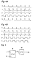
- Fig. 3 and Figs. 4A and 4B are timing charts showing waveforms of various signals in the circuit shown in Fig. 3, while particularly paying attention to portions different from the prior art example.
- the horizontal synchronous pulse H and the oscillation signal VF are supplied to the synchronism detecting circuit 26.
- the PLL circuit At a initial stage of application of the horizontal synchronous signal HI, the PLL circuit is in the unlocked condition in which the oscillation signal VF is not in synchronism with the horizontal synchronous signal HI, as shown in Fig. 4A. Therefore, the synchronism detecting circuit 26 outputs the synchronism detecting signal SD of a low level to the switch circuit 27, as will be described in detail later.
- the switch circuit 27 selects the horizontal synchronous signal HI and outputs the horizontal synchronous signal HI as the selected signal SH to the waveform shaper 28.
- the waveform shaper 28 shapes the selected signal SH into the pulse signal TH having the constant pulse width, which is supplied to the frequency-to-voltage converter 21
- the frequency-to-voltage converter 21 converts the frequency of the pulse signal TH into a voltage which is outputted as the signal VH.
- the signal VH is integrated by the low pass filter 22, and the voltage-to-current converter 25 outputs the tracking control signal IF, so that the current controlled oscillator 15 of the PLL circuit 1 is controlled. If the frequency of the oscillation signal VF ultimately approaches the frequency of the input horizontal synchronous signal HI and therefore enters in the capture range, the PLL circuit 1 is put into the locked condition, similarly to the prior art example. Thus, the oscillation signal VF is in synchronism with the horizontal synchronous signal HI.
- the synchronism detecting circuit 26 outputs the synchronism detecting signal SD of a high level to the switch circuit 27.
- the switch circuit 27 selects the oscillation signal VF and outputs the oscillation signal VF as the selected signal SH to the waveform shaper 28.
- the synchronism detecting circuit 26 includes a D-type flipflop 261 having a data input D connected to receive the horizontal synchronous pulse H and the clock input CK connected to receive the oscillation signal VF, and a latch circuit 262 receiving and latching a Q output of the flipflop 261 for outputting the latched signal as the synchronism detecting signal SD.
- Fig. 4A shows the unlocked condition of the PLL circuit 1
- Fig. 4B shows the locked condition of the PLL circuit 1.
- the high level period of the horizontal synchronous pulse H is coincident with the rising edge of the oscillation signal VF. Therefore, the Q output of the flipflop 261 is brought to the high level, and therefore, the latch circuit 262 latches the high level and outputs the synchronism detecting signal SD of the high level.
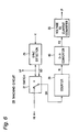
- FIG. 6 there is shown a block diagram of a modification of the tracking circuit in the circuit shown in Fig. 3.
- This modified tracking circuit is generally designated with Reference Numeral 2B.
- elements similar to those shown in Fig. 3 are given the same Reference Numerals, and explanation thereof will be omitted for simplification of description.
- the tracking circuit 2B includes, in place of the frequency-to-voltage converter 21, a counter 29 counting the selected signal SH for outputting a count value N, and a D/A (digital-to-analog) converter 40 for digital-to-analog-converting the count value N to a signal F2 which corresponds to the integrated signal F2 in the first embodiment.
- a D/A (digital-to-analog) converter 40 for digital-to-analog-converting the count value N to a signal F2 which corresponds to the integrated signal F2 in the first embodiment.
- the 20 pulses are because two vertical blanking periods are included in the period of 20 ms, and therefore, 20 horizontal synchronous signals are missed.
- the counting reference signal In order to prevent the above mentioned counting error, it is necessary to set the counting reference signal shorter than the vertical synchronous signal period.
- the low pass filter 22, the voltage supply 23 or 23A and the diode 24 which were required in the prior art example and in the first embodiment, are no longer necessary.
- the reason for this is that, because the input horizontal synchronous signal frequency is converted by use of the counter, it is no longer necessary to remove a high frequency component and to integrate the converted voltage by use of the low pass filter, and the free running oscillation control voltage corresponding to the minimum oscillation frequency can be set by an initial value of the counter.
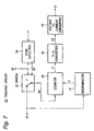
- FIG. 7 there is shown a block diagram of another modification of the tracking circuit in the circuit shown in Fig. 3.
- This modified tracking circuit is generally designated with Reference Numeral 2C.
- elements similar to those shown in Fig. 6 are given the same Reference Numerals, and explanation thereof will be omitted for simplification of description.
- the second modified tracking circuit 2C includes, in addition to the first modified tracking circuit 2B, a discriminator 41 receiving the input horizontal synchronous signal HI for discriminating presence/absence of the horizontal synchronous signal HI to generate a presence/absence discriminating signal U, which is supplied to the counter 29 as a control signal.
- Figs. 3 and 7 and Fig. 8 is a timing chart for illustrating an operation of the circuit shown in Fig. 3 incorporating the circuit shown in Fig. 7.
- the presence/absence discriminating signal U is brought to the high level, so that the counter 29 counts the horizontal synchronous pulse H, and the D/A converter 40 outputs the corresponding voltage signal F2, similarly to the first modified tracking circuit 2B.
- the discriminator 41 detects the absence of the horizontal synchronous signal HI and brings the presence/absence discriminating signal U to the low level, to cause the counter 29 to output a constant count value corresponding to the free running oscillation.
- the output signal F2 of the D/A converter 40 changes to the voltage corresponding to the free running oscillation.
- the current controlled oscillator 15 of the PLL circuit 1 generates the oscillation signal VF having the free running oscillation frequency.
- this free running oscillation frequency can be freely set by arbitrarily setting the above mentioned constant count value of the counter 29.
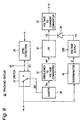
- FIG. 9 there is shown a block diagram of still another modification of the tracking circuit in the circuit shown in Fig. 3.
- This modified tracking circuit is generally designated with Reference Numeral 2D.
- elements similar to those shown in Figs. 3 and 7 are given the same Reference Numerals, and explanation thereof will be omitted for simplification of description.
- the third modified tracking circuit 2D is characterized in that the discriminator 41 is added to the tracking circuit 2A shown in Fig. 3.
- the presence/absence discriminating signal U outputted from the discriminator 41 is supplied to a voltage supply 23B, so that the voltage supply 23B is selectively put either into an operating condition when the presence/absence discriminating signal U is at the low level, or into a non-operating condition when the presence/absence discriminating signal U is at a high level. Therefore, since the voltage supply 23B operates only when no horizontal synchronous signal H1 is applied, it is possible to freely set the voltage value of the free running oscillation voltage signal FX outputted from the voltage supply 23B. Therefore, it is possible to freely set the free running oscillation frequency of the oscillation signal VF.
- the cracking circuit includes the switch circuit for selecting the horizontal synchronous signal to supply the horizontal synchronous signal to the tracking circuit when the phase-locked loop is in an unlocked condition, and for selecting tile oscillation signal of the phase-locked loop to supply the oscillation signal to the tracking circuit when the phase-locked loop is in a locked condition.
Landscapes
- Engineering & Computer Science (AREA)
- Multimedia (AREA)
- Signal Processing (AREA)
- Synchronizing For Television (AREA)
- Stabilization Of Oscillater, Synchronisation, Frequency Synthesizers (AREA)
- Controls And Circuits For Display Device (AREA)
Applications Claiming Priority (3)
| Application Number | Priority Date | Filing Date | Title |
|---|---|---|---|
| JP31759496 | 1996-11-28 | ||
| JP317594/96 | 1996-11-28 | ||
| JP8317594A JP2954052B2 (ja) | 1996-11-28 | 1996-11-28 | 映像表示装置 |
Publications (3)
| Publication Number | Publication Date |
|---|---|
| EP0845899A2 true EP0845899A2 (de) | 1998-06-03 |
| EP0845899A3 EP0845899A3 (de) | 2000-12-27 |
| EP0845899B1 EP0845899B1 (de) | 2004-03-03 |
Family
ID=18089969
Family Applications (1)
| Application Number | Title | Priority Date | Filing Date |
|---|---|---|---|
| EP97120849A Expired - Lifetime EP0845899B1 (de) | 1996-11-28 | 1997-11-27 | Videowiedergabegerät mit Phasenregelschleife zur Synchronisierung der horizontaler Abtastfrequenz mit der Synchroneingangssignalfrequenz |
Country Status (5)
| Country | Link |
|---|---|
| US (1) | US6014177A (de) |
| EP (1) | EP0845899B1 (de) |
| JP (1) | JP2954052B2 (de) |
| KR (1) | KR100265503B1 (de) |
| DE (1) | DE69727889T2 (de) |
Families Citing this family (19)
| Publication number | Priority date | Publication date | Assignee | Title |
|---|---|---|---|---|
| JPH1124030A (ja) * | 1997-06-30 | 1999-01-29 | Sony Corp | 液晶駆動装置 |
| US6177959B1 (en) * | 1997-12-31 | 2001-01-23 | Telecruz Technology, Inc. | Circuit and method for generating a clock signal synchronized with time reference signals associated with television signals |
| KR100265710B1 (ko) * | 1998-02-06 | 2000-09-15 | 윤종용 | 자동 트랙킹 조정 기능을 갖는 평판 디스플레이장치 |
| KR100259265B1 (ko) * | 1998-02-09 | 2000-06-15 | 윤종용 | 자동 코오스 조정 기능을 갖는 평판 디스플레이 장치 |
| KR100287867B1 (ko) * | 1998-12-31 | 2001-05-02 | 구자홍 | 디지털 텔레비전의 타이밍 복원 장치 |
| US6438188B1 (en) * | 1999-01-11 | 2002-08-20 | Alcatel Usa Sourcing, L.P. | Method and apparatus for a digitally controlled constant current source for phase adjustment of a synthesized clock |
| JP3367465B2 (ja) | 1999-05-13 | 2003-01-14 | 日本電気株式会社 | 発振周波数調整装置 |
| US6275072B1 (en) * | 1999-10-07 | 2001-08-14 | Velio Communications, Inc. | Combined phase comparator and charge pump circuit |
| US6160861A (en) * | 1999-10-22 | 2000-12-12 | Motorola, Inc. | Method and apparatus for a frequency modulation phase locked loop |
| US6674772B1 (en) * | 1999-10-28 | 2004-01-06 | Velio Communicaitons, Inc. | Data communications circuit with multi-stage multiplexing |
| US6952431B1 (en) | 1999-10-28 | 2005-10-04 | Rambus Inc. | Clock multiplying delay-locked loop for data communications |
| KR100365497B1 (ko) * | 2000-12-15 | 2002-12-18 | 엘지.필립스 엘시디 주식회사 | 액정표시장치 및 그 구동방법 |
| US7197659B2 (en) * | 2001-09-28 | 2007-03-27 | Intel Corporation | Global I/O timing adjustment using calibrated delay elements |
| US6856358B1 (en) * | 2002-01-16 | 2005-02-15 | Etron Technology, Inc. | Phase-increase induced backporch decrease (PIBD) phase recovery method for video signal processing |
| JP4379380B2 (ja) * | 2005-04-28 | 2009-12-09 | ソニー株式会社 | 水平レジスタ転送パルス生成回路及び撮像装置 |
| US9584139B2 (en) * | 2014-09-24 | 2017-02-28 | Intel IP Corporation | Phase tracker for a phase locked loop |
| CN107769772B (zh) * | 2017-11-02 | 2023-09-01 | 中国科学院西安光学精密机械研究所 | 一种低晃动同步扫描电路系统 |
| CN115941856B (zh) * | 2022-11-18 | 2025-08-26 | 海宁奕斯伟计算技术有限公司 | 数据流时钟信号的生成电路、方法、电子设备及存储介质 |
| CN120710499A (zh) * | 2024-03-25 | 2025-09-26 | 联发科技(新加坡)私人有限公司 | 锁相环电路 |
Family Cites Families (12)
| Publication number | Priority date | Publication date | Assignee | Title |
|---|---|---|---|---|
| JPS5586212A (en) * | 1978-12-22 | 1980-06-28 | Sony Corp | Frequency tracking circuit |
| JPS59164918U (ja) * | 1983-04-21 | 1984-11-05 | ソニー株式会社 | ビデオ信号及びデイジタル信号の再生装置 |
| US4660080A (en) * | 1985-12-24 | 1987-04-21 | Rca Corporation | Synchronization circuit responsive to time-multiplexed signals |
| US4634939A (en) * | 1985-12-24 | 1987-01-06 | Rca Corporation | Circuit synchronized by a signal at a deflection frequency |
| DE68915228T2 (de) * | 1988-09-02 | 1994-12-15 | Sanyo Electric Co | Phasensynchronisierschaltung in einem Videosignalempfänger und Verfahren zur Herstellung der Phasensynchronisation. |
| US4933959A (en) * | 1989-05-08 | 1990-06-12 | Datatape Incorporated | Tracking bit synchronizer |
| JPH02309778A (ja) * | 1989-05-24 | 1990-12-25 | Victor Co Of Japan Ltd | クロック生成回路 |
| JPH05207327A (ja) * | 1992-01-27 | 1993-08-13 | Mitsubishi Electric Corp | 水平同期回路 |
| US5381116A (en) * | 1993-12-13 | 1995-01-10 | Motorola, Inc. | Method and apparatus for performing frequency tracking in an all digital phase lock loop |
| JPH07199891A (ja) * | 1993-12-28 | 1995-08-04 | Canon Inc | 表示制御装置 |
| US5825431A (en) * | 1996-12-18 | 1998-10-20 | Eastman Kodak Company | H-sync to pixel clock phase detection circuit |
| US5889500A (en) * | 1997-01-31 | 1999-03-30 | Dynacolor Inc. | Single chip display system processor for CRT based display systems |
-
1996
- 1996-11-28 JP JP8317594A patent/JP2954052B2/ja not_active Expired - Fee Related
-
1997
- 1997-11-26 US US08/979,699 patent/US6014177A/en not_active Expired - Fee Related
- 1997-11-27 EP EP97120849A patent/EP0845899B1/de not_active Expired - Lifetime
- 1997-11-27 DE DE69727889T patent/DE69727889T2/de not_active Expired - Fee Related
- 1997-11-28 KR KR1019970063872A patent/KR100265503B1/ko not_active Expired - Fee Related
Also Published As
| Publication number | Publication date |
|---|---|
| EP0845899B1 (de) | 2004-03-03 |
| KR100265503B1 (ko) | 2000-09-15 |
| EP0845899A3 (de) | 2000-12-27 |
| DE69727889D1 (de) | 2004-04-08 |
| DE69727889T2 (de) | 2004-07-29 |
| JPH10164395A (ja) | 1998-06-19 |
| KR19980042889A (ko) | 1998-08-17 |
| JP2954052B2 (ja) | 1999-09-27 |
| US6014177A (en) | 2000-01-11 |
Similar Documents
| Publication | Publication Date | Title |
|---|---|---|
| EP0845899B1 (de) | Videowiedergabegerät mit Phasenregelschleife zur Synchronisierung der horizontaler Abtastfrequenz mit der Synchroneingangssignalfrequenz | |
| KR19990069420A (ko) | 자동 코오스 조정 기능을 갖는 평판 디스플레이 장치 | |
| EP0461897B1 (de) | Schaltung zur Trennung eines horizontalen Synchronisierungssignals für ein Anzeigegerät | |
| JP2583406B2 (ja) | 映像表示装置 | |
| JP2610726B2 (ja) | 同期信号復元回路 | |
| JP2010200383A (ja) | 水平周波数信号発生器、同期回路、およびビデオ表示装置 | |
| JPS62159981A (ja) | ビデオ装置用同期回路 | |
| JP2511843B2 (ja) | タイミング信号発生回路 | |
| KR100673912B1 (ko) | 수평 주파수 발생 장치 | |
| JPS60134564A (ja) | 水平afc回路 | |
| JPS58707B2 (ja) | 垂直同期信号検出方法および回路 | |
| KR100730006B1 (ko) | 수평 주파수 선택의 제어 장치 | |
| EP0472326B1 (de) | Schaltung zur Trennung eines horizontalen Synchronisierungssignals | |
| KR100363098B1 (ko) | 비디오 카세트 레코더(vcr) 신호 검출장치 및 방법 | |
| JPH07283731A (ja) | 同期信号回路 | |
| JP4757690B2 (ja) | Pllシステム及び車載用テレビジョンシステム | |
| JP2696910B2 (ja) | 水平同期回路 | |
| JPH08251445A (ja) | 弱電界検出回路 | |
| JPH10285427A (ja) | 垂直同期回路 | |
| JPH04263293A (ja) | 水平周波数判別回路 | |
| JP3473713B2 (ja) | ブランキングパルス作成回路 | |
| KR910009486Y1 (ko) | 수직동기 분리 및 동기 검파회로 | |
| KR920001109B1 (ko) | Vdp정지신호 검출회로 | |
| JPH08149329A (ja) | ビデオ信号検出装置 | |
| JP2000138842A (ja) | 垂直同期検出回路 |
Legal Events
| Date | Code | Title | Description |
|---|---|---|---|
| PUAI | Public reference made under article 153(3) epc to a published international application that has entered the european phase |
Free format text: ORIGINAL CODE: 0009012 |
|
| AK | Designated contracting states |
Kind code of ref document: A2 Designated state(s): DE GB |
|
| AX | Request for extension of the european patent |
Free format text: AL;LT;LV;MK;RO;SI |
|
| PUAL | Search report despatched |
Free format text: ORIGINAL CODE: 0009013 |
|
| AK | Designated contracting states |
Kind code of ref document: A3 Designated state(s): AT BE CH DE DK ES FI FR GB GR IE IT LI LU MC NL PT SE |
|
| AX | Request for extension of the european patent |
Free format text: AL;LT;LV;MK;RO;SI |
|
| 17P | Request for examination filed |
Effective date: 20001120 |
|
| 17Q | First examination report despatched |
Effective date: 20010323 |
|
| AKX | Designation fees paid |
Free format text: DE GB |
|
| GRAH | Despatch of communication of intention to grant a patent |
Free format text: ORIGINAL CODE: EPIDOS IGRA |
|
| RAP1 | Party data changed (applicant data changed or rights of an application transferred) |
Owner name: NEC ELECTRONICS CORPORATION |
|
| GRAS | Grant fee paid |
Free format text: ORIGINAL CODE: EPIDOSNIGR3 |
|
| GRAA | (expected) grant |
Free format text: ORIGINAL CODE: 0009210 |
|
| AK | Designated contracting states |
Kind code of ref document: B1 Designated state(s): DE GB |
|
| REG | Reference to a national code |
Ref country code: GB Ref legal event code: FG4D |
|
| REF | Corresponds to: |
Ref document number: 69727889 Country of ref document: DE Date of ref document: 20040408 Kind code of ref document: P |
|
| PLBE | No opposition filed within time limit |
Free format text: ORIGINAL CODE: 0009261 |
|
| STAA | Information on the status of an ep patent application or granted ep patent |
Free format text: STATUS: NO OPPOSITION FILED WITHIN TIME LIMIT |
|
| 26N | No opposition filed |
Effective date: 20041206 |
|
| PGFP | Annual fee paid to national office [announced via postgrant information from national office to epo] |
Ref country code: DE Payment date: 20081120 Year of fee payment: 12 |
|
| PGFP | Annual fee paid to national office [announced via postgrant information from national office to epo] |
Ref country code: GB Payment date: 20081126 Year of fee payment: 12 |
|
| GBPC | Gb: european patent ceased through non-payment of renewal fee |
Effective date: 20091127 |
|
| PG25 | Lapsed in a contracting state [announced via postgrant information from national office to epo] |
Ref country code: DE Free format text: LAPSE BECAUSE OF NON-PAYMENT OF DUE FEES Effective date: 20100601 |
|
| PG25 | Lapsed in a contracting state [announced via postgrant information from national office to epo] |
Ref country code: GB Free format text: LAPSE BECAUSE OF NON-PAYMENT OF DUE FEES Effective date: 20091127 |