EP0848298A2 - Appareil d'exposition et procédés l'utilisant - Google Patents
Appareil d'exposition et procédés l'utilisant Download PDFInfo
- Publication number
- EP0848298A2 EP0848298A2 EP97122087A EP97122087A EP0848298A2 EP 0848298 A2 EP0848298 A2 EP 0848298A2 EP 97122087 A EP97122087 A EP 97122087A EP 97122087 A EP97122087 A EP 97122087A EP 0848298 A2 EP0848298 A2 EP 0848298A2
- Authority
- EP
- European Patent Office
- Prior art keywords
- light
- light source
- supported
- optical system
- exposure apparatus
- Prior art date
- Legal status (The legal status is an assumption and is not a legal conclusion. Google has not performed a legal analysis and makes no representation as to the accuracy of the status listed.)
- Withdrawn
Links
Images



Classifications
-
- G—PHYSICS
- G03—PHOTOGRAPHY; CINEMATOGRAPHY; ANALOGOUS TECHNIQUES USING WAVES OTHER THAN OPTICAL WAVES; ELECTROGRAPHY; HOLOGRAPHY
- G03F—PHOTOMECHANICAL PRODUCTION OF TEXTURED OR PATTERNED SURFACES, e.g. FOR PRINTING, FOR PROCESSING OF SEMICONDUCTOR DEVICES; MATERIALS THEREFOR; ORIGINALS THEREFOR; APPARATUS SPECIALLY ADAPTED THEREFOR
- G03F7/00—Photomechanical, e.g. photolithographic, production of textured or patterned surfaces, e.g. printing surfaces; Materials therefor, e.g. comprising photoresists; Apparatus specially adapted therefor
- G03F7/70—Microphotolithographic exposure; Apparatus therefor
- G03F7/70058—Mask illumination systems
-
- G—PHYSICS
- G03—PHOTOGRAPHY; CINEMATOGRAPHY; ANALOGOUS TECHNIQUES USING WAVES OTHER THAN OPTICAL WAVES; ELECTROGRAPHY; HOLOGRAPHY
- G03F—PHOTOMECHANICAL PRODUCTION OF TEXTURED OR PATTERNED SURFACES, e.g. FOR PRINTING, FOR PROCESSING OF SEMICONDUCTOR DEVICES; MATERIALS THEREFOR; ORIGINALS THEREFOR; APPARATUS SPECIALLY ADAPTED THEREFOR
- G03F7/00—Photomechanical, e.g. photolithographic, production of textured or patterned surfaces, e.g. printing surfaces; Materials therefor, e.g. comprising photoresists; Apparatus specially adapted therefor
- G03F7/70—Microphotolithographic exposure; Apparatus therefor
- G03F7/70216—Mask projection systems
- G03F7/70258—Projection system adjustments, e.g. adjustments during exposure or alignment during assembly of projection system
-
- G—PHYSICS
- G03—PHOTOGRAPHY; CINEMATOGRAPHY; ANALOGOUS TECHNIQUES USING WAVES OTHER THAN OPTICAL WAVES; ELECTROGRAPHY; HOLOGRAPHY
- G03F—PHOTOMECHANICAL PRODUCTION OF TEXTURED OR PATTERNED SURFACES, e.g. FOR PRINTING, FOR PROCESSING OF SEMICONDUCTOR DEVICES; MATERIALS THEREFOR; ORIGINALS THEREFOR; APPARATUS SPECIALLY ADAPTED THEREFOR
- G03F7/00—Photomechanical, e.g. photolithographic, production of textured or patterned surfaces, e.g. printing surfaces; Materials therefor, e.g. comprising photoresists; Apparatus specially adapted therefor
- G03F7/70—Microphotolithographic exposure; Apparatus therefor
- G03F7/708—Construction of apparatus, e.g. environment aspects, hygiene aspects or materials
- G03F7/70808—Construction details, e.g. housing, load-lock, seals or windows for passing light in or out of apparatus
- G03F7/70833—Mounting of optical systems, e.g. mounting of illumination system, projection system or stage systems on base-plate or ground
Definitions
- the present invention concerns projection-exposure apparatus and methods employing a projection-exposure apparatus for manufacturing semiconductor devices, and in particular such apparatus and methods employing an excimer laser light source.
- Projection-exposure apparatus for manufacturing semiconductor elements, liquid crystal display elements, and the like tend to be large and bulky, and require a large area of floor space for their installation.
- Such exposure apparatus generally employ mercury lamps, laser light sources, or the like as light sources.
- Laser light sources, particularly excimer laser light sources are extremely large compared to light sources such as mercury lamps. Accordingly, particularly with exposure apparatus employing excimer laser light sources, it is necessary to arrange the light source separately from the exposure apparatus main assembly. To allow effective utilization of clean room floor space, the excimer laser light source is sometimes installed on a floor level beneath the floor of the clean room housing the exposure apparatus. Such lower rooms frequently have a lower cleanliness rating.
- a projection-exposure apparatus typically employs an optical integrator to uniformly illuminate the mask.
- the optical integrator must be illuminated with high efficiency by light from the light source.
- floor deformation and displacement of one floor level relative to the other floor level can cause misalignment of the light beam that illuminates the optical integrator.
- misalignment results in reduced illuminance and reduced uniformity of the illuminance profile at the photosensitive substrate (i.e., the surface being exposed).
- an excimer laser light source and an associated exposure apparatus main assembly are sometimes secured to a "grating" or the like installed some distance above a common floor, wherein a space located between the floor and the grating are utilized for plumbing and other utilities.
- deformation or other displacement of the grating which tends to be more easily deformed than a floor, can cause misalignment of the light beam that illuminates the optical integrator, resulting in reduced illuminance, and reduced uniformity of the illuminance profile, at the photosensitive substrate. It is desirable to avoid such deleterious effects.
- Effective utilization of any space between the excimer laser light source and the exposure apparatus main assembly (supported on a grating by the same floor system) is also desirable.
- the present invention provides, inter alia , a projection-exposure apparatus in which, even when the light source apparatus and the exposure apparatus main assembly are supported by different structural bodies in a building, the illuminance profile at the surface being exposed is not easily affected by deformation or relative displacement of the respective structural bodies.
- the present invention also encompasses methods for manufacturing, using such projection-exposure apparatus, a semiconductor device or other device requiring projection exposure during manufacture.
- the present invention further provides exposure apparatus wherein, even when the light source apparatus and the exposure apparatus main assembly are supported by the same structural body by way of, for example, a grating, the illuminance profile at the surface being exposed is not easily affected by deformation or the like of the grating or structural body, and wherein effective utilization of the space between the light-source apparatus and the exposure apparatus main assembly is facilitated.
- the present invention also encompasses methods for manufacturing a semiconductor device employing such an exposure apparatus.
- An exposure apparatus comprises a light source to be supported by a first structural body, an illumination optical system to be supported by a second structural body that is substantially isolated from the first structural body, a first light-collecting system supported by the first structural body and for condensing light from the light source, and a second light-collecting system supported by the second structural body and for guiding, to the illumination optical system, light that has been condensed by the first light-collecting system.
- the illumination optical system comprises, at its incident side, a surface or plane that is conjugate to the mask or mask plane. The surface and the exit plane of the light source are rendered substantially optically conjugate relative to each other by the first light-collecting system and the second light-collecting system, so that a prescribed pattern formed on a mask may be reliably and uniformly illuminated.
- the illumination optical system comprises an optical integrator for forming multiple light-source images using light from the second light-collecting system, and a condenser optical system that condenses light from the multiple light-source images formed by the optical integrator for illuminating the mask.
- the optical integrator is then arranged such that its entrance plane essentially coincides with the surface.
- the light source preferably comprises an excimer laser light source.
- the first light-collecting system condenses a collimated light beam from the excimer laser light source, and the second light-collecting system recollimates the light beam that was first condensed by the first light-collecting system.
- an exposure apparatus comprises a first light-collecting system that condenses a light beam from a light source and a second light-collecting system that guides, to an illumination optical system, the light beam that has been condensed by the first light-collecting system.
- a first support body supports the first light-collecting system and a second support body, independent of the first support body, supports the second light-collecting system.
- the first and second light collecting systems are preferably arranged such that an exit plane of the light source is optically conjugate to an entrance plane of the illumination optical system, which in turn is optically conjugate to a mask plane at which a mask is to be illuminated.
- the illumination optical system preferably comprises an optical integrator, and the entrance plane of the illumination optical system is preferably located at the entrance plane of the optical integrator.
- the present invention also encompasses methods for manufacturing a semiconductor device employing an exposure apparatus according to the present invention, so as to achieve improved exposure of a photosensitive substrate.
- Embodiments of the present invention are not limited to the structures and configurations as summarized above. Further objects and advantages of the present invention will be apparent to those of ordinary skill in the art from the following description, which proceeds with reference to the accompanying figures, by way of non-limiting exemplary embodiments of the present invention.
- FIG. 1 is a schematic diagram of a first example embodiment of a projection-exposure apparatus according to the present invention.
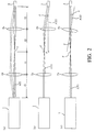
- FIGS. 2(a)-2(c) are schematic diagrams of an optical path from the excimer laser light source 1 to the optical integrator 3 of FIG. 1, illustrating some effects of the present invention.
- FIG. 3 is a schematic diagram of the exposure apparatus of FIG. 1, wherein the upper-level floor system A of FIG. 1 is displaced with respect to the lower-level floor system B in a horizontal direction by a prescribed amount d.
- FIG. 4 is a schematic diagram of the exposure apparatus of FIG. 1, wherein the upper-level floor system A of FIG. 1 is deformed so as to become convex, as viewed from below, due to the weight of the exposure apparatus main assembly or the like.
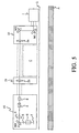
- FIG. 5 is a schematic diagram of a second embodiment of a projection-exposure apparatus according to the present invention.
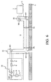
- FIG. 6 is a schematic diagram of a third embodiment of a projection-exposure apparatus according to the present invention.
- a first light-collecting system and a second light-collecting system constitute a relay optical system.
- the laser exit plane of a light source such as an excimer laser light source, and the entrance plane of an optical integrator are arranged so as to be optically conjugate to each other.
- the first light-collecting system can be supported, together with the excimer laser light source, by a first structural body.
- the second light-collecting system can be supported, together with the optical integrator, by a second structural body that is substantially isolated from the first structural body.
- the relay optical system operates such that the illuminance profile at the surface being exposed (e.g., photosensitive wafer) is essentially unaffected by deformation or displacement of the first and/or second structural bodies relative to each other.
- a projection-exposure apparatus according to the present invention produces a uniform illuminance profile at the surface being exposed, thereby allowing stable and satisfactory exposure to be performed. Accordingly, use of a projection-exposure apparatus according to the present invention facilitates production of a satisfactory semiconductor device.
- FIG. 1 is a schematic diagram showing certain features of a projection-exposure apparatus according to a first example embodiment of the present invention.
- a collimated light beam propagating in a horizontal direction in the figure from the excimer laser light source 1 is deflected in a vertical direction in the figure by a cornering mirror M1.
- the light beam is incident upon a first light-collecting lens 2a.
- the light beam is condensed by the first light-collecting lens 2a and recollimated by a second light-collecting lens 2b.
- the recollimated light beam is deflected in a horizontal direction in the figure by the cornering mirror M2, and is incident upon a beam expander 8 that comprises, for example, a pair of cylindrical lenses.
- the light beam is enlarged by the beam expander 8 in two dimensions in a plane perpendicular to the optical axis AX, so as to make the transverse dimensions of the light beam essentially the same as the transverse dimensions of the entrance plane of an optical integrator 3.
- the optical integrator 3 is preferably configured as a fly-eye lens, for example.
- the optical integrator 3 preferably comprises multiple lenses that separate and condense light passing therethrough into multiple light-source images at the back focus of the optical integrator. Light from the multiple light-source images are incident upon a condenser lens 4.
- the superimposed light-source images illuminate a mask 5 that defines a prescribed pattern for projection exposure.
- the light beam is transmitted though the mask 5 and through a projection optical system 6 to form an image of the mask pattern on a photosensitive wafer 7 (or other suitable photosensitive substrate).
- the mask 5 is mounted on a mask stage (not shown) in a plane perpendicular to the optical axis of the projection optical system 6.
- the wafer 7 is mounted on a wafer stage (not shown) that is preferably movable in two dimensions within a plane perpendicular to the optical axis of the projection optical system 6.
- Exposure is conducted while moving the wafer stage, and thus the wafer 7, relative to the projection optical system 6.
- the mask pattern is sequentially transferred to respective exposure regions on the wafer 7.
- the cornering mirror M1 and the first light-collecting lens 2a are supported by a support body 11.
- the excimer laser light source 1 and the support body 11 (and thus the cornering mirror M1 and the first light-collecting lens 2a) are supported by a lower-level floor system B, which serves as a first structural body.
- the cornering mirror M2 is supported by an exposure apparatus main assembly 10 that comprises the optical integrator 3.
- the second light-collecting lens 2b is supported by a support body 12.
- the exposure apparatus main assembly 10 and the support body 12 (and thus the second light-collecting lens 2b) are supported by an upper-level floor system A that serves as a second structural body.
- the second structural body is substantially isolated from the first structural body.
- Flexible conduits or the like extend between the excimer laser light source 1 and the support body 11, between the support body 11 and the support body 12, and between the exposure apparatus main assembly 10 and the support body 12, as indicated by the broken lines in FIG. 1.
- the flexible conduits prevent any light propagating therethrough from being affected by changes and air currents in the surrounding environment. (In FIGS. 3 and 4, described below, such flexible conduits are omitted for simplicity of illustration.)
- FIGS. 2(a)-2(c) depict the optical path from the excimer laser light source 1 to the optical integrator 3. (For simplicity, FIGS. 2(a)-2(c) do not show the cornering mirrors M1 and M2, or the beam expander 8.)
- a collimated light beam (indicated by solid lines in the drawing) propagating along the optical axis AX from the excimer laser light source 1 is incident upon the first light-collecting lens 2a (having a focal length f1).
- the first light-collecting lens 2a condenses the light beam onto a point F residing on the optical axis AX.
- the light beam is recollimated by the second light-collecting lens 2b (having a focal length f2).
- the re-collimated beam is then incident upon the optical integrator 3.
- the exit plane of the excimer laser light source 1 is situated at the front focal plane of the first light-collecting lens 2a.
- the entrance plane of the optical integrator 3 is situated at the back focal plane of the second light-collecting lens 2b.
- the first light-collecting lens 2a and the second light-collecting lens 2b are situated such that the exit plane of the excimer laser light source 1 and the entrance plane of optical integrator 3 are optically conjugate to each other.
- the collimated light beam (indicated by broken lines in FIG. 2(a)) emitted from the excimer laser light source 1 obliquely with respect to the optical axis AX reaches the entrance plane of the optical integrator 3 with no positional misalignment, despite any angular misalignment.
- the excimer laser light source 1 and the first light-collecting lens 2a are supported by the lower-level floor system B, and the second light-collecting lens 2b and the optical integrator 3 are supported by the upper-level floor system A. Accordingly, as shown in FIG. 3, if the upper-level floor system A is displaced with respect to the lower-level floor system B in a horizontal direction by an amount d, then the optical axis AX1 of the first light-collecting lens 2a and the optical axis AX2 of the second light-collecting lens 2b will be misaligned in a horizontal direction (in the figure) by an amount d. That is, in FIG.
- the optical axis AX1 of the first light-collecting lens 2a and the optical axis AX2 of the second light-collecting lens 2b will be misaligned in a vertical direction (in the figure) by the amount d.
- the focal length f2 of the second light-collecting lens 2b can be large compared to the relative displacement d of the floor systems, so any effect of the angular misalignment ⁇ on the illuminance profile at the surface being exposed is so small that the effect can be ignored.
- the optical axis AX2 of the second light-collecting lens 2b will become oblique by an angle ⁇ relative to the optical axis AX1 of the first light-collecting lens 2a. That is, as shown in FIG. 2(c) (showing the optical path in a situation such as that shown in FIG. 4), the optical axis AX2 of the second light-collecting lens 2b becomes oblique by the angle ⁇ relative to the optical axis AX1 of the first light-collecting lens 2a.
- FIG. 2(c) shown the optical path in a situation such as that shown in FIG. 4
- the light beam having passed through the second light-collecting lens 2b (which is slightly oblique with respect to the optical axis AX1), reaches the entrance plane of the optical integrator 3 with almost no angular misalignment or positional misalignment. Accordingly, any effect of obliqueness of the optical axis AX2 of the second light-collecting lens 2b on the illuminance profile at the surface being exposed is so small that the effect can be ignored.
- any effect on the illuminance profile at the surface being exposed is so small that the effect can be ignored.
- the first light-collecting lens 2a and the second light-collecting lens 2b constitute a relay lens system in which the exit plane of the excimer laser light source 1 and the entrance plane of the optical integrator 3 are substantially conjugate to each other.
- the first light-collecting lens 2a is supported by the floor system B integrally with the excimer laser light source 1
- the second light-collecting lens 2b is supported by the floor system B integrally with the optical integrator 3.
- the exposure apparatus of the first example embodiment permits stable and satisfactory exposures to be performed.
- FIG. 5 is a schematic diagram of a projection-exposure apparatus according to a second example embodiment of the present invention.
- the second example embodiment shares certain similarities with the first example embodiment. However, as explained below, the arrangement and manner by which certain structures in the second example embodiment are supported differ from the first example embodiment.
- components that are the same as in the first example embodiment are denoted using the same reference designators and are not described further.
- the collimated light beam supplied horizontally and to the left (in the figure) from an excimer laser light source 1, is deflected vertically upward (in the figure) by a cornering mirror M1.
- the light beam is then incident upon a cornering mirror M2 that deflects the light beam horizontally toward the left (in the figure) to be incident upon a first light-collecting lens 2a.
- the light-collecting lens 2a condenses the light beam which is subsequently recollimated by passage through a second light-collecting lens 2b.
- the recollimated light beam is incident upon a beam expander 8 within the exposure apparatus main assembly 10.
- the cornering mirror M1, the cornering mirror M2, and the first light-collecting lens 2a are all supported by a support body 20, and the second light-collecting lens 2b is supported by a support body 21 comprising a support structure that is independent of the support body 20.
- Flexible conduits preferably extend between the excimer laser light source 1 and the support body 20, between the support body 20 and the support body 21, and between the exposure apparatus main assembly 10 and the support body 21, as indicated by the broken lines in FIG. 5.
- the conduits prevent light propagating therethrough from being affected by external air currents and other changes in the external environment.
- the excimer laser light source 1, the support body 20 (and thus the cornering mirror M1, the cornering mirror M2, and the first light-collecting lens 2a), the support body 21 (and thus the second light-collecting lens 2b), and the exposure apparatus main assembly 10 are all supported by a structural body such as, for example, a grating G.
- the grating G is supported by a floor system A.
- the excimer laser light source 1, the first light-collecting lens 2a, the second light-collecting lens 2b, and the exposure apparatus main assembly 10 are all supported by the same structural body (i.e., the floor system A), by way of the grating G.
- the space between the grating G and the floor system A can be used for routing utilities.
- the first light-collecting lens 2a and the second light-collecting lens 2b of the second example embodiment constitute a relay lens system in which the exit plane of the excimer laser light source 1 and the entrance plane of the optical integrator 3 have a conjugate relationship with each other.
- the focal length of the first light-collecting lens 2a is denoted f1 and the focal length of the second light-collecting lens 2b is denoted f2
- the exit plane of the excimer laser light source 1 and the first light-collecting lens 2a are separated by a distance f1 along the optical axis
- the first light-collecting lens 2a and the second light-collecting lens 2b are separated by a distance (f1 + f2) along the optical axis
- the second light-collecting lens 2b and the entrance plane of the optical integrator 3 are separated by a distance f2 along the optical axis.
- the first light-collecting lens 2a and the second light-collecting lens 2b comprise a relay lens system in which the laser exit plane of the excimer laser light source 1 and the entrance plane of the optical integrator 3 have a conjugate relationship with each other, satisfactory illumination of the entrance plane of the optical integrator 3 is achieved. No positional misalignment arises despite any angular misalignment that might be experienced by the excimer laser light source 1. Also, the first light-collecting lens 2a is supported by the support body 20 (which is comparatively near the excimer laser light source 1) and the second light-collecting lens 2b is supported by the support body 21 (which is comparatively near the exposure apparatus main assembly 10).
- the action of the relay lens system permits a uniform illuminance profile to be obtained at the wafer 7.
- any underlying space C (indicated by broken lines in the figure) can be utilized as required for equipment and utilities, for example.
- FIG. 6 is a schematic diagram of an exposure apparatus according to a third example embodiment of the present invention.
- the third example embodiment shares certain similarities with the first and second example embodiments, except that the arrangement and manner by which certain components of the third example embodiment are supported differ from the first and second example embodiments.
- components that are the same as in the second example embodiment have the same reference designators and are not described further.
- the collimated light beam supplied horizontally toward the left (in the figure) from an excimer laser light source 1 is deflected vertically downward by a cornering mirror M1.
- the light beam is then incident upon a cornering mirror M2 which deflects the light beam horizontally toward the left (in the figure).
- the light beam is then incident upon a first light-collecting lens 2a which condenses the light beam.
- the light beam is recollimated by a second light-collecting lens 2b, and is then incident upon a cornering mirror M3.
- the recollimated light beam is deflected vertically upward (in the figure) by the cornering mirror M3, deflected horizontally toward the left (in the figure) by a cornering mirror M4, and is incident upon a beam expander 8 within an exposure apparatus main assembly 10.
- the first light-collecting lens 2a, the cornering mirror M1, and the cornering mirror M2 are supported by a support body 20.
- the second light-collecting lens 2b, the cornering mirror M3, and the cornering mirror M4 are supported by a support body 21 that comprises a support structure that is independent of the support body 20.
- Flexible conduits or the like preferably extend between the excimer laser light source 1 and the support body 20, between the support body 20 and the support body 21, and between the exposure apparatus main assembly 10 and the support body 21, as indicated by the broken lines in FIG. 6.
- the flexible conduits protect light propagating therethrough from the external environment and from air movement.
- the excimer laser light source 1 and the exposure apparatus main assembly 10 are supported by a structural body such as, for example, a grating G.
- the grating G, the support body 20 (and thus the cornering mirror M1, the cornering mirror M2, and the first light-collecting lens 2a), and the support body 21 (and thus the second light-collecting lens 2b, the cornering mirror M3, and the cornering mirror M4) are supported by the floor system A.
- the excimer laser light source 1, the exposure apparatus main assembly 10, the first light-collecting lens 2a, and the second light-collecting lens 2b are all ultimately supported by the same structural body (i.e., the floor system A).
- the excimer laser light source 1 and the exposure apparatus main assembly 10 are supported by the floor system A and the grating G.
- the first light-collecting lens 2a and the second light-collecting lens 2b are supported by the floor system A but not by the grating G.
- the first light-collecting lens 2a and the second light-collecting lens 2b comprise a relay lens system in which the exit plane of the excimer laser light source 1 and the entrance plane of the optical integrator 3 have a conjugate relationship with each other.
- the focal length of the first light-collecting lens 2a is denoted f1 and the focal length of the second light-collecting lens 2b is denoted f2
- the exit plane of the excimer laser light source 1 and the first light-collecting lens 2a are separated from each other by a distance f1 along the optical axis
- the first light-collecting lens 2a and the second light-collecting lens 2b are separated from each other by a distance (f1 + f2) along the optical axis
- the second light-collecting lens 2b and the entrance plane of the optical integrator 3 are separated from each other by a distance f2 along the optical axis.
- the first light-collecting lens 2a and the second light-collecting lens 2b comprise a relay lens system in which the exit plane of the excimer laser light source 1 and the entrance plane of the optical integrator 3 have a conjugate relationship to each other, satisfactory illumination of the entrance plane of the optical integrator 3 is achieved. Also, positional misalignment does not arise despite any angular misalignment that might be experienced by the excimer laser light source 1.
- the action of the relay lens system permits a uniform illuminance profile to be obtained at the wafer 7.
- the optical axis between the support body 20 and the support body 21 is situated below the grating G, the space D (defined by the support body 20, the support body 21, and the grating G) can be effectively utilized.
- the excimer laser light source 1, the first light-collecting lens 2a, the second light-collecting lens 2b, and the exposure apparatus main assembly 10 are all ultimately supported by the same structural body (i.e., the floor system A).
- the second example embodiment and the third example embodiment it is also possible to employ an arrangement similar to that of the first example embodiment, wherein the excimer laser light source 1 and the first light-collecting lens 2a are supported by a first structural body (e.g., a floor system A), and the second light-collecting lens 2b and the exposure apparatus main assembly 10 are supported by a second structural body (e.g., a separate floor system B) that is substantially isolated from the first structural body.
- a wafer that been photolithographically exposed using a projection-exposure apparatus according to the present invention is subsequently "developed”, etched (to remove material from regions not protected by the resist), “stripped” to remove residual resist after the etching step, and so forth, until wafer processing is completed.
- a semiconductor device such as an LSI is ultimately manufactured, by means of assembly operations such as a dicing operation wherein the wafer is cut into chips such that each such chip comprises one of the circuits exposed thereon, a bonding operation wherein each chip is provided with electrical leads and the like, and a packaging operation wherein each chip is separately packaged, and so forth.
- apparatus according to the present invention can alternatively comprise an ordinary light source.
- a beam expander 8 was situated on the optical axis between the relay lens system (lenses 2a and 2b) and the optical integrator 3.
- the beam expander 8 can be omitted by appropriately setting the ratio of the focal length f1 of the first light-collecting lens 2a to the focal length f2 of the second light-collecting lens 2b.
- the present invention can also be utilized for performing step-and-scan photolithographic exposures in which respective exposure regions of the wafer are scanned during exposure, i.e., both the wafer and mask move relative to the projection optical system during the exposure.
- the present invention can also be utilized for performing static-scan exposures in which the entire mask pattern is exposed onto the entire exposure region of a wafer in one exposure as the wafer and mask are moved relative to each other with respect to the projection optical system.
- optical integration can be achieved using an alternative component such as an internal-reflection-type rod-shaped optical integrator.
Landscapes
- Physics & Mathematics (AREA)
- General Physics & Mathematics (AREA)
- Health & Medical Sciences (AREA)
- Engineering & Computer Science (AREA)
- Environmental & Geological Engineering (AREA)
- Epidemiology (AREA)
- Public Health (AREA)
- Exposure Of Semiconductors, Excluding Electron Or Ion Beam Exposure (AREA)
- Exposure And Positioning Against Photoresist Photosensitive Materials (AREA)
Applications Claiming Priority (6)
| Application Number | Priority Date | Filing Date | Title |
|---|---|---|---|
| JP353022/96 | 1996-12-13 | ||
| JP35302296 | 1996-12-13 | ||
| JP35302296 | 1996-12-13 | ||
| JP307953/97 | 1997-10-22 | ||
| JP30795397 | 1997-10-22 | ||
| JP9307953A JPH10229044A (ja) | 1996-12-13 | 1997-10-22 | 露光装置および該露光装置を用いた半導体デバイスの製造方法 |
Publications (2)
| Publication Number | Publication Date |
|---|---|
| EP0848298A2 true EP0848298A2 (fr) | 1998-06-17 |
| EP0848298A3 EP0848298A3 (fr) | 2000-02-09 |
Family
ID=26565344
Family Applications (1)
| Application Number | Title | Priority Date | Filing Date |
|---|---|---|---|
| EP97122087A Withdrawn EP0848298A3 (fr) | 1996-12-13 | 1997-12-15 | Appareil d'exposition et procédés l'utilisant |
Country Status (5)
| Country | Link |
|---|---|
| US (1) | US5963306A (fr) |
| EP (1) | EP0848298A3 (fr) |
| JP (1) | JPH10229044A (fr) |
| KR (1) | KR19980064410A (fr) |
| TW (1) | TW379363B (fr) |
Cited By (1)
| Publication number | Priority date | Publication date | Assignee | Title |
|---|---|---|---|---|
| WO2008120989A1 (fr) | 2007-04-03 | 2008-10-09 | Asml Netherlands B.V. | Système d'éclairage permettant d'éclairer un dispositif de mise en forme et procédé de fabrication d'un système d'éclairage |
Families Citing this family (6)
| Publication number | Priority date | Publication date | Assignee | Title |
|---|---|---|---|---|
| AU8749798A (en) * | 1997-08-29 | 1999-03-22 | Nikon Corporation | Temperature adjusting method and aligner to which this method is applied |
| TW479156B (en) * | 1999-01-08 | 2002-03-11 | Asm Lithography Bv | Lithographic projection apparatus, method of controlling the position of a moveable table in a lithographic projection apparatus, integrated circuits device manufacturing method, and integrated circuits device made by the manufacturing method |
| KR20010102421A (ko) * | 1999-02-26 | 2001-11-15 | 시마무라 테루오 | 노광장치, 리소그래피 시스템 및 반송방법 그리고디바이스 제조방법 및 디바이스 |
| JP3495992B2 (ja) * | 2001-01-26 | 2004-02-09 | キヤノン株式会社 | 補正装置、露光装置、デバイス製造方法及びデバイス |
| WO2002103766A1 (fr) * | 2001-06-13 | 2002-12-27 | Nikon Corporation | Procede et systeme d'exposition au balayage, et procede de production d'un dispositif associe |
| EP1469347A1 (fr) * | 2003-04-17 | 2004-10-20 | ASML Netherlands B.V. | Appareil de projection lithographique et méthode de fabrication d'un dispositif |
Family Cites Families (8)
| Publication number | Priority date | Publication date | Assignee | Title |
|---|---|---|---|---|
| US4724466A (en) * | 1986-01-17 | 1988-02-09 | Matsushita Electric Industrial Co., Ltd. | Exposure apparatus |
| US4939630A (en) * | 1986-09-09 | 1990-07-03 | Nikon Corporation | Illumination optical apparatus |
| JPH0786647B2 (ja) * | 1986-12-24 | 1995-09-20 | 株式会社ニコン | 照明装置 |
| US4918583A (en) * | 1988-04-25 | 1990-04-17 | Nikon Corporation | Illuminating optical device |
| US5204711A (en) * | 1990-06-08 | 1993-04-20 | Nippon Seiko Kabushiki Kaisha | Projection exposure device |
| US5187519A (en) * | 1990-10-05 | 1993-02-16 | Canon Kabushiki Kaisha | Exposure apparatus having mount means to suppress vibrations |
| JPH04369209A (ja) * | 1991-06-17 | 1992-12-22 | Nikon Corp | 露光用照明装置 |
| JPH08148407A (ja) * | 1994-11-21 | 1996-06-07 | Nikon Corp | 照明光学装置 |
-
1997
- 1997-10-22 JP JP9307953A patent/JPH10229044A/ja active Pending
- 1997-12-12 US US08/989,624 patent/US5963306A/en not_active Expired - Fee Related
- 1997-12-12 KR KR1019970071144A patent/KR19980064410A/ko not_active Withdrawn
- 1997-12-13 TW TW086118836A patent/TW379363B/zh not_active IP Right Cessation
- 1997-12-15 EP EP97122087A patent/EP0848298A3/fr not_active Withdrawn
Cited By (2)
| Publication number | Priority date | Publication date | Assignee | Title |
|---|---|---|---|---|
| WO2008120989A1 (fr) | 2007-04-03 | 2008-10-09 | Asml Netherlands B.V. | Système d'éclairage permettant d'éclairer un dispositif de mise en forme et procédé de fabrication d'un système d'éclairage |
| US7889321B2 (en) | 2007-04-03 | 2011-02-15 | Asml Netherlands B.V. | Illumination system for illuminating a patterning device and method for manufacturing an illumination system |
Also Published As
| Publication number | Publication date |
|---|---|
| TW379363B (en) | 2000-01-11 |
| KR19980064410A (ko) | 1998-10-07 |
| JPH10229044A (ja) | 1998-08-25 |
| US5963306A (en) | 1999-10-05 |
| EP0848298A3 (fr) | 2000-02-09 |
Similar Documents
| Publication | Publication Date | Title |
|---|---|---|
| JP2946950B2 (ja) | 照明装置及びそれを用いた露光装置 | |
| JPH1154426A (ja) | 照明装置及びそれを用いた投影露光装置 | |
| EP1372034A2 (fr) | Système d'illumination pour la microlithographie | |
| US7050154B2 (en) | Illumination optical system in exposure apparatus | |
| US5583696A (en) | Reflection and refraction optical system and projection exposure apparatus using the same | |
| KR100485314B1 (ko) | 투영노광장치와 이것을 사용한 디바이스제조방법 | |
| KR20080056094A (ko) | 노광 장치 및 디바이스 제조 방법 | |
| US8174679B2 (en) | Illumination optical system, exposure apparatus, and device fabrication method | |
| EP0834772A2 (fr) | Appareil d'exposition | |
| US5963306A (en) | Exposure apparatus and methods for using the same | |
| US6606195B2 (en) | Optical unit and optical instrument having the same | |
| US8736813B2 (en) | Exposure apparatus with an illumination system generating multiple illumination beams | |
| US20110117503A1 (en) | Exposure apparatus and device fabrication method | |
| JP2007299993A (ja) | 露光装置 | |
| US12105430B2 (en) | Exposure apparatus, exposure method, and manufacturing method for product | |
| US11762298B2 (en) | Exposure apparatus and method of manufacturing article | |
| JP2002075859A (ja) | 照明装置、露光装置及びデバイス製造方法 | |
| US20060215136A1 (en) | Exposure apparatus and device manufacturing method | |
| JP2001267196A (ja) | 位置検出装置、位置検出方法、露光装置、及び露光方法 | |
| JPH07135145A (ja) | 露光装置 | |
| JP3347405B2 (ja) | 照明装置及び該照明装置を備える露光装置 | |
| JP3566318B2 (ja) | 走査型露光装置及びデバイス製造方法 | |
| JP4336545B2 (ja) | 光学部材、当該光学部材を有する照明装置及び露光装置 | |
| US20070216887A1 (en) | Illumination System for a Microlithographic Projection Exposure Apparatus | |
| KR100456436B1 (ko) | 조명장치 |
Legal Events
| Date | Code | Title | Description |
|---|---|---|---|
| PUAI | Public reference made under article 153(3) epc to a published international application that has entered the european phase |
Free format text: ORIGINAL CODE: 0009012 |
|
| AK | Designated contracting states |
Kind code of ref document: A2 Designated state(s): DE FR GB NL |
|
| AX | Request for extension of the european patent |
Free format text: AL;LT;LV;MK;RO;SI |
|
| PUAL | Search report despatched |
Free format text: ORIGINAL CODE: 0009013 |
|
| AK | Designated contracting states |
Kind code of ref document: A3 Designated state(s): AT BE CH DE DK ES FI FR GB GR IE IT LI LU MC NL PT SE |
|
| AX | Request for extension of the european patent |
Free format text: AL;LT;LV;MK;RO;SI |
|
| 17P | Request for examination filed |
Effective date: 20000707 |
|
| 17Q | First examination report despatched |
Effective date: 20000816 |
|
| AKX | Designation fees paid |
Free format text: DE FR GB NL |
|
| STAA | Information on the status of an ep patent application or granted ep patent |
Free format text: STATUS: THE APPLICATION IS DEEMED TO BE WITHDRAWN |
|
| 18D | Application deemed to be withdrawn |
Effective date: 20001228 |