EP0848429A1 - Transistor bipolaire à isolement par caisson - Google Patents
Transistor bipolaire à isolement par caisson Download PDFInfo
- Publication number
- EP0848429A1 EP0848429A1 EP97410138A EP97410138A EP0848429A1 EP 0848429 A1 EP0848429 A1 EP 0848429A1 EP 97410138 A EP97410138 A EP 97410138A EP 97410138 A EP97410138 A EP 97410138A EP 0848429 A1 EP0848429 A1 EP 0848429A1
- Authority
- EP
- European Patent Office
- Prior art keywords
- type
- polycrystalline silicon
- conductivity
- island
- box
- Prior art date
- Legal status (The legal status is an assumption and is not a legal conclusion. Google has not performed a legal analysis and makes no representation as to the accuracy of the status listed.)
- Granted
Links
- 238000002955 isolation Methods 0.000 title claims abstract description 9
- 229910021420 polycrystalline silicon Inorganic materials 0.000 claims abstract description 41
- 238000009413 insulation Methods 0.000 claims abstract description 6
- 238000000034 method Methods 0.000 claims description 17
- 238000005530 etching Methods 0.000 claims description 13
- 238000002513 implantation Methods 0.000 claims description 11
- 238000004519 manufacturing process Methods 0.000 claims description 9
- 239000000463 material Substances 0.000 claims description 8
- 230000008569 process Effects 0.000 claims description 5
- 229910000577 Silicon-germanium Inorganic materials 0.000 claims description 3
- 238000000151 deposition Methods 0.000 claims 1
- VYPSYNLAJGMNEJ-UHFFFAOYSA-N Silicium dioxide Chemical compound O=[Si]=O VYPSYNLAJGMNEJ-UHFFFAOYSA-N 0.000 description 9
- 229910052814 silicon oxide Inorganic materials 0.000 description 9
- XUIMIQQOPSSXEZ-UHFFFAOYSA-N Silicon Chemical compound [Si] XUIMIQQOPSSXEZ-UHFFFAOYSA-N 0.000 description 8
- 229910052581 Si3N4 Inorganic materials 0.000 description 6
- 229910052710 silicon Inorganic materials 0.000 description 6
- 239000010703 silicon Substances 0.000 description 6
- HQVNEWCFYHHQES-UHFFFAOYSA-N silicon nitride Chemical compound N12[Si]34N5[Si]62N3[Si]51N64 HQVNEWCFYHHQES-UHFFFAOYSA-N 0.000 description 6
- 239000011347 resin Substances 0.000 description 5
- 229920005989 resin Polymers 0.000 description 5
- 239000002019 doping agent Substances 0.000 description 4
- 238000005516 engineering process Methods 0.000 description 4
- 230000008901 benefit Effects 0.000 description 3
- 229910021421 monocrystalline silicon Inorganic materials 0.000 description 3
- 230000004048 modification Effects 0.000 description 2
- 238000012986 modification Methods 0.000 description 2
- 230000002093 peripheral effect Effects 0.000 description 2
- 238000005498 polishing Methods 0.000 description 2
- 239000000126 substance Substances 0.000 description 2
- 239000000758 substrate Substances 0.000 description 2
- ZOXJGFHDIHLPTG-UHFFFAOYSA-N Boron Chemical compound [B] ZOXJGFHDIHLPTG-UHFFFAOYSA-N 0.000 description 1
- 241000135309 Processus Species 0.000 description 1
- 238000000137 annealing Methods 0.000 description 1
- 238000012550 audit Methods 0.000 description 1
- 230000015572 biosynthetic process Effects 0.000 description 1
- 229910052796 boron Inorganic materials 0.000 description 1
- 238000009792 diffusion process Methods 0.000 description 1
- 238000002347 injection Methods 0.000 description 1
- 239000007924 injection Substances 0.000 description 1
- 239000012212 insulator Substances 0.000 description 1
- 230000000873 masking effect Effects 0.000 description 1
- 239000002184 metal Substances 0.000 description 1
- 238000011084 recovery Methods 0.000 description 1
- 230000009467 reduction Effects 0.000 description 1
- 239000004065 semiconductor Substances 0.000 description 1
- 229910021332 silicide Inorganic materials 0.000 description 1
- FVBUAEGBCNSCDD-UHFFFAOYSA-N silicide(4-) Chemical compound [Si-4] FVBUAEGBCNSCDD-UHFFFAOYSA-N 0.000 description 1
- 125000006850 spacer group Chemical group 0.000 description 1
Images


Classifications
-
- H—ELECTRICITY
- H10—SEMICONDUCTOR DEVICES; ELECTRIC SOLID-STATE DEVICES NOT OTHERWISE PROVIDED FOR
- H10D—INORGANIC ELECTRIC SEMICONDUCTOR DEVICES
- H10D62/00—Semiconductor bodies, or regions thereof, of devices having potential barriers
- H10D62/10—Shapes, relative sizes or dispositions of the regions of the semiconductor bodies; Shapes of the semiconductor bodies
- H10D62/13—Semiconductor regions connected to electrodes carrying current to be rectified, amplified or switched, e.g. source or drain regions
- H10D62/133—Emitter regions of BJTs
-
- H—ELECTRICITY
- H10—SEMICONDUCTOR DEVICES; ELECTRIC SOLID-STATE DEVICES NOT OTHERWISE PROVIDED FOR
- H10D—INORGANIC ELECTRIC SEMICONDUCTOR DEVICES
- H10D62/00—Semiconductor bodies, or regions thereof, of devices having potential barriers
- H10D62/10—Shapes, relative sizes or dispositions of the regions of the semiconductor bodies; Shapes of the semiconductor bodies
- H10D62/17—Semiconductor regions connected to electrodes not carrying current to be rectified, amplified or switched, e.g. channel regions
- H10D62/177—Base regions of bipolar transistors, e.g. BJTs or IGBTs
Definitions
- the present invention relates to the field of manufacturing integrated circuits.
- LOCOS low-density dielectric
- box isolation technology commonly referred to in the technique by the Anglo-Saxon term "BOX”.
- BOX the intervals between elementary components are made up by trenches dug by anisotropic etching in the upper surface of a monocrystalline silicon wafer and filled with an insulator, usually silicon oxide, the upper surface being made plane by various techniques, for example by chemical mechanical polishing (CMP) with stop on a layer of silicon nitride previously formed above of the silicon area to be isolated.
- CMP chemical mechanical polishing
- the present invention relates to integrated circuits using this latest isolation technique between components elementary.
- Another object of the present invention is to obtain bipolar transistors with reduced access resistances.
- Another object of the present invention is to obtain bipolar transistors as small as possible.
- Another object of the present invention is to achieve such bipolar transistors by commonly used techniques in the field of manufacturing integrated circuits.
- the present invention provides a bipolar transistor with lateral insulation by box, in which a first part of the internal periphery top of the insulating box is hollowed out and filled with silicon polycrystalline type of conductivity of the base of the transistor and a second part of the upper internal periphery of the insulating box is hollowed out and filled with polycrystalline silicon the type of conductivity of the emitter of the transistor.
- a layer of a SiGe type material is formed at the interface between the island and the polycrystalline silicon of the conductivity type of the emitter of the transistor.
- the present invention also provides a method of fabrication of a bipolar transistor comprising the steps consisting of forming an island of an epitaxial layer of the first type of conductivity surrounded by a box filled with insulation, engrave at least part of the upper internal periphery of the box by an anisotropic etching process selective with respect to to the epitaxial layer to form a recess, fill the recess polycrystalline silicon of the second type of conductivity, cause the upper surface of the polycrystalline silicon to be at same level as the upper surface of the island, make a basic implantation of the second type of conductivity, and deposit a second layer of polycrystalline silicon of the first type of conductivity over part of the island and offset by audit report.
- the method of manufacturing a bipolar transistor comprises the steps of forming an island of an epitaxial layer of the first type of conductivity surrounded by a filled box of insulation, etching a first part of the internal periphery upper part of the box to form a first recess, fill the first polycrystalline silicon recess of the second type conductivity, carry out a basic implantation of the second conductivity type, etch a second part of the periphery upper internal of the oxide box to form a second recess, and fill the second recess with polycrystalline silicon of the first type of conductivity.
- the method includes the step of siliciding the surfaces apparent from polycrystalline silicon regions.
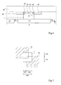
- Figure 1 shows an example of a bipolar transistor of NPN type with isolation by conventional structure box.
- This transistor is formed in an island 1 of an epitaxial layer 2 of type N, itself formed on a monocrystalline silicon wafer 3 of type P.
- a buried layer 4 of type N + is formed at the interface between the layer epitaxial and the substrate and extends in particular under the island 1.
- This island 1 is delimited laterally by a trench 5 filled with silicon oxide which completely surrounds it.
- the trench 5 extends to the upper surface of the buried layer 4. It may be a little more or a little less deep. However, it must not completely pass through the buried layer 4 because otherwise it would no longer be possible to resume collector contact, as will be seen below.
- a buried layer 6 of type P + is formed under the location of the box 5 to perfect the lateral isolation of the island 1.
- the island 1 constitutes the collector of the NPN transistor and the buried layer 4 constitutes its region of resumption of collector contact.
- a P-type base region 7 inside which is formed an N-type emitter region 8.
- a highly doped P-type peripheral region 9 constitutes a region of basic contact resumption.
- the base region 7 results for example from an implantation of boron.
- the emitter region 8 is for example formed from a layer of polycrystalline silicon 11 heavily doped with type N.
- the peripheral region 9 of basic contact recovery is for example formed from a layer of polycrystalline silicon 12 heavily doped with type P.
- a layer of polycrystalline silicon 12 is suitably etched and then a layer of planarized silicon oxide 14 is deposited by any known method.
- the oxide layer 14 is open in the center of the island 1 and filled with polycrystalline silicon 11. It is also open, at the same time as the thick oxide layer 5, to form a trench which joins the buried layer 4.
- This trench is filled with polycrystalline silicon 16 of type N + , for example at the same time as the filling of polycrystalline silicon 11 with emitter. Then, the contacts are resumed in a conventional manner on the upper surfaces of the elements 11, 12 and 16.
- the surface of island 1 corresponds substantially on the surface of the base-collector junction.
- the base-collector capacity (which we wish to reduce to increase the possible operating speed of the transistor) is proportional to this area.
- the present invention aims to improve the characteristics of a bipolar transistor and to reduce the dimensions minimum values of a bipolar transistor, from which it results including an increase in the operating speed of this transistor.
- FIG. 3 represents an embodiment of a transistor according to the present invention at an intermediate stage Manufacturing.
- a recess 22 is formed which extends over only part of the thickness of the silicon oxide layer 5 along at least one edge of the periphery of the island 1.
- a layer of polycrystalline silicon is deposited and it is rewired by any known process to obtain a portion of P-doped polycrystalline silicon 23 filling the recess 22 and whose upper surface is in the plane of the upper surface of island 1.
- the engraving of the polycrystalline silicon is carried out by chemical mechanical polishing which stops on the layer of silicon nitride 20, this layer 20 being eliminated at a later stage.
- the recess 41 is filled with polycrystalline silicon 43 doped type N, in the same way as one filled the recess 21 of P-type doped polycrystalline silicon 23
- a base contact region 32 formed at from polycrystalline silicon 23 and an emitter region 45 formed from polycrystalline silicon 43 is deeper around region 45 due to the lateral or oblique implantation described above.
- a layer of silicon oxide 48 is formed at through which will be drilled openings and formed contacts to regions 23 and 43 and the buried layer 4.
- this process makes it possible to obtain a bipolar transistor of miniaturized NPN type.
- the transmitter which results from lateral diffusion, may have a width less than the minimum possible dimension of an opening in a mask.
- the insulating regions 5, 28, 48 have been indicated as being silicon oxide. We can use any other material or combination of materials having the same functions, i.e. to be insulating and able to be selectively etched compared to silicon.
- the active surface of the transmitter above the collector is then zero.
- the present invention is susceptible of various variants and modifications which will appear to those skilled in the art.
- the various materials used may be replaced by materials having the same functions (doping, characteristics electrical, etching selectivity ).
Landscapes
- Bipolar Transistors (AREA)
Abstract
Description
- la portion de silicium polycristallin 12 présente nécessairement un défaut d'alignement par rapport à l'ílot 1 de la couche épitaxiée ;
- il se pose un problème pour le centrage de l'émetteur par rapport à la base et ceci exige la mise en oeuvre de méthodes relativement sophistiquées pour obtenir un auto-alignement ;
- la couche de silicium polycristallin de base 12 déborde nécessairement d'une certaine quantité, liée aux tolérances de positionnement au-dessus de l'ílot 1 ; il en résulte une contribution non-négligeable à la valeur de la capacité base-collecteur ; et
- le processus décrit implique nécessairement une dimension minimale possible liée aux tolérances de positionnement et aux dimensions minimales de masquage.
- surface de l'ílot 1 : 1,05 x 1,05 µm = 1,1 µm2,
- surface de l'émetteur : 0,55 x 0,55 µm + 0,3 µm2,
- périmètre de l'émetteur : 550 µm x 4 = 2,2 µm.
- hauteur de l'ílot 1 : 0,5 µm,
- largeur de l'ílot 1 : 0,4 µm,
- profondeur des régions 23 et 43 : 0,1 et 0,2 µm,
- largeur des régions 23 et 43 : 0,25 µm,
- épaisseur de l'oxyde 28, 48 : 0,5 µm
- surface de l'ílot 1 : 0,40 x 0,4 µm = 0,16 µm2,
- périmètre d'émetteur : 2 x 0,25 = 0,5 µm.
Claims (5)
- Transistor bipolaire à isolement latéral par caisson (5), dans lequel une première partie de la périphérie interne supérieure du caisson d'isolement est évidée et remplie de silicium polycristallin (23) du type de conductivité de la base du transistor, caractérisé en ce qu'une deuxième partie de la périphérie interne supérieure du caisson isolant est évidée et remplie de silicium polycristallin (43) du type de conductivité de l'émetteur du transistor.
- Transistor bipolaire selon la revendication 1, caractérisé en ce qu'une couche d'un matériau de type SiGe est formée à l'interface entre l'ílot et le silicium polycristallin (43) du type de conductivité de l'émetteur du transistor.
- Procédé de fabrication d'un transistor bipolaire selon la revendication 1, caractérisé en ce qu'il comprend les étapes suivantes :former un ílot (1) d'une couche épitaxiée du premier type de conductivité entourée d'un caisson (5) rempli d'isolant,graver une partie au moins de la périphérie interne supérieure du caisson par un procédé de gravure anisotrope sélectif par rapport à la couche épitaxiée pour former un évidement (22),remplir l'évidement (22) de silicium polycristallin (23) du deuxième type de conductivité,amener la surface supérieure du silicium polycristallin (23) à être au même niveau que la surface supérieure de l'ílot,réaliser une implantation de base (24) du deuxième type de conductivité, etdéposer une deuxième couche de silicium polycristallin (27) du premier type de conductivité sur une partie de l'ílot (1) et de façon décalée par rapport audit évidement.
- Procédé de fabrication d'un transistor bipolaire selon la revendication 1, caractérisé en ce qu'il comprend les étapes suivantes :former un ílot (1) d'une couche épitaxiée du premier type de conductivité entourée d'un caisson (5) rempli d'isolant,graver une première partie de la périphérie interne supérieure du caisson pour former un premier évidement (22),remplir le premier évidement de silicium polycristallin (23) du deuxième type de conductivité,réaliser une implantation de base (24) du deuxième type de conductivité,graver une deuxième partie de la périphérie interne supérieure du caisson d'oxyde pour former un deuxième évidement (41), etremplir le deuxième évidement de silicium polycristallin (43) du premier type de conductivité.
- Procédé selon la revendication 4, caractérisé en ce qu'il comprend l'étape consistant à siliciurer les surfaces apparentes des régions de silicium polycristallin (23, 43).
Applications Claiming Priority (2)
| Application Number | Priority Date | Filing Date | Title |
|---|---|---|---|
| FR9615389A FR2756974B1 (fr) | 1996-12-10 | 1996-12-10 | Transistor bipolaire a isolement par caisson |
| FR9615389 | 1996-12-10 |
Publications (2)
| Publication Number | Publication Date |
|---|---|
| EP0848429A1 true EP0848429A1 (fr) | 1998-06-17 |
| EP0848429B1 EP0848429B1 (fr) | 2003-02-26 |
Family
ID=9498682
Family Applications (1)
| Application Number | Title | Priority Date | Filing Date |
|---|---|---|---|
| EP97410138A Expired - Lifetime EP0848429B1 (fr) | 1996-12-10 | 1997-12-09 | Transistor bipolaire à isolement par caisson |
Country Status (7)
| Country | Link |
|---|---|
| US (3) | US6184102B1 (fr) |
| EP (1) | EP0848429B1 (fr) |
| JP (1) | JP3178400B2 (fr) |
| KR (1) | KR19980063791A (fr) |
| DE (1) | DE69719299D1 (fr) |
| FR (1) | FR2756974B1 (fr) |
| TW (1) | TW406357B (fr) |
Families Citing this family (3)
| Publication number | Priority date | Publication date | Assignee | Title |
|---|---|---|---|---|
| JP2003078518A (ja) * | 2001-09-03 | 2003-03-14 | Fuji Xerox Co Ltd | 暗号化・復号システム、暗号化装置、復号装置およびそれらの方法 |
| FR2829288A1 (fr) * | 2001-09-06 | 2003-03-07 | St Microelectronics Sa | Structure de contact sur une region profonde formee dans un substrat semiconducteur |
| KR100481209B1 (ko) * | 2002-10-01 | 2005-04-08 | 삼성전자주식회사 | 다중 채널을 갖는 모스 트랜지스터 및 그 제조방법 |
Citations (3)
| Publication number | Priority date | Publication date | Assignee | Title |
|---|---|---|---|---|
| US4339767A (en) * | 1980-05-05 | 1982-07-13 | International Business Machines Corporation | High performance PNP and NPN transistor structure |
| EP0378794A1 (fr) * | 1989-01-18 | 1990-07-25 | International Business Machines Corporation | Structure de transistor bipolaire vertical et procédé de fabrication |
| JPH034538A (ja) * | 1989-06-01 | 1991-01-10 | Toshiba Corp | バイポーラ型半導体装置 |
Family Cites Families (11)
| Publication number | Priority date | Publication date | Assignee | Title |
|---|---|---|---|---|
| US4392149A (en) * | 1980-03-03 | 1983-07-05 | International Business Machines Corporation | Bipolar transistor |
| US4338138A (en) * | 1980-03-03 | 1982-07-06 | International Business Machines Corporation | Process for fabricating a bipolar transistor |
| JPS5873156A (ja) * | 1981-10-28 | 1983-05-02 | Hitachi Ltd | 半導体装置 |
| US4703554A (en) * | 1985-04-04 | 1987-11-03 | Texas Instruments Incorporated | Technique for fabricating a sidewall base contact with extrinsic base-on-insulator |
| US4933733A (en) * | 1985-06-03 | 1990-06-12 | Advanced Micro Devices, Inc. | Slot collector transistor |
| US4887145A (en) * | 1985-12-04 | 1989-12-12 | Hitachi, Ltd. | Semiconductor device in which electrodes are formed in a self-aligned manner |
| US4829015A (en) * | 1987-05-21 | 1989-05-09 | Siemens Aktiengesellschaft | Method for manufacturing a fully self-adjusted bipolar transistor |
| US5187554A (en) * | 1987-08-11 | 1993-02-16 | Sony Corporation | Bipolar transistor |
| NL8800157A (nl) * | 1988-01-25 | 1989-08-16 | Philips Nv | Halfgeleiderinrichting en werkwijze ter vervaardiging daarvan. |
| US5128271A (en) | 1989-01-18 | 1992-07-07 | International Business Machines Corporation | High performance vertical bipolar transistor structure via self-aligning processing techniques |
| US4965217A (en) * | 1989-04-13 | 1990-10-23 | International Business Machines Corporation | Method of making a lateral transistor |
-
1996
- 1996-12-10 FR FR9615389A patent/FR2756974B1/fr not_active Expired - Fee Related
-
1997
- 1997-12-04 KR KR1019970065917A patent/KR19980063791A/ko not_active Withdrawn
- 1997-12-08 TW TW086118475A patent/TW406357B/zh not_active IP Right Cessation
- 1997-12-08 US US08/987,095 patent/US6184102B1/en not_active Expired - Lifetime
- 1997-12-09 DE DE69719299T patent/DE69719299D1/de not_active Expired - Lifetime
- 1997-12-09 EP EP97410138A patent/EP0848429B1/fr not_active Expired - Lifetime
- 1997-12-10 JP JP35639597A patent/JP3178400B2/ja not_active Expired - Fee Related
-
1999
- 1999-09-07 US US09/390,891 patent/US6114743A/en not_active Expired - Lifetime
-
2000
- 2000-11-30 US US09/726,939 patent/US6432789B2/en not_active Expired - Lifetime
Patent Citations (3)
| Publication number | Priority date | Publication date | Assignee | Title |
|---|---|---|---|---|
| US4339767A (en) * | 1980-05-05 | 1982-07-13 | International Business Machines Corporation | High performance PNP and NPN transistor structure |
| EP0378794A1 (fr) * | 1989-01-18 | 1990-07-25 | International Business Machines Corporation | Structure de transistor bipolaire vertical et procédé de fabrication |
| JPH034538A (ja) * | 1989-06-01 | 1991-01-10 | Toshiba Corp | バイポーラ型半導体装置 |
Non-Patent Citations (1)
| Title |
|---|
| PATENT ABSTRACTS OF JAPAN vol. 015, no. 114 (E - 1047) 19 March 1991 (1991-03-19) * |
Also Published As
| Publication number | Publication date |
|---|---|
| US6114743A (en) | 2000-09-05 |
| KR19980063791A (ko) | 1998-10-07 |
| US6432789B2 (en) | 2002-08-13 |
| JP3178400B2 (ja) | 2001-06-18 |
| FR2756974A1 (fr) | 1998-06-12 |
| DE69719299D1 (de) | 2003-04-03 |
| EP0848429B1 (fr) | 2003-02-26 |
| TW406357B (en) | 2000-09-21 |
| JPH10178022A (ja) | 1998-06-30 |
| FR2756974B1 (fr) | 1999-06-04 |
| US20010000289A1 (en) | 2001-04-19 |
| US6184102B1 (en) | 2001-02-06 |
Similar Documents
| Publication | Publication Date | Title |
|---|---|---|
| US20050218399A1 (en) | Method of fabrication sige heterojunction bipolar transistor | |
| EP0851488B1 (fr) | Procédé de formation d'un transistor bipolaire à isolement diélectrique | |
| EP1406307A1 (fr) | Circuit intégré à couche enterrée fortement conductrice | |
| FR2778022A1 (fr) | Transistor bibolaire vertical, en particulier a base a heterojonction sige, et procede de fabrication | |
| JPH04215469A (ja) | 相補形バイポーラ・トランジスタの形成方法 | |
| FR2728387A1 (fr) | Procede de fabrication d'un transistor bipolaire | |
| EP3872843A1 (fr) | Procédé de fabrication d'un transistor bipolaire et transistor bipolaire susceptible d'être obtenu par un tel procédé | |
| EP0996146A1 (fr) | Procédé de formation d'un caisson isolé dans une plaquette de silicium | |
| US20030025125A1 (en) | Lateral operation bipolar transistor and a corresponding fabrication process | |
| EP1061568A1 (fr) | Procédé de fabrication autoaligné de transistors bipolaires | |
| EP1058302B1 (fr) | Procédé de fabrication de dispositifs bipolaires à jonction base-émetteur autoalignée | |
| EP0848429B1 (fr) | Transistor bipolaire à isolement par caisson | |
| US5147809A (en) | Method of producing a bipolar transistor with a laterally graded emitter (LGE) employing a refill method of polycrystalline silicon | |
| EP0675544B1 (fr) | Procédé de fabrication d'un transistor à effet de champ à grille isolée de longueur de canal réduite, et transistor correspondant | |
| EP1146561A1 (fr) | Procédé de réalisation d'un transistor bipolaire | |
| CN112151373B (zh) | 用于产生二极管的方法 | |
| EP1006573A1 (fr) | Procédé de fabrication de circuits intégrés BICMOS sur un substrat CMOS classique | |
| FR2762139A1 (fr) | Transistor pnp lateral dans une technologie bicmos | |
| EP0843349A1 (fr) | Procédé de fabrication d'un transistor NPN de surface minimale | |
| US7144789B2 (en) | Method of fabricating complementary bipolar transistors with SiGe base regions | |
| EP1475830A2 (fr) | Procédé de fabrication d'un transistor bipolaire | |
| FR2790867A1 (fr) | Procede de fabrication de transistor bipolaire | |
| EP1139430B1 (fr) | Transistor MOS dans un circuit intégré et procédé de formation de zone active | |
| EP0037764B1 (fr) | Structure de dispositif à semiconducteur à anneau de garde, et à fonctionnement unipolaire | |
| FR3007575A1 (fr) | Procede de fabrication d’un transistor bipolaire vertical compatible avec les procedes de fabrication cmos |
Legal Events
| Date | Code | Title | Description |
|---|---|---|---|
| PUAI | Public reference made under article 153(3) epc to a published international application that has entered the european phase |
Free format text: ORIGINAL CODE: 0009012 |
|
| AK | Designated contracting states |
Kind code of ref document: A1 Designated state(s): AT BE CH DE |
|
| AX | Request for extension of the european patent |
Free format text: AL;LT;LV;MK;RO;SI |
|
| 17P | Request for examination filed |
Effective date: 19981123 |
|
| RAP3 | Party data changed (applicant data changed or rights of an application transferred) |
Owner name: STMICROELECTRONICS S.A. |
|
| AKX | Designation fees paid |
Free format text: DE FR GB IT |
|
| RBV | Designated contracting states (corrected) |
Designated state(s): DE FR GB IT |
|
| 17Q | First examination report despatched |
Effective date: 20011015 |
|
| RAP1 | Party data changed (applicant data changed or rights of an application transferred) |
Owner name: STMICROELECTRONICS S.A. |
|
| GRAG | Despatch of communication of intention to grant |
Free format text: ORIGINAL CODE: EPIDOS AGRA |
|
| GRAG | Despatch of communication of intention to grant |
Free format text: ORIGINAL CODE: EPIDOS AGRA |
|
| GRAH | Despatch of communication of intention to grant a patent |
Free format text: ORIGINAL CODE: EPIDOS IGRA |
|
| GRAH | Despatch of communication of intention to grant a patent |
Free format text: ORIGINAL CODE: EPIDOS IGRA |
|
| GRAA | (expected) grant |
Free format text: ORIGINAL CODE: 0009210 |
|
| AK | Designated contracting states |
Designated state(s): DE FR GB IT |
|
| PG25 | Lapsed in a contracting state [announced via postgrant information from national office to epo] |
Ref country code: IT Free format text: LAPSE BECAUSE OF FAILURE TO SUBMIT A TRANSLATION OF THE DESCRIPTION OR TO PAY THE FEE WITHIN THE PRESCRIBED TIME-LIMIT;WARNING: LAPSES OF ITALIAN PATENTS WITH EFFECTIVE DATE BEFORE 2007 MAY HAVE OCCURRED AT ANY TIME BEFORE 2007. THE CORRECT EFFECTIVE DATE MAY BE DIFFERENT FROM THE ONE RECORDED. Effective date: 20030226 |
|
| REG | Reference to a national code |
Ref country code: GB Ref legal event code: FG4D Free format text: NOT ENGLISH |
|
| REF | Corresponds to: |
Ref document number: 69719299 Country of ref document: DE Date of ref document: 20030403 Kind code of ref document: P |
|
| PG25 | Lapsed in a contracting state [announced via postgrant information from national office to epo] |
Ref country code: DE Free format text: LAPSE BECAUSE OF FAILURE TO SUBMIT A TRANSLATION OF THE DESCRIPTION OR TO PAY THE FEE WITHIN THE PRESCRIBED TIME-LIMIT Effective date: 20030527 |
|
| GBT | Gb: translation of ep patent filed (gb section 77(6)(a)/1977) |
Effective date: 20030508 |
|
| PLBE | No opposition filed within time limit |
Free format text: ORIGINAL CODE: 0009261 |
|
| STAA | Information on the status of an ep patent application or granted ep patent |
Free format text: STATUS: NO OPPOSITION FILED WITHIN TIME LIMIT |
|
| 26N | No opposition filed |
Effective date: 20031127 |
|
| PGFP | Annual fee paid to national office [announced via postgrant information from national office to epo] |
Ref country code: GB Payment date: 20051207 Year of fee payment: 9 |
|
| PGFP | Annual fee paid to national office [announced via postgrant information from national office to epo] |
Ref country code: FR Payment date: 20051208 Year of fee payment: 9 |
|
| GBPC | Gb: european patent ceased through non-payment of renewal fee |
Effective date: 20061209 |
|
| REG | Reference to a national code |
Ref country code: FR Ref legal event code: ST Effective date: 20070831 |
|
| PG25 | Lapsed in a contracting state [announced via postgrant information from national office to epo] |
Ref country code: GB Free format text: LAPSE BECAUSE OF NON-PAYMENT OF DUE FEES Effective date: 20061209 |
|
| PG25 | Lapsed in a contracting state [announced via postgrant information from national office to epo] |
Ref country code: FR Free format text: LAPSE BECAUSE OF NON-PAYMENT OF DUE FEES Effective date: 20070102 |