EP0850723B1 - Dispositif support de plaquette semiconductrice - Google Patents
Dispositif support de plaquette semiconductrice Download PDFInfo
- Publication number
- EP0850723B1 EP0850723B1 EP97310308A EP97310308A EP0850723B1 EP 0850723 B1 EP0850723 B1 EP 0850723B1 EP 97310308 A EP97310308 A EP 97310308A EP 97310308 A EP97310308 A EP 97310308A EP 0850723 B1 EP0850723 B1 EP 0850723B1
- Authority
- EP
- European Patent Office
- Prior art keywords
- wafer
- region
- holding jig
- sintered body
- holding
- Prior art date
- Legal status (The legal status is an assumption and is not a legal conclusion. Google has not performed a legal analysis and makes no representation as to the accuracy of the status listed.)
- Expired - Lifetime
Links
- 239000011148 porous material Substances 0.000 claims description 26
- 238000000034 method Methods 0.000 claims description 21
- 238000005498 polishing Methods 0.000 claims description 8
- 239000004065 semiconductor Substances 0.000 claims description 3
- 235000012431 wafers Nutrition 0.000 description 94
- 239000000428 dust Substances 0.000 description 15
- 238000003754 machining Methods 0.000 description 14
- 230000008569 process Effects 0.000 description 7
- 230000006866 deterioration Effects 0.000 description 5
- 239000000463 material Substances 0.000 description 4
- 230000008901 benefit Effects 0.000 description 3
- 230000000052 comparative effect Effects 0.000 description 3
- 230000000694 effects Effects 0.000 description 3
- 239000011521 glass Substances 0.000 description 3
- 230000002093 peripheral effect Effects 0.000 description 3
- 238000007517 polishing process Methods 0.000 description 3
- 229910001218 Gallium arsenide Inorganic materials 0.000 description 2
- XUIMIQQOPSSXEZ-UHFFFAOYSA-N Silicon Chemical compound [Si] XUIMIQQOPSSXEZ-UHFFFAOYSA-N 0.000 description 2
- 238000004887 air purification Methods 0.000 description 2
- 239000011230 binding agent Substances 0.000 description 2
- 230000007547 defect Effects 0.000 description 2
- 229910052710 silicon Inorganic materials 0.000 description 2
- 239000010703 silicon Substances 0.000 description 2
- 238000005245 sintering Methods 0.000 description 2
- 230000009471 action Effects 0.000 description 1
- 239000000853 adhesive Substances 0.000 description 1
- PNEYBMLMFCGWSK-UHFFFAOYSA-N aluminium oxide Inorganic materials [O-2].[O-2].[O-2].[Al+3].[Al+3] PNEYBMLMFCGWSK-UHFFFAOYSA-N 0.000 description 1
- 239000000919 ceramic Substances 0.000 description 1
- 230000008859 change Effects 0.000 description 1
- 230000003247 decreasing effect Effects 0.000 description 1
- 238000010586 diagram Methods 0.000 description 1
- 230000006872 improvement Effects 0.000 description 1
- 239000000203 mixture Substances 0.000 description 1
- 230000009467 reduction Effects 0.000 description 1
- 239000011347 resin Substances 0.000 description 1
- 229920005989 resin Polymers 0.000 description 1
- 239000004575 stone Substances 0.000 description 1
Images

Classifications
-
- B—PERFORMING OPERATIONS; TRANSPORTING
- B24—GRINDING; POLISHING
- B24B—MACHINES, DEVICES, OR PROCESSES FOR GRINDING OR POLISHING; DRESSING OR CONDITIONING OF ABRADING SURFACES; FEEDING OF GRINDING, POLISHING, OR LAPPING AGENTS
- B24B37/00—Lapping machines or devices; Accessories
- B24B37/27—Work carriers
- B24B37/30—Work carriers for single side lapping of plane surfaces
-
- B—PERFORMING OPERATIONS; TRANSPORTING
- B24—GRINDING; POLISHING
- B24B—MACHINES, DEVICES, OR PROCESSES FOR GRINDING OR POLISHING; DRESSING OR CONDITIONING OF ABRADING SURFACES; FEEDING OF GRINDING, POLISHING, OR LAPPING AGENTS
- B24B7/00—Machines or devices designed for grinding plane surfaces on work, including polishing plane glass surfaces; Accessories therefor
- B24B7/20—Machines or devices designed for grinding plane surfaces on work, including polishing plane glass surfaces; Accessories therefor characterised by a special design with respect to properties of the material of non-metallic articles to be ground
- B24B7/22—Machines or devices designed for grinding plane surfaces on work, including polishing plane glass surfaces; Accessories therefor characterised by a special design with respect to properties of the material of non-metallic articles to be ground for grinding inorganic material, e.g. stone, ceramics, porcelain
- B24B7/228—Machines or devices designed for grinding plane surfaces on work, including polishing plane glass surfaces; Accessories therefor characterised by a special design with respect to properties of the material of non-metallic articles to be ground for grinding inorganic material, e.g. stone, ceramics, porcelain for grinding thin, brittle parts, e.g. semiconductors, wafers
Definitions
- the present invention relates to an improvement on a method for grinding or polishing a wafer using a wafer holding jig for vacuum-holding a semiconductor wafer while the wafer is ground or polished.
- EP-A-0776730 discloses a wafer holding jig for vacuum-holding a wafer, comprising a plate of uniformly porous material in which the pores in a peripheral portion of the plate are sealed by means of an injected resin or the like.
- US-A-4597228 discloses a wafer holding jig for vacuum-holding a wafer, comprising a plate of uniformly porous material and a peripheral member of airtight material encircling the plate. The porous plate has a diameter less than the wafer diameter, whereas the outer diameter of the peripheral member is greater than the wafer diameter.
- a wafer holding jig formed from a fine-grain sintered body ⁇ which has a high strength and which therefore does not deform due to machining pressure ⁇ is used to accurately machine the surface of the wafer into a highly flat surface.
- a holding jig having a plurality of regions having different characters.
- a wafer holding surface for holding a wafer W is formed by a porous fine-grain sintered body 52 and a nonporous fine-grain sintered body 53 surrounding the porous fine-grain sintered body 52.
- the porous fine-grain sintered body 52 is formed by a process in which fine grains are sintered such that a resultant sintered body becomes porous.
- the nonporous fine-grain sintered body 53 is formed by a process in which fine grains are sintered such that a resultant sintered body becomes dense or nonporous.
- Evacuation passages 54 are formed to communicate with the porous fine-grain sintered body 52.
- the wafer W is vacuum-held by means of evacuation through the evacuation passages 54.
- the outer diameter of the porous fine-grain sintered body 52 is generally made smaller than the diameter of the wafer W, so that the vacuum region is formed by the outside nonporous fine-grain sintered body 53 and the wafer W.
- the amount of deformation of the wafer W due to application of machining pressure varies between the portion held by the porous fine-grain sintered body 52 and the portion held by the nonporous fine-grain sintered body 53. Since the amount of load-induced deformation at the portion held by the fine-grain porous sintered body 52 is greater than that at the portion held by the nonporous fine-grain sintered body 53, the stock removal of the machining (amount of material removed by machining) at the center portion becomes smaller. Therefore, the machined wafer has a problem of insufficient flatness (flatness defect) in which the center portion has a larger thickness than does the remaining portion of the wafer.
- An object of the present invention is to provide a method for grinding or polishing a wafer using a wafer holding jig which can prevent deterioration in machining accuracy, which deterioration would otherwise occur due to deformation of a wafer stemming from catch of dust or the like, or unevenness in deformation generated upon application of machining pressure to the wafer.
- the present invention provides a method for grinding or polishing a wafer having a predetermined diameter using a wafer holding jig having a porous holding surface for vacuum-holding a semiconductor wafer while the wafer is ground or polished, wherein the porosity of a centre region of the holding surface is made larger than that of an outside region formed to surround the centre region, said centre region has a first outer diameter selected to be less than said predetermined diameter and the outside region has a second outer diameter selected to be greater than said predetermined diameter.
- the outer diameter of the outside region is made greater than that of the wafer in order to hold the entire wafer by the porous surface, unevenness in the amount of deformation of the wafer upon application of pressure can be suppressed. In addition, since foreign matter such as dust is easily sucked through pores at the porous surface, the wafer becomes less likely to deform.
- the center region can be utilised as a vacuum region.
- an evacuation passage is formed in the wafer holding jig to communicate with the center region without communicating with the outside region.
- the evacuation passage is formed to communicate only with the center region having a large porosity, and evacuation is performed via the evacuation passage, the degree of vacuum in a vacuum region can be increased to thereby improve the holding performance.
- pores in the center region have an average diameter of 60 - 300 ⁇ m, and pores in the outside region have an average diameter of 2 - 50 ⁇ m.
- the reason why the average diameter of the pores in the center region is set to fall within the range of 60 - 300 ⁇ m is that if the average diameter of the pores in the center region falls within the range, the pores of the center region can provide a high performance of sucking dust or the like and reliable evacuation.
- the reason why the average diameter of the pores in the outside region is set to fall within the range of 2 - 50 ⁇ m is that if the average diameter of the pores in the outside region falls within the range, the outside region can reliably define a vacuum region and can prevent occurrence of flatness defect during machining.
- the vacuum region cannot be defined reliably, resulting in a decrease in the holding force; and if the average diameter of the pores in the outside region is set to 2 ⁇ m or less, the flatness failure increases.
- the outer diameter of the center region is 50 - 99% of that of the wafer, and the outer diameter of the outside region is 100 - 200% of that of the wafer.
- the holding surface of the wafer holding jig is divided into a center region and an outside region; the porosity of the center region is made larger than that of the outside region; and the outer diameter of the center region is made less than that of a wafer to be held, while the outer diameter of the outside region is made greater than that of the wafer. Therefore, the entire wafer can be held by the porous surface and unevenness in the amount of deformation upon application of machining pressure can be suppressed. In addition, suction of foreign matter such as dust through pores at the porous surface is facilitated. Since adversary effects caused by the unevenness deformation and catch of foreign matter can be eliminated, the wafer becomes less likely to deform, resulting in an increase in machining accuracy.
- a wafer-holding jig for use in a method of grinding or polishing a wafer according to the present invention is used for holding a brittle wafer, such as a silicon wafer or a GaAs wafer, while the surface of the wafer is ground or polished.
- the wafer-holding jig is designed to improve the flatness of the wafer through accurate holding thereof.
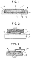
- the holding surface of the wafer holding jig 1 is divided into concentric annular regions A, B, and C, in this sequence from the center of the holding surface toward the outside.
- the regions A, B, and C are formed by a first porous fine-grain sintered body 2, a second porous fine-grain sintered body 3, and a nonporous fine-grain sintered body 4, respectively.
- the porosity of the first porous fine-grain sintered body 2 ⁇ which forms the center region A- is made different from the porosity of the second porous fine-grain sintered body 3 ⁇ which forms the outside region B, which is located immediately outside the center region A.
- the nonporous fine-grain sintered body 4 ⁇ which forms the outermost region C ⁇ is dense or nonporous.
- the pores in the center region A have an average diameter of 60 - 300 ⁇ m in order to provide a relatively large porosity, and the pores in the outside region B have an average diameter of 2 - 50 ⁇ m in order to provide a porosity smaller than that in the center region A.
- the outer diameter of the center region A is smaller than that of the wafer W (50 - 99%), while the outer diameter of the outside region B is greater than that of the wafer W (100 - 200%).
- Evacuation passages 5 serving as vacuum piping are formed in the bottom wall of the nonporous fine-grain sintered body 4 such that the inner ends of the evacuation passages 5 reach the bottom of the first porous fine-grain sintered body 2, which forms the center region A. After a wafer W is placed on the holding jig 1, air in the center region A is evacuated through the evacuation passages 5 in order to vacuum-hold the wafer.
- the degree of vacuum in the center region A can be increased.
- Such a vacuum-type holding jig has an advantage that even when dust or the like enters the space between the wafer W and the holding surface of the holding jig, the dust or the like is sucked through pores at the porous surface by means of evacuation in order to prevent the wafer W from deforming due to dust or the like.
- the holding jig 1 for use in the present invention is designed such that the entire wafer W is held by the porous surface in order to fully utilize the advantage of the vacuum-type holding jig.
- the porosity of the center region A is made larger than that of the outside region B outside the center region A, a vacuum zone can be effectively created in the center region A.
- the wafer-holding jig for use in the method according to the present invention is manufactured by the following method.
- a dense fine-grain sintered body formed of alumina ceramics and having a very low porosity, which is commercially available, is crushed into grains, which are then divided into a large-grain-size group and a small-grain-size group.
- the grains of the large-grain-size group are used as material for the first porous fine-grain sintered body, while the grains of the small-grain-size group are used as material for the second porous fine-grain sintered body.
- Each group of grains is mixed with binder and glass, which serve as adhesive agents, and the mixture is sintered to obtain a sintered body.
- the binder and the glass partially evaporate to form pores.
- the dense (nonporous) fine-grain sintered body is manufactured according to a conventional manner.
- the first porous fine-grain sintered body, the second porous fine-grain sintered body, and the dense or nonporous fine-grain sintered body are bonded together through use of fused glass.
- the holding surface is mechanically machined into a flat surface, so that the wafer holding jig is completed.
- FIG. 2 shows an example in which the holding jig 1 is applied to a polishing process according to the present invention.
- a wafer W is vacuum-held by the holding jig 1 attached to a polishing head 6, and the wafer W is polished by a polishing pad 8 attached to a polishing table 7.
- the dust or the like enters the space between the holding surface of the holding jig 1 and the wafer W during the polishing process, the dust or the like is sucked and therefore does not cause adversary effect such as deformation of the wafer.
- a machining pressure acts on the wafer W, a difference in deformation amount is not produced between the center region A and the outside region B, so that the flatness of the wafer W is not deteriorated.
- FIG. 3 shows an example in which the holding jig 1 is applied to a grinding process according to the present invention.
- a wafer W is vacuum-held by the holding jig 1 attached to a grinding head 10, and the wafer W is ground by a grinding stone 11.
- the wafer W can be machined to have a highly flat surface.
- a holding jig was manufactured such that the center region A had an outer diameter of 130 mm and a pore average diameter of 100 ⁇ m while the outside region B had an outer diameter of 160 mm and a pore average diameter of 10 ⁇ m.
- a wafer W having a diameter of 150 mm was ground through use of the holding jig (Example).
- a conventional holding jig was manufactured such that the center porous fine-grain sintered body 52 had an outer diameter of 140 mm and a pore average diameter of 100 ⁇ m while the outside dense (nonporous) fine-grain sintered body 53 had an outer diameter of 160 mm.
- An identical wafer W was ground through use of the holding jig (Comparative Example).
- Example utilizing the holding Jig in accordance with the present invention was compared with Comparative Example utilizing the conventional holding jig, in terms of machining accuracy.
- FIG. 4 which shows thickness distribution in the ground wafers, when the method of the present invention was used, each wafer was machined to have a highly flat surface without causing a flatness failure. Whereas none of 100 wafers had a flatness failure in Example, 15 of 100 wafers had a flatness failure in Comparative Example.
- the center region A and the outside region B have uniform porosity respectively.
- each of the regions A and B may be divided into subregions in order to change the porosity stepwise.
Landscapes
- Engineering & Computer Science (AREA)
- Mechanical Engineering (AREA)
- Chemical & Material Sciences (AREA)
- Ceramic Engineering (AREA)
- Inorganic Chemistry (AREA)
- Container, Conveyance, Adherence, Positioning, Of Wafer (AREA)
- Mechanical Treatment Of Semiconductor (AREA)
- Jigs For Machine Tools (AREA)
- Finish Polishing, Edge Sharpening, And Grinding By Specific Grinding Devices (AREA)
Claims (5)
- Un procédé pour meuler ou polir une plaquette ayant un diamètre prédéterminé à l'aide d'un instrument destiné à tenir une plaquette ayant une surface de retenue poreuse pour tenir sous vide une plaquette semi-conductrice tandis que la plaquette est meulée ou polie, dans lequel la porosité d'une région centrale de la surface de retenue est rendue plus grande que celle d'une région extérieure formée afin d'entourer la région centrale, ladite région centrale a un premier diamètre externe sélectionné afin d'être inférieur audit diamètre prédéterminé et la région extérieure a un deuxième diamètre externe sélectionné afin d'être plus important que ledit diamètre prédéterminé.
- Un procédé selon la revendication 1, caractérisé en ce qu'un couloir d'évacuation d'air est pratiqué dans l'instrument destiné à tenir une plaquette afin de communiquer avec la région centrale sans communiquer avec la région extérieure.
- Un procédé selon la revendication 1 ou la revendication 2, caractérisé en ce que des pores dans la région centrale ont un diamètre moyen allant de 60 à 300 µm, et des pores dans la région extérieure ont un diamètre moyen allant de 2 à 50 µm.
- Un procédé selon n'importe laquelle des revendications 1 à 3, dans lequel l'instrument destiné à tenir une plaquette comporte en outre une région la plus externe sensiblement non poreuse formée afin d'entourer la région extérieure.
- Un procédé selon n'importe quelle revendication précédente, caractérisé en ce que ledit premier diamètre externe est sélectionné afin d'être compris dans la gamme allant de 50 à 99 % dudit diamètre prédéterminé et ledit deuxième diamètre externe est sélectionné afin d'être compris dans la gamme allant de 100 à 200 % dudit diamètre prédéterminé.
Applications Claiming Priority (3)
| Application Number | Priority Date | Filing Date | Title |
|---|---|---|---|
| JP35798196A JPH10193260A (ja) | 1996-12-27 | 1996-12-27 | ウエーハ保持治具 |
| JP35798196 | 1996-12-27 | ||
| JP357981/96 | 1996-12-27 |
Publications (2)
| Publication Number | Publication Date |
|---|---|
| EP0850723A1 EP0850723A1 (fr) | 1998-07-01 |
| EP0850723B1 true EP0850723B1 (fr) | 2002-11-20 |
Family
ID=18456943
Family Applications (1)
| Application Number | Title | Priority Date | Filing Date |
|---|---|---|---|
| EP97310308A Expired - Lifetime EP0850723B1 (fr) | 1996-12-27 | 1997-12-19 | Dispositif support de plaquette semiconductrice |
Country Status (5)
| Country | Link |
|---|---|
| US (1) | US5938512A (fr) |
| EP (1) | EP0850723B1 (fr) |
| JP (1) | JPH10193260A (fr) |
| DE (1) | DE69717238T2 (fr) |
| TW (1) | TW387110B (fr) |
Families Citing this family (30)
| Publication number | Priority date | Publication date | Assignee | Title |
|---|---|---|---|---|
| JP4236292B2 (ja) * | 1997-03-06 | 2009-03-11 | 日本碍子株式会社 | ウエハー吸着装置およびその製造方法 |
| JPH11138429A (ja) * | 1997-11-11 | 1999-05-25 | Sony Corp | 研磨装置 |
| JP3618220B2 (ja) * | 1998-03-30 | 2005-02-09 | 信越半導体株式会社 | 薄板の研磨方法および薄板保持プレート |
| JPH11300608A (ja) * | 1998-04-20 | 1999-11-02 | Nec Corp | 化学機械研磨装置 |
| ATE309884T1 (de) * | 1998-04-27 | 2005-12-15 | Tokyo Seimitsu Co Ltd | Oberflächenbearbeitungsverfahren und oberflächenbearbeitungsvorrichtung für halbleiterscheiben |
| JP2907209B1 (ja) * | 1998-05-29 | 1999-06-21 | 日本電気株式会社 | ウェハ研磨装置用裏面パッド |
| JP3502550B2 (ja) * | 1998-10-07 | 2004-03-02 | 株式会社東芝 | 研磨装置 |
| US6187681B1 (en) * | 1998-10-14 | 2001-02-13 | Micron Technology, Inc. | Method and apparatus for planarization of a substrate |
| US6344414B1 (en) * | 1999-04-30 | 2002-02-05 | International Business Machines Corporation | Chemical-mechanical polishing system having a bi-material wafer backing film assembly |
| KR100331165B1 (ko) * | 1999-08-05 | 2002-04-01 | 김도열 | 소자 일괄 제조용 지그 및 이를 이용한 소자 일괄 제조방법 |
| WO2001096066A1 (fr) * | 2000-06-15 | 2001-12-20 | Infineon Technologies North America Corp. | Procede de polissage de plaquettes |
| JP3433930B2 (ja) * | 2001-02-16 | 2003-08-04 | 株式会社東京精密 | ウェーハの平面加工装置及びその平面加工方法 |
| JP2003103455A (ja) * | 2001-09-28 | 2003-04-08 | Shin Etsu Handotai Co Ltd | ワーク保持盤並びにワークの研磨装置及び研磨方法 |
| JP3892703B2 (ja) * | 2001-10-19 | 2007-03-14 | 富士通株式会社 | 半導体基板用治具及びこれを用いた半導体装置の製造方法 |
| US7018268B2 (en) * | 2002-04-09 | 2006-03-28 | Strasbaugh | Protection of work piece during surface processing |
| JP2004022899A (ja) * | 2002-06-18 | 2004-01-22 | Shinko Electric Ind Co Ltd | 薄シリコンウエーハの加工方法 |
| JP2005268566A (ja) * | 2004-03-19 | 2005-09-29 | Ebara Corp | 化学機械研磨装置の基板把持機構のヘッド構造 |
| US20060211349A1 (en) * | 2005-03-18 | 2006-09-21 | Seh America, Inc. | Wafer polishing template for polishing semiconductor wafers in a wax free polishing process |
| JP5205737B2 (ja) * | 2006-10-13 | 2013-06-05 | 株式会社Sumco | シリコンウェーハの保持方法および保持治具 |
| US20090036030A1 (en) * | 2007-08-03 | 2009-02-05 | Winbond Electronics Corp. | Polishing head and chemical mechanical polishing process using the same |
| KR101036605B1 (ko) * | 2008-06-30 | 2011-05-24 | 세메스 주식회사 | 기판 지지 유닛 및 이를 이용한 매엽식 기판 연마 장치 |
| JP2011044473A (ja) * | 2009-08-19 | 2011-03-03 | Disco Abrasive Syst Ltd | ウエーハの研削装置 |
| JP2011044472A (ja) * | 2009-08-19 | 2011-03-03 | Disco Abrasive Syst Ltd | ウエーハの研削装置 |
| JP5943742B2 (ja) * | 2012-07-04 | 2016-07-05 | 三菱電機株式会社 | 半導体試験治具およびそれを用いた半導体試験方法 |
| JP2016051749A (ja) * | 2014-08-29 | 2016-04-11 | 京セラ株式会社 | 吸着用部材 |
| JP2016072350A (ja) * | 2014-09-29 | 2016-05-09 | 京セラ株式会社 | 吸着用部材 |
| CN108231648A (zh) * | 2016-12-21 | 2018-06-29 | 山东浪潮华光光电子股份有限公司 | 一种GaAs基LED芯片减薄工艺中的贴片工装及贴片方法 |
| US20180281151A1 (en) * | 2017-03-30 | 2018-10-04 | Applied Materials, Inc. | Adhesive-less carriers for chemical mechanical polishing |
| JP2019111594A (ja) * | 2017-12-21 | 2019-07-11 | 株式会社ディスコ | チャックテーブル |
| CN108838870B (zh) * | 2018-06-05 | 2020-02-14 | 南通瑞森光学股份有限公司 | 一种半导体晶圆研磨设备 |
Family Cites Families (7)
| Publication number | Priority date | Publication date | Assignee | Title |
|---|---|---|---|---|
| US3731435A (en) * | 1971-02-09 | 1973-05-08 | Speedfam Corp | Polishing machine load plate |
| US4521995A (en) * | 1980-05-23 | 1985-06-11 | Disco Co., Ltd. | Wafer attracting and fixing device |
| JPS60103651U (ja) * | 1983-12-19 | 1985-07-15 | シチズン時計株式会社 | 真空吸着台 |
| JPS62297063A (ja) * | 1986-02-21 | 1987-12-24 | Hitachi Ltd | 薄片状部材研磨用真空チヤツク装置 |
| JP2538511B2 (ja) * | 1993-09-21 | 1996-09-25 | 住友シチックス株式会社 | 半導体基板の研磨用保持板 |
| JPH08180026A (ja) * | 1994-12-26 | 1996-07-12 | Fuji Facom Corp | 論理通信路管理方法 |
| JP3072962B2 (ja) * | 1995-11-30 | 2000-08-07 | ロデール・ニッタ株式会社 | 研磨のための被加工物の保持具及びその製法 |
-
1996
- 1996-12-27 JP JP35798196A patent/JPH10193260A/ja active Pending
-
1997
- 1997-12-16 US US08/991,492 patent/US5938512A/en not_active Expired - Fee Related
- 1997-12-16 TW TW086119006A patent/TW387110B/zh not_active IP Right Cessation
- 1997-12-19 EP EP97310308A patent/EP0850723B1/fr not_active Expired - Lifetime
- 1997-12-19 DE DE69717238T patent/DE69717238T2/de not_active Expired - Fee Related
Also Published As
| Publication number | Publication date |
|---|---|
| US5938512A (en) | 1999-08-17 |
| TW387110B (en) | 2000-04-11 |
| JPH10193260A (ja) | 1998-07-28 |
| EP0850723A1 (fr) | 1998-07-01 |
| DE69717238T2 (de) | 2003-08-28 |
| DE69717238D1 (de) | 2003-01-02 |
Similar Documents
| Publication | Publication Date | Title |
|---|---|---|
| US5938512A (en) | Wafer holding jig | |
| US4597228A (en) | Vacuum suction device | |
| US6077149A (en) | Method and apparatus for surface-grinding of workpiece | |
| JP3072962B2 (ja) | 研磨のための被加工物の保持具及びその製法 | |
| JP4666656B2 (ja) | 真空吸着装置、その製造方法および被吸着物の吸着方法 | |
| JP3121886B2 (ja) | 真空吸着装置 | |
| JP4908263B2 (ja) | 真空吸着装置およびその製造方法 | |
| JPH11309638A (ja) | 真空吸着盤 | |
| GB2334205A (en) | Polishing pad for semiconductor wafers | |
| JPH0582631A (ja) | 半導体ウエーハ用真空チヤツク | |
| JPS63251166A (ja) | ウエハチヤツク | |
| US20130270756A1 (en) | Retaining system for retaining and holding a wafer | |
| JP5046859B2 (ja) | 接合体、吸着部材、吸着装置および加工装置 | |
| JP2006093492A (ja) | 真空吸着装置 | |
| JP2001341042A (ja) | 真空チャックおよびその製造方法 | |
| JPH0513051U (ja) | 真空チヤツク | |
| JP2004209633A (ja) | 加工用基板固定装置およびその製造方法 | |
| WO2024117149A1 (fr) | Plateau de maintien à vide et son procédé de production | |
| JP4468059B2 (ja) | 静圧軸受け装置 | |
| JP4948920B2 (ja) | 真空チャック及びこれを用いた真空吸着装置 | |
| JP2000021959A (ja) | 真空吸着盤 | |
| JP2007180102A (ja) | 吸着体の製造方法及び吸着体 | |
| JPH0332537A (ja) | ユニバーサルチャックテーブル | |
| JP2006093491A (ja) | 真空吸着装置 | |
| JPH03213265A (ja) | ラップ盤の定盤 |
Legal Events
| Date | Code | Title | Description |
|---|---|---|---|
| PUAI | Public reference made under article 153(3) epc to a published international application that has entered the european phase |
Free format text: ORIGINAL CODE: 0009012 |
|
| AK | Designated contracting states |
Kind code of ref document: A1 Designated state(s): DE FR GB |
|
| AX | Request for extension of the european patent |
Free format text: AL;LT;LV;MK;RO;SI |
|
| 17P | Request for examination filed |
Effective date: 19980617 |
|
| AKX | Designation fees paid |
Free format text: DE FR GB |
|
| RBV | Designated contracting states (corrected) |
Designated state(s): DE FR GB |
|
| 17Q | First examination report despatched |
Effective date: 20000405 |
|
| GRAG | Despatch of communication of intention to grant |
Free format text: ORIGINAL CODE: EPIDOS AGRA |
|
| GRAG | Despatch of communication of intention to grant |
Free format text: ORIGINAL CODE: EPIDOS AGRA |
|
| GRAH | Despatch of communication of intention to grant a patent |
Free format text: ORIGINAL CODE: EPIDOS IGRA |
|
| GRAH | Despatch of communication of intention to grant a patent |
Free format text: ORIGINAL CODE: EPIDOS IGRA |
|
| GRAA | (expected) grant |
Free format text: ORIGINAL CODE: 0009210 |
|
| AK | Designated contracting states |
Kind code of ref document: B1 Designated state(s): DE FR GB |
|
| REG | Reference to a national code |
Ref country code: GB Ref legal event code: FG4D |
|
| REF | Corresponds to: |
Ref document number: 69717238 Country of ref document: DE Date of ref document: 20030102 |
|
| ET | Fr: translation filed | ||
| PLBE | No opposition filed within time limit |
Free format text: ORIGINAL CODE: 0009261 |
|
| STAA | Information on the status of an ep patent application or granted ep patent |
Free format text: STATUS: NO OPPOSITION FILED WITHIN TIME LIMIT |
|
| 26N | No opposition filed |
Effective date: 20030821 |
|
| PGFP | Annual fee paid to national office [announced via postgrant information from national office to epo] |
Ref country code: FR Payment date: 20041208 Year of fee payment: 8 |
|
| PGFP | Annual fee paid to national office [announced via postgrant information from national office to epo] |
Ref country code: GB Payment date: 20041215 Year of fee payment: 8 |
|
| PGFP | Annual fee paid to national office [announced via postgrant information from national office to epo] |
Ref country code: DE Payment date: 20041216 Year of fee payment: 8 |
|
| PG25 | Lapsed in a contracting state [announced via postgrant information from national office to epo] |
Ref country code: GB Free format text: LAPSE BECAUSE OF NON-PAYMENT OF DUE FEES Effective date: 20051219 |
|
| PG25 | Lapsed in a contracting state [announced via postgrant information from national office to epo] |
Ref country code: DE Free format text: LAPSE BECAUSE OF NON-PAYMENT OF DUE FEES Effective date: 20060701 |
|
| GBPC | Gb: european patent ceased through non-payment of renewal fee |
Effective date: 20051219 |
|
| PG25 | Lapsed in a contracting state [announced via postgrant information from national office to epo] |
Ref country code: FR Free format text: LAPSE BECAUSE OF NON-PAYMENT OF DUE FEES Effective date: 20060831 |
|
| REG | Reference to a national code |
Ref country code: FR Ref legal event code: ST Effective date: 20060831 |