EP0851468A2 - Verfahren zur Herstellung einer integrierten Schaltung mit doppelter Wanne - Google Patents
Verfahren zur Herstellung einer integrierten Schaltung mit doppelter Wanne Download PDFInfo
- Publication number
- EP0851468A2 EP0851468A2 EP97310164A EP97310164A EP0851468A2 EP 0851468 A2 EP0851468 A2 EP 0851468A2 EP 97310164 A EP97310164 A EP 97310164A EP 97310164 A EP97310164 A EP 97310164A EP 0851468 A2 EP0851468 A2 EP 0851468A2
- Authority
- EP
- European Patent Office
- Prior art keywords
- substrate
- region
- illustratively
- tub
- integrated circuit
- Prior art date
- Legal status (The legal status is an assumption and is not a legal conclusion. Google has not performed a legal analysis and makes no representation as to the accuracy of the status listed.)
- Withdrawn
Links
Images


Classifications
-
- H—ELECTRICITY
- H10—SEMICONDUCTOR DEVICES; ELECTRIC SOLID-STATE DEVICES NOT OTHERWISE PROVIDED FOR
- H10P—GENERIC PROCESSES OR APPARATUS FOR THE MANUFACTURE OR TREATMENT OF DEVICES COVERED BY CLASS H10
- H10P30/00—Ion implantation into wafers, substrates or parts of devices
- H10P30/20—Ion implantation into wafers, substrates or parts of devices into semiconductor materials, e.g. for doping
- H10P30/22—Ion implantation into wafers, substrates or parts of devices into semiconductor materials, e.g. for doping using masks
-
- H—ELECTRICITY
- H10—SEMICONDUCTOR DEVICES; ELECTRIC SOLID-STATE DEVICES NOT OTHERWISE PROVIDED FOR
- H10D—INORGANIC ELECTRIC SEMICONDUCTOR DEVICES
- H10D84/00—Integrated devices formed in or on semiconductor substrates that comprise only semiconducting layers, e.g. on Si wafers or on GaAs-on-Si wafers
- H10D84/01—Manufacture or treatment
- H10D84/0123—Integrating together multiple components covered by H10D12/00 or H10D30/00, e.g. integrating multiple IGBTs
- H10D84/0126—Integrating together multiple components covered by H10D12/00 or H10D30/00, e.g. integrating multiple IGBTs the components including insulated gates, e.g. IGFETs
- H10D84/0165—Integrating together multiple components covered by H10D12/00 or H10D30/00, e.g. integrating multiple IGBTs the components including insulated gates, e.g. IGFETs the components including complementary IGFETs, e.g. CMOS devices
- H10D84/0191—Manufacturing their doped wells
-
- H—ELECTRICITY
- H10—SEMICONDUCTOR DEVICES; ELECTRIC SOLID-STATE DEVICES NOT OTHERWISE PROVIDED FOR
- H10D—INORGANIC ELECTRIC SEMICONDUCTOR DEVICES
- H10D84/00—Integrated devices formed in or on semiconductor substrates that comprise only semiconducting layers, e.g. on Si wafers or on GaAs-on-Si wafers
- H10D84/01—Manufacture or treatment
- H10D84/02—Manufacture or treatment characterised by using material-based technologies
- H10D84/03—Manufacture or treatment characterised by using material-based technologies using Group IV technology, e.g. silicon technology or silicon-carbide [SiC] technology
- H10D84/038—Manufacture or treatment characterised by using material-based technologies using Group IV technology, e.g. silicon technology or silicon-carbide [SiC] technology using silicon technology, e.g. SiGe
Definitions
- This invention relates to-methods of making integrated circuits with twin tubs.
- CMOS integrated circuits utilize a substrate with twin tubs.
- One tub is typically doped with an n-type dopant, while the other tub is doped with a p-type dopant.
- An example of a twin tub patent is found in U. S. Patent No. 4,435,896, issued to Parillo et al.
- An artifact of some twin tub manufacturing processes is a height difference between the upper silicon surface of n tub and the p tub.
- the silicon surface of the p tub is not co-planar with the silicon surface of the n tub.
- This lack of co-planarity may contribute to difficulties in achieving proper stepper focus as integrated circuitry dimensions shrink. (Subsequent attempts to remove or reduce the lack of co-planarity may require extra masks and incur extra costs.)
- the present invention includes
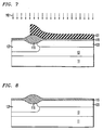
- FIGS. 1-8 are cross-sectional views of useful in understanding illustrative embodiments of the present invention.
- reference numeral 11 illustratively denotes a p-type substrate.
- substrate 11 may be n-type or intrinsic also.
- the term substrate refers to a material upon which other materials may be formed.
- Other suitable substrates are gallium arsenide and its alloys, gallium nitride, etc. Indium phosphide and its alloys may also be a suitable substrate.
- Reference numeral 13 denotes, illustratively, an optional layer of p-type epitaxial material, illustratively having a thickness between 2 and 15 microns.
- Reference numeral 15 denotes a pad oxide layer illustratively having a thickness between 350 - 450 ⁇ .
- Pad oxide 15 may illustratively be formed by exposure of substrate 11 to an oxidizing ambient at a temperature of approximately 1000°. Other methods are possible and known to those skill in the art.
- Reference numeral 17 denotes a photoresist which has been patterned to cover and protect a portion of the substrate.
- an optional removal of a portion of exposed pad oxide 15 may be performed to provide a clean upper oxide surface.
- 0.5 microns of pad oxide 15 may be removed in a plasma etch
- an ion implantation 191 of either one or more different n-type species is performed.
- two separate implants of the same n-type species may be performed.
- a first shallow implant of phosphorus may be performed followed by a second deeper implant of arsenic.
- each of the implants may be performed at energies between 0 and 300 KeV and dosage ranges between 1E11 to 5E16/cm 2 . Appropriate species, energies and dosages may be chosen by those of skill in the art depending upon the types of circuits desired.
- n-type implant species within epitaxial layer 13 are denoted by reference numeral 23.
- FIG. 2 shows that the portion of the pad oxide 15 over region 23 has been reduced by the optional plasma etch mentioned above.
- the region denoted by reference numeral 23 will, upon subsequent annealing, become the n-tub.
- a protective material 21 is deposited principally over the already-implanted n region 23.
- a portion of protective layer 21 may also be deposited upon upper surface 19 of photoresist 17.
- Suitable protective materials are: spin on glass, polyimide, titanium nitride formed by spin-on processes, planarized low temperature glass and any other material with an etch rate differential with respect to photoresist 17.
- the thickness of protective material 21 is chosen so that material 21 is capable of protecting n tub 23 from subsequently implanted p-type species as will be explained below.
- protective material 21 may be blanket deposited and then the entire wafer planarized with chemical-mechanical polishing (CMP), or a deposit-etch-deposit etc. process may be performed.
- CMP chemical-mechanical polishing
- any portion of protective material 21 which is formed on upper surface 19 of photoresist 17 is removed by a light clean-up etch or CMP, etc.
- photoresist 17 has been removed.
- one or two p-type dopant species are implanted into epitaxial layer 13.
- two separate boron implants one implant being deep, the other shallow, are performed thereby creating a P region 27.
- P region 27 is slightly deeper than n region 23, although this need not be always necessarily true.
- protective material 21 is removed. It will be noted, by examination of FIG. 4, that when oxide layer 15 is removed, that the upper surface 31 of n tub 23 is co-planar with upper surface 29 of p tub 27.
- P region 27 and a region 23 may be annealed to create corresponding p tubs and n tubs.
- Field oxides may be defined by LOCOS or poly-buffered LOCOS or other processes known in the art.
- gates may be defined and dielectric layers and metallization formed.
- Figs. 5-8 illustrate another embodiment of the invention in which the field oxide has been formed prior to tub definition.
- reference numeral 11 denotes a substrate
- reference numeral 13 denotes an optional epitaxial overlayer
- Reference numeral 115 denotes a pad oxide layer
- reference numeral 116 denotes a field oxide.
- Field oxide 116 may, illustratively, be formed by a LOCOS process or a poly-buffered LOCOS process.
- Reference numeral 17 denotes a photoresist which is patterned to cover and protect a portion of the substrate. Again, an optional removal of a portion of exposed pad oxide 115 may be performed. Then an ion implantation 191 of one or more different implant species is performed. Illustrative implant energies and dosages have already been described. Turning to Fig. 2, the implant species define region 123. Next, a protective material 121 is deposited. Suitable candidate materials for protective material 121 have already been discussed.
- Fig. 3 photoresist 17, together with any overlying material has been removed.
- One or two dopant species 192 is then implanted to form region 127.
- regions 123 and 127 may be annealed to form complementary tubs. Further processing according to standard methods may proceed at this point.
- Gates may define and dielectric layers and metallization formed.
Landscapes
- Metal-Oxide And Bipolar Metal-Oxide Semiconductor Integrated Circuits (AREA)
- Element Separation (AREA)
- Formation Of Insulating Films (AREA)
Applications Claiming Priority (2)
| Application Number | Priority Date | Filing Date | Title |
|---|---|---|---|
| US775490 | 1996-12-31 | ||
| US08/775,490 US6017787A (en) | 1996-12-31 | 1996-12-31 | Integrated circuit with twin tub |
Publications (2)
| Publication Number | Publication Date |
|---|---|
| EP0851468A2 true EP0851468A2 (de) | 1998-07-01 |
| EP0851468A3 EP0851468A3 (de) | 1998-08-05 |
Family
ID=25104593
Family Applications (1)
| Application Number | Title | Priority Date | Filing Date |
|---|---|---|---|
| EP97310164A Withdrawn EP0851468A3 (de) | 1996-12-31 | 1997-12-16 | Verfahren zur Herstellung einer integrierten Schaltung mit doppelter Wanne |
Country Status (5)
| Country | Link |
|---|---|
| US (1) | US6017787A (de) |
| EP (1) | EP0851468A3 (de) |
| JP (1) | JP3253908B2 (de) |
| KR (1) | KR100554648B1 (de) |
| TW (1) | TW410438B (de) |
Families Citing this family (10)
| Publication number | Priority date | Publication date | Assignee | Title |
|---|---|---|---|---|
| US6566181B2 (en) * | 1999-02-26 | 2003-05-20 | Agere Systems Inc. | Process for the fabrication of dual gate structures for CMOS devices |
| US6391700B1 (en) * | 2000-10-17 | 2002-05-21 | United Microelectronics Corp. | Method for forming twin-well regions of semiconductor devices |
| US6518107B2 (en) * | 2001-02-16 | 2003-02-11 | Advanced Micro Devices, Inc. | Non-arsenic N-type dopant implantation for improved source/drain interfaces with nickel silicides |
| US6900091B2 (en) * | 2002-08-14 | 2005-05-31 | Advanced Analogic Technologies, Inc. | Isolated complementary MOS devices in epi-less substrate |
| US7825488B2 (en) | 2006-05-31 | 2010-11-02 | Advanced Analogic Technologies, Inc. | Isolation structures for integrated circuits and modular methods of forming the same |
| US6855985B2 (en) * | 2002-09-29 | 2005-02-15 | Advanced Analogic Technologies, Inc. | Modular bipolar-CMOS-DMOS analog integrated circuit & power transistor technology |
| KR100697289B1 (ko) * | 2005-08-10 | 2007-03-20 | 삼성전자주식회사 | 반도체 장치의 형성 방법 |
| US7407851B2 (en) * | 2006-03-22 | 2008-08-05 | Miller Gayle W | DMOS device with sealed channel processing |
| JP2007273588A (ja) * | 2006-03-30 | 2007-10-18 | Fujitsu Ltd | 半導体装置の製造方法 |
| JP6216142B2 (ja) * | 2012-05-28 | 2017-10-18 | キヤノン株式会社 | 半導体装置の製造方法 |
Citations (1)
| Publication number | Priority date | Publication date | Assignee | Title |
|---|---|---|---|---|
| EP0164737A2 (de) * | 1984-06-15 | 1985-12-18 | Harris Corporation | Verfahren zum Herstellen selbstjustierter Bereiche in einem Substrat |
Family Cites Families (18)
| Publication number | Priority date | Publication date | Assignee | Title |
|---|---|---|---|---|
| JPS5613722A (en) * | 1979-07-13 | 1981-02-10 | Matsushita Electric Ind Co Ltd | Manufacture of semiconductor device |
| US4435896A (en) * | 1981-12-07 | 1984-03-13 | Bell Telephone Laboratories, Incorporated | Method for fabricating complementary field effect transistor devices |
| US4558508A (en) * | 1984-10-15 | 1985-12-17 | International Business Machines Corporation | Process of making dual well CMOS semiconductor structure with aligned field-dopings using single masking step |
| JPS6197859A (ja) * | 1984-10-18 | 1986-05-16 | Matsushita Electronics Corp | 相補型mos集積回路の製造方法 |
| US4584027A (en) * | 1984-11-07 | 1986-04-22 | Ncr Corporation | Twin well single mask CMOS process |
| US5141882A (en) * | 1989-04-05 | 1992-08-25 | Mitsubishi Denki Kabushiki Kaisha | Semiconductor field effect device having channel stop and channel region formed in a well and manufacturing method therefor |
| JPH081930B2 (ja) * | 1989-09-11 | 1996-01-10 | 株式会社東芝 | 半導体装置の製造方法 |
| JPH0483335A (ja) * | 1990-07-25 | 1992-03-17 | Fujitsu Ltd | 半導体装置の製造方法 |
| US5217570A (en) * | 1991-01-31 | 1993-06-08 | Sony Corporation | Dry etching method |
| US5300797A (en) * | 1992-03-31 | 1994-04-05 | Sgs-Thomson Microelectronics, Inc. | Coplanar twin-well integrated circuit structure |
| JP2978345B2 (ja) * | 1992-11-26 | 1999-11-15 | 三菱電機株式会社 | 半導体装置の製造方法 |
| JPH0745713A (ja) * | 1993-07-29 | 1995-02-14 | Kawasaki Steel Corp | 半導体装置の製造方法 |
| JP3391410B2 (ja) * | 1993-09-17 | 2003-03-31 | 富士通株式会社 | レジストマスクの除去方法 |
| US5413944A (en) * | 1994-05-06 | 1995-05-09 | United Microelectronics Corporation | Twin tub CMOS process |
| US5422312A (en) * | 1994-06-06 | 1995-06-06 | United Microelectronics Corp. | Method for forming metal via |
| US5573963A (en) * | 1995-05-03 | 1996-11-12 | Vanguard International Semiconductor Corporation | Method of forming self-aligned twin tub CMOS devices |
| US5573962A (en) * | 1995-12-15 | 1996-11-12 | Vanguard International Semiconductor Corporation | Low cycle time CMOS process |
| US5670395A (en) * | 1996-04-29 | 1997-09-23 | Chartered Semiconductor Manufacturing Pte. Ltd. | Process for self-aligned twin wells without N-well and P-well height difference |
-
1996
- 1996-12-31 US US08/775,490 patent/US6017787A/en not_active Expired - Lifetime
-
1997
- 1997-12-16 EP EP97310164A patent/EP0851468A3/de not_active Withdrawn
- 1997-12-26 JP JP36017697A patent/JP3253908B2/ja not_active Expired - Lifetime
- 1997-12-31 KR KR1019970081732A patent/KR100554648B1/ko not_active Expired - Fee Related
-
1998
- 1998-01-14 TW TW086120081A patent/TW410438B/zh not_active IP Right Cessation
Patent Citations (1)
| Publication number | Priority date | Publication date | Assignee | Title |
|---|---|---|---|---|
| EP0164737A2 (de) * | 1984-06-15 | 1985-12-18 | Harris Corporation | Verfahren zum Herstellen selbstjustierter Bereiche in einem Substrat |
Also Published As
| Publication number | Publication date |
|---|---|
| US6017787A (en) | 2000-01-25 |
| EP0851468A3 (de) | 1998-08-05 |
| JP3253908B2 (ja) | 2002-02-04 |
| JPH10209297A (ja) | 1998-08-07 |
| KR19980064838A (ko) | 1998-10-07 |
| TW410438B (en) | 2000-11-01 |
| KR100554648B1 (ko) | 2006-04-21 |
Similar Documents
| Publication | Publication Date | Title |
|---|---|---|
| US5766991A (en) | CMOS process utilizing disposable silicon nitride spacers for making lightly doped drain | |
| US4717683A (en) | CMOS process | |
| US5250445A (en) | Discretionary gettering of semiconductor circuits | |
| JPH07142567A (ja) | Soi膜厚制御法 | |
| JPS6037775A (ja) | 集積回路構成体の製造方法 | |
| JP2521611B2 (ja) | ツインウェルを有するcmosの製造方法 | |
| US6017787A (en) | Integrated circuit with twin tub | |
| JP2003197557A (ja) | 選択可能なゲート厚を有する集積回路およびその製造方法 | |
| US6048778A (en) | Gettering regions and methods of forming gettering regions within a semiconductor wafer | |
| JP3701326B2 (ja) | 集積回路の素子分離方法 | |
| EP0564191A2 (de) | Struktur und Verfahren zur Herstellung von integrierten Schaltungen | |
| US5895251A (en) | Method for forming a triple-well in a semiconductor device | |
| JPH06112483A (ja) | Soi基板を用いた半導体装置の製造方法 | |
| US5106768A (en) | Method for the manufacture of CMOS FET by P+ maskless technique | |
| US5780347A (en) | Method of forming polysilicon local interconnects | |
| US6703187B2 (en) | Method of forming a self-aligned twin well structure with a single mask | |
| US5518938A (en) | Process for fabricating a CMOS transistor having high-voltage metal-gate | |
| US5994190A (en) | Semiconductor device with impurity layer as channel stopper immediately under silicon oxide film | |
| US6110788A (en) | Surface channel MOS transistors, methods for making the same, and semiconductor devices containing the same | |
| WO2004095522A2 (en) | Deep n wells in triple well structures and method for fabricating same | |
| US5486482A (en) | Process for fabricating metal-gate CMOS transistor | |
| EP0809286B1 (de) | Verfahren zur Herstellung von Halbleiterbauteilen mit verschiedenartigen vergrabenen Dotierungsgebieten | |
| US20040097051A1 (en) | Methods for improving well to well isolation | |
| US5811864A (en) | Planarized integrated circuit product and method for making it | |
| KR100188000B1 (ko) | 반도체 소자의 웰 형성 방법 |
Legal Events
| Date | Code | Title | Description |
|---|---|---|---|
| PUAI | Public reference made under article 153(3) epc to a published international application that has entered the european phase |
Free format text: ORIGINAL CODE: 0009012 |
|
| PUAL | Search report despatched |
Free format text: ORIGINAL CODE: 0009013 |
|
| AK | Designated contracting states |
Kind code of ref document: A2 Designated state(s): DE ES FR GB IT NL |
|
| AX | Request for extension of the european patent |
Free format text: AL;LT;LV;MK;RO;SI |
|
| AK | Designated contracting states |
Kind code of ref document: A3 Designated state(s): AT BE CH DE DK ES FI FR GB GR IE IT LI LU MC NL PT SE |
|
| AX | Request for extension of the european patent |
Free format text: AL;LT;LV;MK;RO;SI |
|
| 17P | Request for examination filed |
Effective date: 19990121 |
|
| AKX | Designation fees paid |
Free format text: DE ES FR GB IT NL |
|
| RBV | Designated contracting states (corrected) |
Designated state(s): DE ES FR GB IT NL |
|
| 17Q | First examination report despatched |
Effective date: 20040924 |
|
| RAP3 | Party data changed (applicant data changed or rights of an application transferred) |
Owner name: LUCENT TECHNOLOGIES INC. |
|
| RAP1 | Party data changed (applicant data changed or rights of an application transferred) |
Owner name: ALCATEL-LUCENT USA INC. |
|
| RAP1 | Party data changed (applicant data changed or rights of an application transferred) |
Owner name: LUCENT TECHNOLOGIES INC. |
|
| STAA | Information on the status of an ep patent application or granted ep patent |
Free format text: STATUS: EXAMINATION IS IN PROGRESS |
|
| R17C | First examination report despatched (corrected) |
Effective date: 20040924 |
|
| R17C | First examination report despatched (corrected) |
Effective date: 20040924 |
|
| STAA | Information on the status of an ep patent application or granted ep patent |
Free format text: STATUS: THE APPLICATION IS DEEMED TO BE WITHDRAWN |
|
| 18D | Application deemed to be withdrawn |
Effective date: 20190216 |