EP0851569B1 - Leistungswandler mit verbesserter Hauptschaltersteuerung und mehreren Spannungspegeln - Google Patents
Leistungswandler mit verbesserter Hauptschaltersteuerung und mehreren Spannungspegeln Download PDFInfo
- Publication number
- EP0851569B1 EP0851569B1 EP97403133A EP97403133A EP0851569B1 EP 0851569 B1 EP0851569 B1 EP 0851569B1 EP 97403133 A EP97403133 A EP 97403133A EP 97403133 A EP97403133 A EP 97403133A EP 0851569 B1 EP0851569 B1 EP 0851569B1
- Authority
- EP
- European Patent Office
- Prior art keywords
- current
- auxiliary
- rail
- voltage
- converter
- Prior art date
- Legal status (The legal status is an assumption and is not a legal conclusion. Google has not performed a legal analysis and makes no representation as to the accuracy of the status listed.)
- Expired - Lifetime
Links
- 239000003990 capacitor Substances 0.000 claims abstract description 27
- 230000010355 oscillation Effects 0.000 claims abstract description 17
- 108010077333 CAP1-6D Proteins 0.000 claims description 4
- 101000897856 Homo sapiens Adenylyl cyclase-associated protein 2 Proteins 0.000 claims description 4
- 101000836079 Homo sapiens Serpin B8 Proteins 0.000 claims description 4
- 101000798702 Homo sapiens Transmembrane protease serine 4 Proteins 0.000 claims description 4
- 102100029500 Prostasin Human genes 0.000 claims description 4
- 102100032471 Transmembrane protease serine 4 Human genes 0.000 claims description 4
- 238000001514 detection method Methods 0.000 claims description 4
- 108010031970 prostasin Proteins 0.000 claims description 4
- 238000000034 method Methods 0.000 claims description 3
- 230000004044 response Effects 0.000 claims description 3
- 230000008878 coupling Effects 0.000 claims description 2
- 238000010168 coupling process Methods 0.000 claims description 2
- 238000005859 coupling reaction Methods 0.000 claims description 2
- 230000008569 process Effects 0.000 claims description 2
- 230000000977 initiatory effect Effects 0.000 abstract 1
- 230000003534 oscillatory effect Effects 0.000 abstract 1
- 230000008901 benefit Effects 0.000 description 4
- 238000011156 evaluation Methods 0.000 description 4
- 230000001960 triggered effect Effects 0.000 description 3
- 238000010586 diagram Methods 0.000 description 2
- 101000869912 Cerastes vipera Disintegrin CV-11-alpha Proteins 0.000 description 1
- 230000005355 Hall effect Effects 0.000 description 1
- 230000009471 action Effects 0.000 description 1
- 230000004913 activation Effects 0.000 description 1
- 230000008033 biological extinction Effects 0.000 description 1
- 230000000903 blocking effect Effects 0.000 description 1
- 230000036772 blood pressure Effects 0.000 description 1
- 238000004364 calculation method Methods 0.000 description 1
- 210000004027 cell Anatomy 0.000 description 1
- 230000008859 change Effects 0.000 description 1
- 239000004020 conductor Substances 0.000 description 1
- 238000010276 construction Methods 0.000 description 1
- 230000003247 decreasing effect Effects 0.000 description 1
- 230000001627 detrimental effect Effects 0.000 description 1
- 239000006185 dispersion Substances 0.000 description 1
- 230000000694 effects Effects 0.000 description 1
- 238000005516 engineering process Methods 0.000 description 1
- 230000001939 inductive effect Effects 0.000 description 1
- 238000004519 manufacturing process Methods 0.000 description 1
- 230000021715 photosynthesis, light harvesting Effects 0.000 description 1
Images


Classifications
-
- H—ELECTRICITY
- H02—GENERATION; CONVERSION OR DISTRIBUTION OF ELECTRIC POWER
- H02M—APPARATUS FOR CONVERSION BETWEEN AC AND AC, BETWEEN AC AND DC, OR BETWEEN DC AND DC, AND FOR USE WITH MAINS OR SIMILAR POWER SUPPLY SYSTEMS; CONVERSION OF DC OR AC INPUT POWER INTO SURGE OUTPUT POWER; CONTROL OR REGULATION THEREOF
- H02M7/00—Conversion of AC power input into DC power output; Conversion of DC power input into AC power output
- H02M7/42—Conversion of DC power input into AC power output without possibility of reversal
- H02M7/44—Conversion of DC power input into AC power output without possibility of reversal by static converters
- H02M7/48—Conversion of DC power input into AC power output without possibility of reversal by static converters using discharge tubes with control electrode or semiconductor devices with control electrode
- H02M7/505—Conversion of DC power input into AC power output without possibility of reversal by static converters using discharge tubes with control electrode or semiconductor devices with control electrode using devices of a thyratron or thyristor type requiring extinguishing means
- H02M7/515—Conversion of DC power input into AC power output without possibility of reversal by static converters using discharge tubes with control electrode or semiconductor devices with control electrode using devices of a thyratron or thyristor type requiring extinguishing means using semiconductor devices only
- H02M7/519—Conversion of DC power input into AC power output without possibility of reversal by static converters using discharge tubes with control electrode or semiconductor devices with control electrode using devices of a thyratron or thyristor type requiring extinguishing means using semiconductor devices only in a push-pull configuration
-
- H—ELECTRICITY
- H02—GENERATION; CONVERSION OR DISTRIBUTION OF ELECTRIC POWER
- H02M—APPARATUS FOR CONVERSION BETWEEN AC AND AC, BETWEEN AC AND DC, OR BETWEEN DC AND DC, AND FOR USE WITH MAINS OR SIMILAR POWER SUPPLY SYSTEMS; CONVERSION OF DC OR AC INPUT POWER INTO SURGE OUTPUT POWER; CONTROL OR REGULATION THEREOF
- H02M7/00—Conversion of AC power input into DC power output; Conversion of DC power input into AC power output
- H02M7/42—Conversion of DC power input into AC power output without possibility of reversal
- H02M7/44—Conversion of DC power input into AC power output without possibility of reversal by static converters
- H02M7/48—Conversion of DC power input into AC power output without possibility of reversal by static converters using discharge tubes with control electrode or semiconductor devices with control electrode
- H02M7/505—Conversion of DC power input into AC power output without possibility of reversal by static converters using discharge tubes with control electrode or semiconductor devices with control electrode using devices of a thyratron or thyristor type requiring extinguishing means
- H02M7/515—Conversion of DC power input into AC power output without possibility of reversal by static converters using discharge tubes with control electrode or semiconductor devices with control electrode using devices of a thyratron or thyristor type requiring extinguishing means using semiconductor devices only
- H02M7/523—Conversion of DC power input into AC power output without possibility of reversal by static converters using discharge tubes with control electrode or semiconductor devices with control electrode using devices of a thyratron or thyristor type requiring extinguishing means using semiconductor devices only with LC-resonance circuit in the main circuit
- H02M7/5233—Conversion of DC power input into AC power output without possibility of reversal by static converters using discharge tubes with control electrode or semiconductor devices with control electrode using devices of a thyratron or thyristor type requiring extinguishing means using semiconductor devices only with LC-resonance circuit in the main circuit the commutation elements being in a push-pull arrangement
- H02M7/5236—Conversion of DC power input into AC power output without possibility of reversal by static converters using discharge tubes with control electrode or semiconductor devices with control electrode using devices of a thyratron or thyristor type requiring extinguishing means using semiconductor devices only with LC-resonance circuit in the main circuit the commutation elements being in a push-pull arrangement in a series push-pull arrangement
Definitions
- the present invention relates to so-called soft switching power, especially power converters described in the article "High Power Transistor Inverters - Potential for Single Device Operation at 1000 A and 800 V ", by G. A. Fisher, published in the minutes of the "16th Universities Power Engineering Conference “, Sheffield, Great Britain, in the article “Resonant Snubbers with Auxiliary Switches", by W. McMurray, published in IEEE Transactions on Industry Applications, Vol. 29, No. 2, March / April 1993 and in the patent document WO 92/05625.
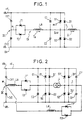
- the components S1, D1, C1, T1, CV1 are respectively paired with components S2, D2, C2, T2, CV2, i.e. show respectively in all occasions with the same electrical characteristics.
- a circuit control unit not shown measures voltages and currents in various points of the converter comprising this arm and, according to an appropriate program, controls the triggering of main switches S1 and S2 and switches auxiliaries T1 and T2, by action on electrodes command which are only sketched in the figure, in ec1 for example, as will now be described.
- the switching of the circuit begins with a first step in which the auxiliary switch T1 is triggered by the control circuit. It becomes conductive and the auxiliary inductance LA finds itself supplied between + V / 2 (at the threshold of T1 near) and 0 V (at the threshold of D2 near); the current I A which crosses it increases linearly. This current is subtracted from the current I L in the diode D2.
- the switch S1 is then triggered, with no voltage at its terminals and takes over the current I L.
- the inductance LA now connected between the point M, at the potential + V / 2, and the output S, maintained at the potential + V through the switch T1, sees the current I A which crosses it decreasing linearly.
- the auxiliary switch T1 is blocked.
- a thyristor type switch is used, which has the property of blocking when the current flowing through it is canceled, or any equivalent combination of components, a transistor or an IGBT in series with a diode, for example.
- the changeover in the other direction, to return to the initial situation is accomplished in a similar way, by having recourse to the auxiliary circuit CA whose auxiliary switch T2 is triggered, as above the auxiliary switch T1.
- the switch S1 is then controlled to also block.
- the voltage of the output S then goes from + V to 0 volts in an oscillation at the end of which the auxiliary switch T2 is blocked, the diode D2 then becoming conductive under the effect of the current I L.
- the voltage tilting of the output S of a converter arm takes place without losses if the voltage on this output S actually goes from 0 to + V volts, i.e. if the voltage across the circuit auxiliary AC reverses, i.e. again if the voltage at point M is indeed equal to + V / 2.
- the capacities capacitors CV1 and CV2 of the DC voltage divider must be large enough, the symmetry of components involved in the conduction phases of the auxiliary circuit must be almost perfect, as should the resistive losses in this auxiliary circuit. experience shows that these conditions are difficult to fulfill and this is a problem.
- any imperfection in the above is reflected in the fact that at the end of the alternation of the oscillation considered, the voltage at point S is not + V / 2, but a lower voltage, so that the potential difference between the switch terminals principal S1 is not null and that this one is returned conductor while residual voltage remains at its terminals, which will cause energy dissipation in the main switch, detrimental in that the heat resulting must be evacuated and that the yield of the converter will be lessened.
- the present invention is based on the observation that the application of this classic solution leads to accepting maximum losses for safety reasons, then that in fact this is generally excessive.
- the components used have dispersions inside of defined tolerances.
- the calculation of the above threshold is done so considering the corresponding worst case to such tolerances.
- Set the threshold on a case-by-case basis request specific measures in manufacturing and test, as well as means to define an adjustable threshold. This is not economically viable.
- the converter does not always work at maximum charge ; this is particularly the case in the AC operation, but also in the most DC applications.
- the threshold is set so as to meet conditions of most unfavorable walks which are only rarely met and the satisfaction of security needs further translated into excessive loss of efficiency.
- the invention therefore proposes to the additional problem posed a more satisfactory solution, not comprising economically unacceptable requirements, providing significant advantages in terms of converter efficiency power.
- the power converter defined above comprises means for detecting, in a switching process intended for conduction of a main switch targeted and comprising for this purpose a conduction of the auxiliary circuit, a current oscillation between said auxiliary inductance and said tilting capacitors and then the interruption of this oscillation current, and to cause the setting conduction of said targeted main switch, in response to said interruption.
- the invention is thus based on the fact that the voltage across the capacitors is minimal at the end of a half oscillation period, when the oscillation current cancels. Now is the optimal time to conduction the main switch targeted, the losses being minimum.
- said detection comprises a quasi-permanent evaluation of the current in said circuit auxiliary and in a load circuit, the difference between these two currents representing said oscillation current.
- said detection comprises a quasi-permanent evaluation of the current in said tilting capacitors and in particular of the extinction of this current.
- the example of implementation of the invention shown in Figure 3 is intended to control the operation of the converter arm of Figure 1, or that of one of Figure 2 converter arm.
- the Figure 3 device includes current sensors allowing an almost permanent evaluation of the current in the driver with whom they are placed, including one first sensor CAP1, associated with the auxiliary circuit CA, and more particularly evaluating the current in the inductance auxiliary LA, a second sensor CAP2, doing the same in regarding the current in the load, and / or a third CC1 sensor and a fourth CC2 sensor, evaluating respectively the current in the capacitors of tilting C1 and C2.
- sensors are connected to a DCM walking control device which also receives run command instructions via an ICM input and other information on the operation of the converter by an IFC input; it provides in particular the signals of command CT1 and CT2 which control the operation of auxiliary switches T1 and T2, as well as signals CS1 and CS2 which control the operation of the switches main S1 and S2.
- the DCM running control device informed about the state of the converter by the signals coming from the sensors represented and, by other signals coming from sensors not represented reaching him on his IFC input, contains a walking program and, in response to control signals from an unrepresented external source, reaching him on his ICM input, controls the switching of the converter conduction state in another.
- the DCM device first makes the auxiliary switch T1 conductive , the current is established and increases in the auxiliary circuit AC, and the current in the diode D2 thus ends up canceling out. At this moment the oscillation begins, the current of which will discharge the tilting capacitor C1 and charge the tilting capacitor C2.
- the DCM running control device detects the start of this oscillation by the evolution of the voltage at point S (communicated by an ad hoc sensor), the decrease in current in the capacitor C2, detected by the sensor CC2, or the increase in the current in the capacitor C1, detected by the sensor CC1, in the case where these sensors CC1 and CC2 are provided, or even by other means that the person skilled in the art will easily imagine.
- the DCM device enters a phase in which it must detect the interruption of the oscillation current, at the end of the half-period oscillation.
- this event is detected by the fact that the current is canceled in the tilting capacitor C1, detected by the CC1 sensor, or the current in the capacitor tilting C2, detected by the CC2 sensor.
- This second solution is equivalent to the previous one.
- the skilled person can find other ways to detect this event.
- the invention consists basically in what we use this event, duly detected, to order the conduction of the main switch in question.
- FIG. 4 shows a three-level converter of the type described in the article "Three level auxiliary resonant commutated pole inveter for high power applications "by J. G. Cho et al already mentioned.
- the invention applies in each of the control circuits CC1 (main switch S1 and freewheeling diode D1), CC2 (main switch S2 and freewheeling diode D2), CC3 (main switch S3 and freewheeling diode D3), CC4 (main switch S4 and freewheeling diode D4), relationship with the current charging the capacitors C1, C2, C3, under the control of the auxiliary circuits CA1, CA2, coupled to sockets VA1, VA2, VA3, of a voltage divider capacitive CV11, CV12, CV13, CV14, by means not represented but in every respect similar to those who have just been described with reference to FIGS. 1 to 3, as will readily be understood by those skilled in the art.
- the main switch control thus improved allows to make a main switch conductive then that the residual voltage at its terminals is always minimum and therefore limit the losses of the power converter, which still allows, to technology equals to increase performance.
Landscapes
- Engineering & Computer Science (AREA)
- Power Engineering (AREA)
- Dc-Dc Converters (AREA)
- Inverter Devices (AREA)
- Ac-Ac Conversion (AREA)
Claims (3)
- Leistungswandler, enthaltend mindestens einen Arm, der zwischen einer positiven Schiene (VR+) und einer negativen Schiene (VR-)wobei der Wandler unter anderem Mittel (CAP1, CAP2; CC1, CC2; DCM) enthält, um bei einem Umschaltvorgang, der dazu bestimmt ist, einen bestimmten Hauptschalter (S1; S2) in einen leitenden Zustand zu versetzen und der es zu diesem Zweck einschließt, den Hilfsstromkreis (CA) in einen leitenden Zustand zu versetzen, eine Schwingung des Stroms zwischen dem induktiven Hilfswiderstand (LA) und den Umschaltkondensatoren (C1, C2) und anschließend die Unterbrechung dieses Schwingstroms zu erfassen und um ansprechend auf die Unterbrechung den bestimmten Hauptschalter (S1; S2) in einen leitenden Zustand zu versetzen,zwei Hauptschalter (S 1 und S2), die es ermöglichen, einen Ausgang (S), der eine Ladung (L) führt, jeweils entweder mit der positiven Schiene (VR+) oder mit der negativen Schiene (VR-) zu verbinden;zwei Freilaufdioden (D1 und D2), welche die Aufrechterhaltung des Stroms in der Ladung (L) ermöglichen, indem sie den Ausgang (S) jeweils mit der positiven Schiene (VR+) oder mit der negativen Schiene (VR-) koppeln,zwei Umschaltkondensatoren (C1 und C2) zwischen dem Ausgang (S) und der positiven Schiene (VR+) bzw. der negativen Schiene (VR-),einen Hilfsstromkreis (CA) enthält, der insbesondere einen induktiven Hilfswiderstand (LA) in Reihenschaltung mit zwei gegenüberliegenden, in einer Richtung leitenden Hilfsschaltern (T1 und T2) enthält, die zwischen den Ausgang (S) und einen Mittelpunkt (M) eines Spannungsteilerkondensators (DC) geschaltet sind, der selbst zwei Spannungsteilerkondensatoren (CV1 und CV2) enthält, die zwischen der positiven Schiene (VR+) und der negativen Schiene (VR-) in Reihe geschaltet sind, und an diesem Mittelpunkt nominal eine Mittelwertspannung im Vergleich zu derjenigen der positiven Schiene (VR+) und der negativen Schiene (VR-) liefert,
dadurch gekennzeichnet, dass die Erfassung eine quasi-permanente Bewertung des Stroms im Hilfsstromkreis (CA) und im Lastkreis (L) umfasst, wobei die Differenz zwischen den beiden Strömen den Schwingstrom darstellt. - Wandler nach Anspruch 1, dadurch gekennzeichnet, dass die Erfassung eine quasi-permanente Bewertung des Stroms in den Umschaltkondensatoren (C1, C2) und insbesondere des Abklingens dieses Stroms umfasst.
- Anwendung der Einrichtungen, die den Gegenstand eines der vorhergehenden Ansprüche bilden, in den verschiedenen Stufen eines Leistungswandlers mit drei oder mehr Spannungspegeln.
Applications Claiming Priority (2)
| Application Number | Priority Date | Filing Date | Title |
|---|---|---|---|
| FR9616191A FR2758019B1 (fr) | 1996-12-30 | 1996-12-30 | Convertisseur de puissance a commande amelioree des commutateurs principaux |
| FR9616191 | 1996-12-30 |
Publications (2)
| Publication Number | Publication Date |
|---|---|
| EP0851569A1 EP0851569A1 (de) | 1998-07-01 |
| EP0851569B1 true EP0851569B1 (de) | 2003-06-11 |
Family
ID=9499279
Family Applications (1)
| Application Number | Title | Priority Date | Filing Date |
|---|---|---|---|
| EP97403133A Expired - Lifetime EP0851569B1 (de) | 1996-12-30 | 1997-12-23 | Leistungswandler mit verbesserter Hauptschaltersteuerung und mehreren Spannungspegeln |
Country Status (6)
| Country | Link |
|---|---|
| US (1) | US6046920A (de) |
| EP (1) | EP0851569B1 (de) |
| JP (1) | JP4019130B2 (de) |
| AT (1) | ATE242934T1 (de) |
| DE (1) | DE69722756T2 (de) |
| FR (1) | FR2758019B1 (de) |
Families Citing this family (29)
| Publication number | Priority date | Publication date | Assignee | Title |
|---|---|---|---|---|
| US7272021B2 (en) * | 1997-01-24 | 2007-09-18 | Synqor, Inc. | Power converter with isolated and regulated stages |
| US7269034B2 (en) * | 1997-01-24 | 2007-09-11 | Synqor, Inc. | High efficiency power converter |
| JP2002514378A (ja) * | 1997-01-24 | 2002-05-14 | シンクォール・インコーポレーテッド | 高効率電力変換装置 |
| US6720107B1 (en) * | 1998-06-09 | 2004-04-13 | Farnow Technologies Pty. Ltd. | Redox gel battery |
| AU2001242322A1 (en) * | 2000-04-03 | 2001-10-15 | Aalborg Universitet | A resonant converter |
| DK174165B1 (da) * | 2000-10-13 | 2002-08-05 | American Power Conversion Denm | Resonanskonverter |
| US20040125618A1 (en) * | 2002-12-26 | 2004-07-01 | Michael De Rooij | Multiple energy-source power converter system |
| US6798675B1 (en) * | 2003-06-13 | 2004-09-28 | The United States Of America As Represented By The Secretary Of The Air Force | Charging a capacitive energy store using energy trapping and adaptive clocking |
| US8672732B2 (en) * | 2006-01-19 | 2014-03-18 | Schneider Electric It Corporation | Cooling system and method |
| KR100759897B1 (ko) | 2006-08-02 | 2007-09-18 | 삼성전자주식회사 | 전류 검출 회로 및 방법 |
| US7787261B2 (en) * | 2006-11-01 | 2010-08-31 | Synqor, Inc. | Intermediate bus architecture with a quasi-regulated bus converter |
| RU2321942C1 (ru) * | 2007-02-02 | 2008-04-10 | Государственное образовательное учреждение высшего профессионального образования "Ульяновский государственный университет" | Полумостовой тиристорный инвертор |
| DK2147585T3 (en) | 2007-05-15 | 2017-01-16 | Schneider Electric It Corp | PROCEDURE AND SYSTEM FOR HANDLING EQUIPMENT AND COOLING |
| US8228046B2 (en) * | 2009-06-16 | 2012-07-24 | American Power Conversion Corporation | Apparatus and method for operating an uninterruptible power supply |
| US8503201B2 (en) | 2009-12-03 | 2013-08-06 | Schneider Electric It Corporation | Transient clamping circuitry for voltage converter |
| US8878389B2 (en) | 2011-01-11 | 2014-11-04 | Schneider Electric It Corporation | Method and apparatus for providing uninterruptible power |
| US9024474B2 (en) | 2011-08-03 | 2015-05-05 | Schneider Electric It Corporation | UPS mechanical transfer relay arc mitigation |
| JP5842465B2 (ja) * | 2011-08-29 | 2016-01-13 | 株式会社リコー | 電源装置 |
| US8884464B2 (en) | 2011-08-29 | 2014-11-11 | Schneider Electric It Corporation | Twin boost converter with integrated charger for UPS system |
| US9952103B2 (en) | 2011-12-22 | 2018-04-24 | Schneider Electric It Corporation | Analysis of effect of transient events on temperature in a data center |
| EP2796025A4 (de) | 2011-12-22 | 2016-06-29 | Schneider Electric It Corp | System und verfahren zur vorhersage der temperaturwerte in einem elektronischen system |
| US9099934B2 (en) * | 2012-01-10 | 2015-08-04 | Yaskawa America, Inc. | Three phase active rectifier system |
| US9431921B2 (en) * | 2012-05-01 | 2016-08-30 | Analogic Corporation | Controlling capacitive snubber as function of current in inverter |
| US10459464B2 (en) | 2012-09-03 | 2019-10-29 | Schneider Electric It Corporation | Method and apparatus for controlling distribution of power |
| EP2800265A1 (de) * | 2013-05-03 | 2014-11-05 | ALSTOM Technology Ltd | Wandler |
| US10199950B1 (en) | 2013-07-02 | 2019-02-05 | Vlt, Inc. | Power distribution architecture with series-connected bus converter |
| JP6266171B2 (ja) | 2014-09-12 | 2018-01-24 | フィリップス ライティング ホールディング ビー ヴィ | 電源回路 |
| EP3340448B1 (de) * | 2016-12-23 | 2023-06-07 | Delta Electronics (Thailand) Public Co., Ltd. | Elektrischer leistungswandler mit dämpferschaltung |
| WO2023168514A1 (en) * | 2022-03-03 | 2023-09-14 | Hillcrest Energy Technologies Ltd. | Auxiliary resonant commutated pole converter with self voltage balancing capability |
Family Cites Families (8)
| Publication number | Priority date | Publication date | Assignee | Title |
|---|---|---|---|---|
| US3207974A (en) * | 1961-02-23 | 1965-09-21 | Gen Electric | Inverter circuits |
| US3935528A (en) * | 1974-03-15 | 1976-01-27 | Brown, Boveri & Cie, A.G. | Self-commutating inverter means |
| US4482946A (en) * | 1982-09-27 | 1984-11-13 | Canadian Patents And Development Limited | Hybrid inverter |
| US4471421A (en) * | 1982-09-30 | 1984-09-11 | General Electric Company | Means for controlling a forced commutated hybrid a-c to d-c electric rectifying bridge to avoid reverse recovery overvoltage in the diode leg |
| DE3927888A1 (de) * | 1989-08-24 | 1991-02-28 | Philips Patentverwaltung | Wechselrichteranordnung |
| DE4009020A1 (de) * | 1990-03-21 | 1991-09-26 | Philips Patentverwaltung | Serienresonanz-wechselrichter, insbesondere fuer einen roentgengenerator |
| EP0469172B1 (de) * | 1990-08-02 | 1995-01-25 | Asea Brown Boveri Ag | Viertelbrückenschaltung für grosse Ströme |
| US5047913A (en) * | 1990-09-17 | 1991-09-10 | General Electric Company | Method for controlling a power converter using an auxiliary resonant commutation circuit |
-
1996
- 1996-12-30 FR FR9616191A patent/FR2758019B1/fr not_active Expired - Fee Related
-
1997
- 1997-12-23 DE DE69722756T patent/DE69722756T2/de not_active Expired - Lifetime
- 1997-12-23 EP EP97403133A patent/EP0851569B1/de not_active Expired - Lifetime
- 1997-12-23 AT AT97403133T patent/ATE242934T1/de not_active IP Right Cessation
- 1997-12-26 JP JP36076197A patent/JP4019130B2/ja not_active Expired - Fee Related
- 1997-12-29 US US08/998,812 patent/US6046920A/en not_active Expired - Lifetime
Also Published As
| Publication number | Publication date |
|---|---|
| FR2758019B1 (fr) | 1999-01-22 |
| DE69722756D1 (de) | 2003-07-17 |
| JPH10257784A (ja) | 1998-09-25 |
| EP0851569A1 (de) | 1998-07-01 |
| JP4019130B2 (ja) | 2007-12-12 |
| ATE242934T1 (de) | 2003-06-15 |
| US6046920A (en) | 2000-04-04 |
| DE69722756T2 (de) | 2004-04-29 |
| FR2758019A1 (fr) | 1998-07-03 |
Similar Documents
| Publication | Publication Date | Title |
|---|---|---|
| EP0851569B1 (de) | Leistungswandler mit verbesserter Hauptschaltersteuerung und mehreren Spannungspegeln | |
| EP0654887B1 (de) | Unterbrechungsfreie Stromversorgung mit gemeinsamem Nullleiter und Doppelaufwärtskonverter | |
| EP0898357A1 (de) | Gleichstromwandlervorrichtung | |
| FR3034924A1 (fr) | Convertisseur alternatif-continu a limitation du courant d'appel | |
| FR2943188A1 (fr) | Dispositif de charge rapide pour un vehicule electrique. | |
| FR2753850A1 (fr) | Convertisseur de puissance a commutation douce comprenant des moyens de correction de la tension mediane d'un diviseur de tension capacitif | |
| EP3109988A1 (de) | Leistungswandler mit korrekturschaltkreis des leistungsfaktors | |
| EP2320553B1 (de) | Stromumwandlungsvorrichtung und unterbrechungsfreie Stromversorgung, die eine solche Vorrichtung umfasst | |
| JPH0357117Y2 (de) | ||
| EP0147280B1 (de) | Speiseverfahren und -vorrichtung für eine Last, insbesondere einen Gleichstrommotor für Doppelspannungseisenbahnlokomotiven | |
| EP0107539A1 (de) | Steuerschaltung für einen Synchronmotor mit zwei Ankerwicklungen | |
| WO2024068487A1 (fr) | Circuit d'alimentation électrique d'une unité de stockage d'énergie électrique de véhicule | |
| EP4080747A1 (de) | Elektronische vorrichtung und verfahren zur steuerung eines elektrischen energiewandlers mit einem piezoelektrischen element und entsprechendes elektronisches system zur umwandlung von elektrischer energie | |
| EP3965299A1 (de) | Vorrichtung zur steuerung eines thyristors | |
| EP0087115B1 (de) | Versorgungs- und Steuerungseinheit einer mit verstellbarer Geschwindigkeit laufenden Synchronmaschine | |
| US4244017A (en) | Third harmonic auxiliary commutated inverter having selectable commutation capacitance as a function of load current | |
| EP3966922B1 (de) | Mehrstufiger spannungswandler mit optimierter zusätzlicher energiespeicherung | |
| EP0600809A1 (de) | Wechselstrom-dynamische Ausgleichvorrichtung | |
| FR2849551A1 (fr) | Alimentation basse tension isolee | |
| FR2563393A1 (fr) | Ensemble de commutation a semi-conducteur monodirectionnel en courant et bidirectionnel en tension a blocage commande et a amorcage spontane et graduateur capacitif | |
| JPS62250876A (ja) | 電圧形インバ−タ装置 | |
| FR3157031A1 (fr) | Dispositif électronique et procédé de pilotage, avec suppression d’au moins une phase énergisante, d’un convertisseur d’énergie électrique comportant5 un résonateur piézoélectrique, système de conversion d’énergie électrique associé | |
| WO2025082858A1 (fr) | Circuit d'alimentation électrique d'une unité de stockage d'énergie électrique de véhicule | |
| EP1324478A2 (de) | Hochspannungswandler mit schneller Antwortzeit | |
| FR3130095A1 (fr) | Convertisseur d’énergie électrique avec au moins un couple d’ensembles piézoélectriques et au moins un interrupteur complémentaire de connexion directe entre eux, système de conversion et procédé de pilotage associés |
Legal Events
| Date | Code | Title | Description |
|---|---|---|---|
| PUAI | Public reference made under article 153(3) epc to a published international application that has entered the european phase |
Free format text: ORIGINAL CODE: 0009012 |
|
| AK | Designated contracting states |
Kind code of ref document: A1 Designated state(s): AT BE CH DE ES FR GB IT LI SE |
|
| RAP3 | Party data changed (applicant data changed or rights of an application transferred) |
Owner name: ALCATEL |
|
| 17P | Request for examination filed |
Effective date: 19990104 |
|
| AKX | Designation fees paid |
Free format text: AT BE CH DE ES FR GB IT LI SE |
|
| RBV | Designated contracting states (corrected) |
Designated state(s): AT BE CH DE ES FR GB IT LI SE |
|
| RAP3 | Party data changed (applicant data changed or rights of an application transferred) |
Owner name: ALCATEL |
|
| 17Q | First examination report despatched |
Effective date: 20001123 |
|
| GRAH | Despatch of communication of intention to grant a patent |
Free format text: ORIGINAL CODE: EPIDOS IGRA |
|
| RTI1 | Title (correction) |
Free format text: POWER CONVERTER WITH IMPROVED CONTROL OF MAIN SWITCHES AND WITH SEVERAL VOLTAGE LEVELS |
|
| GRAH | Despatch of communication of intention to grant a patent |
Free format text: ORIGINAL CODE: EPIDOS IGRA |
|
| GRAA | (expected) grant |
Free format text: ORIGINAL CODE: 0009210 |
|
| AK | Designated contracting states |
Designated state(s): AT BE CH DE ES FR GB IT LI SE |
|
| PG25 | Lapsed in a contracting state [announced via postgrant information from national office to epo] |
Ref country code: AT Free format text: LAPSE BECAUSE OF FAILURE TO SUBMIT A TRANSLATION OF THE DESCRIPTION OR TO PAY THE FEE WITHIN THE PRESCRIBED TIME-LIMIT Effective date: 20030611 |
|
| REG | Reference to a national code |
Ref country code: GB Ref legal event code: FG4D Free format text: NOT ENGLISH |
|
| REG | Reference to a national code |
Ref country code: CH Ref legal event code: EP |
|
| REF | Corresponds to: |
Ref document number: 69722756 Country of ref document: DE Date of ref document: 20030717 Kind code of ref document: P |
|
| GBT | Gb: translation of ep patent filed (gb section 77(6)(a)/1977) |
Effective date: 20030806 |
|
| PG25 | Lapsed in a contracting state [announced via postgrant information from national office to epo] |
Ref country code: SE Free format text: LAPSE BECAUSE OF FAILURE TO SUBMIT A TRANSLATION OF THE DESCRIPTION OR TO PAY THE FEE WITHIN THE PRESCRIBED TIME-LIMIT Effective date: 20030911 |
|
| PG25 | Lapsed in a contracting state [announced via postgrant information from national office to epo] |
Ref country code: ES Free format text: LAPSE BECAUSE OF FAILURE TO SUBMIT A TRANSLATION OF THE DESCRIPTION OR TO PAY THE FEE WITHIN THE PRESCRIBED TIME-LIMIT Effective date: 20030922 |
|
| PG25 | Lapsed in a contracting state [announced via postgrant information from national office to epo] |
Ref country code: LI Free format text: LAPSE BECAUSE OF NON-PAYMENT OF DUE FEES Effective date: 20031231 Ref country code: CH Free format text: LAPSE BECAUSE OF NON-PAYMENT OF DUE FEES Effective date: 20031231 Ref country code: BE Free format text: LAPSE BECAUSE OF NON-PAYMENT OF DUE FEES Effective date: 20031231 |
|
| PLBE | No opposition filed within time limit |
Free format text: ORIGINAL CODE: 0009261 |
|
| STAA | Information on the status of an ep patent application or granted ep patent |
Free format text: STATUS: NO OPPOSITION FILED WITHIN TIME LIMIT |
|
| 26N | No opposition filed |
Effective date: 20040312 |
|
| BERE | Be: lapsed |
Owner name: *ALCATEL Effective date: 20031231 |
|
| REG | Reference to a national code |
Ref country code: CH Ref legal event code: PL |
|
| REG | Reference to a national code |
Ref country code: GB Ref legal event code: 732E Free format text: REGISTERED BETWEEN 20100311 AND 20100317 |
|
| REG | Reference to a national code |
Ref country code: FR Ref legal event code: TP |
|
| PGFP | Annual fee paid to national office [announced via postgrant information from national office to epo] |
Ref country code: DE Payment date: 20121207 Year of fee payment: 16 |
|
| PGFP | Annual fee paid to national office [announced via postgrant information from national office to epo] |
Ref country code: GB Payment date: 20121219 Year of fee payment: 16 Ref country code: IT Payment date: 20121217 Year of fee payment: 16 |
|
| PGFP | Annual fee paid to national office [announced via postgrant information from national office to epo] |
Ref country code: FR Payment date: 20130115 Year of fee payment: 16 |
|
| REG | Reference to a national code |
Ref country code: DE Ref legal event code: R119 Ref document number: 69722756 Country of ref document: DE |
|
| GBPC | Gb: european patent ceased through non-payment of renewal fee |
Effective date: 20131223 |
|
| REG | Reference to a national code |
Ref country code: DE Ref legal event code: R119 Ref document number: 69722756 Country of ref document: DE Effective date: 20140701 |
|
| REG | Reference to a national code |
Ref country code: FR Ref legal event code: ST Effective date: 20140829 |
|
| PG25 | Lapsed in a contracting state [announced via postgrant information from national office to epo] |
Ref country code: DE Free format text: LAPSE BECAUSE OF NON-PAYMENT OF DUE FEES Effective date: 20140701 |
|
| PG25 | Lapsed in a contracting state [announced via postgrant information from national office to epo] |
Ref country code: FR Free format text: LAPSE BECAUSE OF NON-PAYMENT OF DUE FEES Effective date: 20131231 Ref country code: GB Free format text: LAPSE BECAUSE OF NON-PAYMENT OF DUE FEES Effective date: 20131223 |
|
| PG25 | Lapsed in a contracting state [announced via postgrant information from national office to epo] |
Ref country code: IT Free format text: LAPSE BECAUSE OF NON-PAYMENT OF DUE FEES Effective date: 20131231 |
|
| PG25 | Lapsed in a contracting state [announced via postgrant information from national office to epo] |
Ref country code: IT Free format text: LAPSE BECAUSE OF NON-PAYMENT OF DUE FEES Effective date: 20131223 |