EP0851642A2 - Mehrträgerempfänger mit Ausgleich von Frequenzverschiebungen und von frequenzabhängigen Verzerrungen - Google Patents
Mehrträgerempfänger mit Ausgleich von Frequenzverschiebungen und von frequenzabhängigen Verzerrungen Download PDFInfo
- Publication number
- EP0851642A2 EP0851642A2 EP97310598A EP97310598A EP0851642A2 EP 0851642 A2 EP0851642 A2 EP 0851642A2 EP 97310598 A EP97310598 A EP 97310598A EP 97310598 A EP97310598 A EP 97310598A EP 0851642 A2 EP0851642 A2 EP 0851642A2
- Authority
- EP
- European Patent Office
- Prior art keywords
- frequency
- modulated signal
- signal
- variation
- compensating
- Prior art date
- Legal status (The legal status is an assumption and is not a legal conclusion. Google has not performed a legal analysis and makes no representation as to the accuracy of the status listed.)
- Granted
Links
Images

Classifications
-
- H—ELECTRICITY
- H04—ELECTRIC COMMUNICATION TECHNIQUE
- H04L—TRANSMISSION OF DIGITAL INFORMATION, e.g. TELEGRAPHIC COMMUNICATION
- H04L25/00—Baseband systems
- H04L25/02—Details ; arrangements for supplying electrical power along data transmission lines
- H04L25/03—Shaping networks in transmitter or receiver, e.g. adaptive shaping networks
- H04L25/03006—Arrangements for removing intersymbol interference
- H04L25/03159—Arrangements for removing intersymbol interference operating in the frequency domain
-
- H—ELECTRICITY
- H04—ELECTRIC COMMUNICATION TECHNIQUE
- H04L—TRANSMISSION OF DIGITAL INFORMATION, e.g. TELEGRAPHIC COMMUNICATION
- H04L27/00—Modulated-carrier systems
- H04L27/26—Systems using multi-frequency codes
- H04L27/2601—Multicarrier modulation systems
- H04L27/2647—Arrangements specific to the receiver only
- H04L27/2649—Demodulators
- H04L27/2653—Demodulators with direct demodulation of individual subcarriers
-
- H—ELECTRICITY
- H04—ELECTRIC COMMUNICATION TECHNIQUE
- H04L—TRANSMISSION OF DIGITAL INFORMATION, e.g. TELEGRAPHIC COMMUNICATION
- H04L27/00—Modulated-carrier systems
- H04L27/26—Systems using multi-frequency codes
- H04L27/2601—Multicarrier modulation systems
- H04L27/2647—Arrangements specific to the receiver only
- H04L27/2655—Synchronisation arrangements
- H04L27/2657—Carrier synchronisation
-
- H—ELECTRICITY
- H04—ELECTRIC COMMUNICATION TECHNIQUE
- H04L—TRANSMISSION OF DIGITAL INFORMATION, e.g. TELEGRAPHIC COMMUNICATION
- H04L27/00—Modulated-carrier systems
- H04L27/26—Systems using multi-frequency codes
- H04L27/2601—Multicarrier modulation systems
- H04L27/2647—Arrangements specific to the receiver only
- H04L27/2655—Synchronisation arrangements
- H04L27/2662—Symbol synchronisation
-
- H—ELECTRICITY
- H04—ELECTRIC COMMUNICATION TECHNIQUE
- H04L—TRANSMISSION OF DIGITAL INFORMATION, e.g. TELEGRAPHIC COMMUNICATION
- H04L27/00—Modulated-carrier systems
- H04L27/26—Systems using multi-frequency codes
- H04L27/2601—Multicarrier modulation systems
- H04L27/2647—Arrangements specific to the receiver only
- H04L27/2655—Synchronisation arrangements
- H04L27/2668—Details of algorithms
- H04L27/2673—Details of algorithms characterised by synchronisation parameters
- H04L27/2676—Blind, i.e. without using known symbols
-
- H—ELECTRICITY
- H04—ELECTRIC COMMUNICATION TECHNIQUE
- H04L—TRANSMISSION OF DIGITAL INFORMATION, e.g. TELEGRAPHIC COMMUNICATION
- H04L25/00—Baseband systems
- H04L25/02—Details ; arrangements for supplying electrical power along data transmission lines
- H04L25/03—Shaping networks in transmitter or receiver, e.g. adaptive shaping networks
- H04L25/03006—Arrangements for removing intersymbol interference
- H04L2025/0335—Arrangements for removing intersymbol interference characterised by the type of transmission
- H04L2025/03375—Passband transmission
- H04L2025/03414—Multicarrier
-
- H—ELECTRICITY
- H04—ELECTRIC COMMUNICATION TECHNIQUE
- H04L—TRANSMISSION OF DIGITAL INFORMATION, e.g. TELEGRAPHIC COMMUNICATION
- H04L25/00—Baseband systems
- H04L25/02—Details ; arrangements for supplying electrical power along data transmission lines
- H04L25/03—Shaping networks in transmitter or receiver, e.g. adaptive shaping networks
- H04L25/03006—Arrangements for removing intersymbol interference
- H04L2025/03433—Arrangements for removing intersymbol interference characterised by equaliser structure
- H04L2025/03439—Fixed structures
- H04L2025/03522—Frequency domain
Definitions
- the present invention relates to a demodulating method for multi-frequency quadrature modulation in digital wireless communications.
- the technique of multi-frequency quadrature modulation is a method for transmission of digital data by frequency multiplexed transmission using a plurality of carrier wave frequencies which are distributed at intervals of the reciprocal of a symbol period.
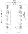
- Fig.1 shows a configuration for a conventional method of multi-frequency quadrature modulation. The operation of the conventional method of multi-frequency quadrature modulation will be described hereinbelow with reference to Fig.1.
- a binary digital signal being input from an input terminal 1 in a transmitter 10 is processed in a digital modulator 11 where the input signal is phase modulated (modulated by PSK: phase shift keying) or quadrature amplitude modulated (modulated by QAM: quadrature amplitude modulation) so as to be converted into an equivalent low-band symbol of the signal.
- PSK phase shift keying
- QAM quadrature amplitude modulation
- the modulated symbol is input to a serial-to-parallel converter (S/P) 12 where it is converted into N number of symbol streams which each have a transmission rate 1/N as much as that of the input symbol stream.
- S/P serial-to-parallel converter
- These streams are processed in an inverse discrete Fourier transformer (IDFT) 13 where the symbol streams are imprinted onto subcarriers having corresponding frequencies and composited to be output.
- IDFT inverse discrete Fourier transformer
- the output signal is a summation signal of a plurality of modulated signals which are distributed at intervals of the reciprocal of the symbol period.
- the output signal from IDFT 13 is converted into serial data by a parallel-to-serial converter 14. Guard intervals are inserted into the converted data by a guard interval inserting section 15.
- the signal with guard intervals inserted therein is then quadrature modulated by a quadrature modulator 16, and the resultant signal is output from a modulated signal output terminal 2 so as to be transmitted.
- a receiver 20 operates in the reverse order to that performed in transmitter 10 so as to interpret the transmitted data stream.
- the received signal is input from an input terminal 3 and is quadrature demodulated by a quadrature demodulator 21.
- the quadrature demodulated signal is stripped of the guard interval components through a guard interval remover 22.
- a symbol synchronous signal is generated by a symbol synchronous signal generating circuit 27.
- the signal which has been stripped of guard intervals is converted into parallel data by a serial-to-parallel converting circuit 23.
- the converted data is input to a discrete Fourier transformer (DFT) 24.
- DFT circuit 24 the received signal is separated into equivalent low-band signals each corresponding to a subchannel so as to be output as parallel data consisting of N symbols.
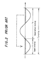
- Fig.2 shows an overall waveform of a modulated signal in the multi-frequency quadrature modulating method.
- the guard interval has the same waveform interposed as that in the rear end of the observation interval signal.
- the provision of the guard interval prevents interference due to delayed waves which have been delayed by the length of the guard interval or less, making it possible to inhibit degradation of transmission characteristics.
- the multi-frequency quadrature modulation signal is markedly degraded in its transmission characteristics due to frequency offset between transmitting and receiving equipment and due to time-dependent variation in amplitude and phase caused by the propagation path.
- the present invention is configured as follows:-
- a method of demodulating a multi-frequency quadrature modulated signal for transmitting data using frequency multiplex transmission using a plurality of frequencies comprises:
- the method of demodulating a multi-frequency quadrature modulated signal for transmitting data using frequency multiplex transmission using a plurality of frequencies further comprises:
- the method of demodulating a multi-frequency quadrature modulated signal for transmitting data using frequency multiplex transmission using a plurality of frequencies further comprises:
- the transmission is performed by interposing the guard interval having the same waveform as that in the rear end of the observation interval, it is possible to estimate the rapid vibrations in amplitude and phase by comparing the two waveforms.
- the multi-frequency quadrature modulating method even when the transmission band is divided into a plurality of frequency bands, it is possible to demodulate only the modulated signal on a subcarrier belonging to the separated band range.
- the multi-frequency quadrature modulated signal is divided into a plurality of frequency bands, and the waveform in the guard interval is used for each frequency band to estimate and compensate the phase variation due to multi-pass phasing.
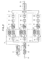
- Fig.3 is a block diagram showing a receiver of the invention.
- the received signal input being from input terminal 30 is supplied to a timing/frequency offset estimating section 31 and a delaying section 32.
- Timing/frequency offset estimating section 31 estimates the symbol timing and the frequency offset.
- Delaying section 32 in Fig.3 delays the received signal by the time required for the estimation of the timing and frequency offset to supply the signal to a frequency compensator 33.
- Frequency compensator 33 compensates frequency offset based on the estimated frequency offset determined in timing/frequency offset estimating section 31.
- the compensation of the frequency offset here is performed for only the offset of fixed frequency between the transmitter and receiver.
- the received signal after frequency offset compensation is input to n number of band-pass filters 40, 41 and 42 so that the signal is divided into band ranges of n parts.
- the frequency distribution characteristic of each band-pass filter is shown in Fig.4.
- the band of each band-pass filter is set around a level equal to or lower than the coherence band width of the propagation path.
- the divided signals are input to variation estimating sections 43, 44 and 45 as well as delaying sections 46, 47 and 48.
- the variation estimating section estimates time-dependent variations due to the phasing propagation path.
- Each delaying section delays the signal by the time required for the estimation and input the signal to variation compensator 51, 52 and 53, respectively.
- Variation compensators 51, 52 and 53 compensate time-dependent variations in the signals based on the estimated variations due to the propagation path.
- the compensated signals are supplied to discrete Fourier transformers 61, 62 and 63 respectively, where the signal is divided into subchannel signals.
- the subchannel signals are converted into serial data in parallel-to-serial converter 64, 65 and 66 and the converted data is then multiplexed in a multiplexing circuit 37.
- the multiplexed signal obtained from multiplexing circuit 37 is determined and demodulated in a demodulator 38 so as to reproduce the transmitted data.
- the data stream is output from an output terminal 39.
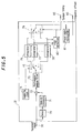
- Fig.5 is a block diagram showing the timing/frequency offset estimating section used in the above embodiment.
- the received signal being input from input terminal 30 is delayed by an observation time t s in a delaying section 70.
- the output signal from delaying section 70 is supplied to a complex conjugate calculating section 71 where the complex conjugate signal is calculated.
- the output signal from complex conjugate calculating section 71 as well as the received signal being input from input terminal 30 is input to complex multiplier 72.
- the output signal from the multiplier is input to a rectangular window filter 73 having a rectangular impulse response of width ⁇ .
- the output from rectangular window filter 73 is supplied to a distributing switch 75.
- the output signal from a sampling clock 74 is also input to distributing switch 75, where the output from rectangular filter 73 is distributed to n number of integrators 76, 77 and 78 based on the clock timing.
- Each integrator calculates the integral of the input signal taken across the M symbol intervals of the multi-frequency quadrature signal. By this calculation, a likelihood function represented by formula (1) is determined.
- t samp represents a sampling period
- t s an observation interval length
- ⁇ a guard interval length
- Each integrator output is input to peak detector 80, where it is determined which integrator output has the greatest amplitude.
- the output from peak detector 80 is output from a symbol timing signal output terminal 82.
- phase angle calculating section 81 the phases of the output signals from integrators 76, 77 and 78 are calculated.
- the output signal from phase angle calculating section 81 is output from a frequency offset estimate value output terminal 83.
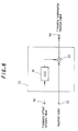
- Fig.6 shows the configuration of frequency offset compensator 33 used in this invention.
- the frequency offset estimate value is supplied from a frequency offset estimate value input terminal 90 to a voltage controlled oscillator 91, where a sinusoidal signal having a frequency in conformity with the frequency offset is generated.
- the oscillator output signal and the received signal being input from a received signal input terminal 92 are input together to a multiplier 93.
- Multiplier 93 performs complex multiplication and compensates its frequency offset.
- the output from multiplier 93 is output from a frequency compensated received signal output terminal 94.
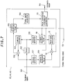
- Fig.7 shows the configuration of propagation path variation estimating sections 43, 44 and 45 used in this invention.
- the received signal being input from a received signal input terminal 100 is supplied to delaying section 102 where the signal is delayed by time t s .
- the delaying section output is supplied to a complex conjugate calculating section 103 where its complex conjugate signal is calculated.
- the output signal from complex conjugate calculating section 103 is being input together with the input signal from received signal input terminal 100 to a multiplier 104, and complex multiplication is made.
- the output from multiplier 104 is input to an integral discharge filter 105, where the integral of the output is calculated based on the symbol timing being input from a symbol timing signal input terminal 101. Further, the integral discharge filter output signal is supplied to a phase angle calculating section 106.
- the output signal from phase angle calculating section 106 is a variation in phase across one symbol interval shown in formula (2).
- the received signal being input from received signal input terminal 100 and the output from delaying section 102 are also supplied to envelop detectors 107 and 108 respectively, where the amplitude of the received signal is calculated.
- the outputs from envelop detectors 107 and 108 are input to integral discharge filters 109 and 110 respectively, where the integral of the signal is calculated based on the symbol timing being input from symbol timing signal input terminal 101. Further, the output from integral discharge filter 110 is supplied to a reciprocal calculating section 111, where the reciprocal is calculated. The output from integral discharge filter 110 and the output from reciprocal calculating section 111 are supplied to a multiplier 112.
- the output from multiplier 112 is the estimate value of the variation ratio of the amplitude across one symbol interval, calculated by formula (3):
- the output from multiplier 112 and the output signal from phase angle calculating section 106 are input to a polar coordinate-to-rectangular coordinate converter 113, where the signal is converted into a complex number representing variation in amplitude and phase and this will be output from an estimate value output terminal 114.
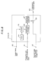
- Fig.8 shows a propagating path variation compensating circuit used in this invention.
- the timing signal being input from symbol timing signal input terminal 120 is supplied together with a clock pulse signal generated from a sampling clock oscillator 124 to a counter 125.
- a timing signal which will be reset by the symbol timing signal is generated.
- the output signal from counter 125 is input to interpolation calculating section 126.
- the estimate value of the propagation path variation during interval t s supplied from a propagation path variation estimate signal input terminal 121 is supplied to interpolation calculating section 126.
- interpolation calculating section 126 the interpolating calculation is made following formula (4), so as to determine the estimate value of the variation in amplitude and phase caused by the propagation path within symbol interval.
- the estimate of the propagation path variation determined by formula (3) is input to a reciprocal calculating section 127 where its reciprocal is determined.
- the output signal from reciprocal calculating section 127 is input together with the received signal from a received signal input terminal 122 to a multiplier 128 and multiplication is made.
- the multiplier output signal is output from a compensated signal output terminal 123.
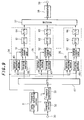
- Fig.9 is another embodiment of the invention and its operation will be described hereinbelow using this figure.
- the received signal being input from input terminal 30 is supplied to timing/frequency offset estimating section 31 and delaying section 32.
- Timing/frequency offset estimating section 31 estimates the symbol timing and the frequency offset.
- Delaying section 32 in Fig.9 delays the received signal by the time required for the estimation of the timing and frequency offset to supply it to frequency compensator 33.
- Frequency compensator 33 compensates the frequency offset based on the estimate of the frequency offset estimated in timing/frequency offset estimating section 31.
- the compensation of the frequency offset here is performed for only the offset of fixed frequency between the transmitter and receiver.
- the received signal with its frequency offset compensated is supplied to a DFT 167 and divided into n number of bands.
- the signals divided by DFT 167 are input to variation estimating sections 43, 44 and 45 as well as delaying sections 46, 47 and 48.
- the variation estimating section estimates time-dependent variations in the phasing propagation path.
- the delaying sections delay the signals by the time required for the estimation and input the signals to variation compensators 51, 52 and 53, respectively.
- Variation compensators 51, 52 and 53 compensate the time-dependent variations in the signals based on the estimated variations in the propagation path.
- the signal after compensation is divided into subchannel signals in discrete Fourier transformers 61, 62 and 63, and then these signals are converted into serial data in parallel-to-serial converters 64, 65 and 66, and then multiplexed in multiplexing circuit 37.
- the multiplexed signal obtained from multiplexing circuit 37 is determined and demodulated in a demodulator 38 so as to reproduce the transmitted data.
- the data stream is output from output terminal 39.
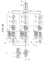
- Fig.10 shows another mode of the embodiment of the invention. Referring to Fig.10, the operation will be descried hereinbelow.
- the received signal being input from input terminal 30 is supplied to frequency compensator 33.
- the output from frequency compensator 33 is input to timing/frequency offset estimating section 31 and band-pass filters (BPF) 40, 41 and 42.
- BPF band-pass filters
- Timing/frequency offset estimating section 31 estimates symbol timing and frequency offset.
- Frequency compensator 33 compensates frequency offset based on the estimate value of frequency offset estimated in timing/frequency offset estimating section 31 (feedback technique).
- the compensation of the frequency offset here is performed for only the offset of fixed frequency between the transmitter and receiver.
- the operation following are the same as in the embodiment shown in Fig.3.
- the frequency offset section can be performed based on either feed forward or feedback technique.
- this invention contributes to suppress the degradation of the transmission characteristics due to a propagation path variation.
Landscapes
- Engineering & Computer Science (AREA)
- Computer Networks & Wireless Communication (AREA)
- Signal Processing (AREA)
- Power Engineering (AREA)
- Digital Transmission Methods That Use Modulated Carrier Waves (AREA)
- Cable Transmission Systems, Equalization Of Radio And Reduction Of Echo (AREA)
Applications Claiming Priority (3)
| Application Number | Priority Date | Filing Date | Title |
|---|---|---|---|
| JP34320496A JP3431785B2 (ja) | 1996-12-24 | 1996-12-24 | 直交周波数多重変調信号復調装置 |
| JP34320496 | 1996-12-24 | ||
| JP343204/96 | 1996-12-24 |
Publications (3)
| Publication Number | Publication Date |
|---|---|
| EP0851642A2 true EP0851642A2 (de) | 1998-07-01 |
| EP0851642A3 EP0851642A3 (de) | 2000-08-23 |
| EP0851642B1 EP0851642B1 (de) | 2006-09-13 |
Family
ID=18359727
Family Applications (1)
| Application Number | Title | Priority Date | Filing Date |
|---|---|---|---|
| EP97310598A Expired - Lifetime EP0851642B1 (de) | 1996-12-24 | 1997-12-24 | Mehrträgerempfänger mit Ausgleich von Frequenzverschiebungen und von frequenzabhängigen Verzerrungen |
Country Status (5)
| Country | Link |
|---|---|
| US (1) | US6058145A (de) |
| EP (1) | EP0851642B1 (de) |
| JP (1) | JP3431785B2 (de) |
| DE (1) | DE69736659T2 (de) |
| ES (1) | ES2270450T3 (de) |
Cited By (5)
| Publication number | Priority date | Publication date | Assignee | Title |
|---|---|---|---|---|
| GB2347285A (en) * | 1999-02-24 | 2000-08-30 | Motorola Ltd | Method and apparatus for frequency synchronisation in a digital radio communications system |
| GB2366145A (en) * | 2000-07-05 | 2002-02-27 | Fuji Television Network Inc | Underground broadcasting system |
| GB2373973A (en) * | 2001-03-30 | 2002-10-02 | Toshiba Res Europ Ltd | Adaptive OFDM receiver where sets of sub-carriers which are coherent are grouped into sub-bands and a single weight is calculated for each sub-band |
| EP1071227A3 (de) * | 1999-07-21 | 2003-02-19 | NTT DoCoMo, Inc. | CDMA-Empfangsvorrichtung und Leistungsmessvorrichtung des empfangenen Signals in einem mobilen CDMA-Kommunikationssystem |
| EP2720426A1 (de) * | 2012-10-09 | 2014-04-16 | Mitsubishi Electric R&D Centre Europe B.V. | Verfahren und Vorrichtung zur Korrektur einer Frequenzverschiebung bei empfangenen Symbolen |
Families Citing this family (20)
| Publication number | Priority date | Publication date | Assignee | Title |
|---|---|---|---|---|
| JP3507683B2 (ja) * | 1998-01-09 | 2004-03-15 | 株式会社エヌ・ティ・ティ・ドコモ | 並列伝送方法 |
| US6618352B1 (en) | 1998-05-26 | 2003-09-09 | Matsushita Electric Industrial Co., Ltd. | Modulator, demodulator, and transmission system for use in OFDM transmission |
| US6177835B1 (en) * | 1998-07-31 | 2001-01-23 | The United States Of America As Represented By The Administrator Of The National Aeronautics And Space Administration | Method and apparatus for high data rate demodulation |
| WO2001001590A1 (fr) * | 1999-06-29 | 2001-01-04 | Mitsubishi Denki Kabushiki Kaisha | Circuit de commande de frequence automatique et demodulateur |
| JP3676991B2 (ja) | 2001-07-05 | 2005-07-27 | 松下電器産業株式会社 | 無線通信装置及び無線通信方法 |
| US20040229127A1 (en) | 2003-05-13 | 2004-11-18 | Wensley C. Glen | Polyimide matrix electrolyte |
| US20040253520A1 (en) | 2003-05-13 | 2004-12-16 | Wensley C. Glen | Polyimide matrix electrolyte and improved batteries therefrom |
| US6936377B2 (en) | 2003-05-13 | 2005-08-30 | C. Glen Wensley | Card with embedded IC and electrochemical cell |
| US7390336B2 (en) | 2003-07-29 | 2008-06-24 | Solicore, Inc. | Polyimide-based lithium metal battery |
| EP1787344B1 (de) | 2004-07-22 | 2017-02-22 | BrightVolt, Inc. | Verbesserter batterielaschen- und kapselungsentwurf |
| KR100707437B1 (ko) | 2005-03-03 | 2007-04-13 | 엘지전자 주식회사 | 다중경로 수신신호의 지연을 보상하는 이동통신 시스템 |
| US20070064740A1 (en) * | 2005-09-19 | 2007-03-22 | Shai Waxman | Device, system and method of clock synchronization |
| KR101100791B1 (ko) * | 2006-10-16 | 2012-01-02 | 닛본 덴끼 가부시끼가이샤 | 수신 방법 및 수신 장치 |
| JP4516591B2 (ja) * | 2007-11-28 | 2010-08-04 | 日本電信電話株式会社 | 周波数多重信号受信装置 |
| JP2010045672A (ja) * | 2008-08-15 | 2010-02-25 | Nippon Telegr & Teleph Corp <Ntt> | 信号受信装置及び方法 |
| JP4940222B2 (ja) * | 2008-11-20 | 2012-05-30 | 日本電信電話株式会社 | 信号受信装置及び方法 |
| US8655282B2 (en) * | 2010-10-29 | 2014-02-18 | Qualcomm Incorporated | Multiple signal transformation in wireless receivers |
| CN109859760A (zh) * | 2019-02-19 | 2019-06-07 | 成都富王科技有限公司 | 基于深度学习的电话机器人语音识别结果校正方法 |
| CN119213686A (zh) * | 2022-04-13 | 2024-12-27 | 斯塔西拉知识产权控股公司 | 通过与数控低频补偿信号混频的参考时钟频率校正 |
| US12267201B1 (en) * | 2024-10-15 | 2025-04-01 | HaiLa Technologies Inc. | Systems and methods for estimating symbol timing in received data frames |
Family Cites Families (7)
| Publication number | Priority date | Publication date | Assignee | Title |
|---|---|---|---|---|
| JPS6052147A (ja) * | 1983-09-01 | 1985-03-25 | Nec Corp | タイミング同期方式 |
| JP3041175B2 (ja) * | 1993-11-12 | 2000-05-15 | 株式会社東芝 | Ofdm同期復調回路 |
| JP3074103B2 (ja) * | 1993-11-16 | 2000-08-07 | 株式会社東芝 | Ofdm同期復調回路 |
| JP2655108B2 (ja) * | 1994-12-12 | 1997-09-17 | 日本電気株式会社 | Cdma送受信装置 |
| JP3130752B2 (ja) * | 1995-02-24 | 2001-01-31 | 株式会社東芝 | Ofdm伝送受信方式及び送受信装置 |
| US5680421A (en) * | 1995-02-27 | 1997-10-21 | Oki Electric Industry Co., Ltd. | Frame synchronization apparatus |
| DE69634027T2 (de) * | 1995-08-14 | 2005-12-22 | Nippon Telegraph And Telephone Corp. | Akustischer Teilband-Echokompensator |
-
1996
- 1996-12-24 JP JP34320496A patent/JP3431785B2/ja not_active Expired - Lifetime
-
1997
- 1997-12-11 US US08/988,934 patent/US6058145A/en not_active Expired - Lifetime
- 1997-12-24 EP EP97310598A patent/EP0851642B1/de not_active Expired - Lifetime
- 1997-12-24 DE DE69736659T patent/DE69736659T2/de not_active Expired - Lifetime
- 1997-12-24 ES ES97310598T patent/ES2270450T3/es not_active Expired - Lifetime
Cited By (14)
| Publication number | Priority date | Publication date | Assignee | Title |
|---|---|---|---|---|
| GB2347285B (en) * | 1999-02-24 | 2001-03-21 | Motorola Ltd | Method and apparatus for frequency synchronisation in a digital radio communications system |
| GB2347285A (en) * | 1999-02-24 | 2000-08-30 | Motorola Ltd | Method and apparatus for frequency synchronisation in a digital radio communications system |
| US6999427B1 (en) | 1999-07-21 | 2006-02-14 | Ntt Docomo, Inc. | CDMA reception apparatus and received signal power measuring apparatus in CDMA mobile communication system |
| EP1071227A3 (de) * | 1999-07-21 | 2003-02-19 | NTT DoCoMo, Inc. | CDMA-Empfangsvorrichtung und Leistungsmessvorrichtung des empfangenen Signals in einem mobilen CDMA-Kommunikationssystem |
| US7649859B2 (en) | 1999-07-21 | 2010-01-19 | Ntt Docomo, Inc. | Channel identifier assigning method and mobile communications system |
| SG101425A1 (en) * | 1999-07-21 | 2004-01-30 | Ntt Docomo Inc | Cdma reception apparatus and received signal power measuring apparatus in cdma mobile communication system |
| EP1460777A3 (de) * | 1999-07-21 | 2005-03-30 | NTT DoCoMo, Inc. | CDMA-Empfangsvorrichtung und Leistungsmessverfahren des empfangenen Signals in einem mobilen CDMA-Kommunikationssystem |
| GB2366145A (en) * | 2000-07-05 | 2002-02-27 | Fuji Television Network Inc | Underground broadcasting system |
| GB2366145B (en) * | 2000-07-05 | 2002-10-30 | Fuji Television Network Inc | Underground broadcasting system |
| GB2373973A (en) * | 2001-03-30 | 2002-10-02 | Toshiba Res Europ Ltd | Adaptive OFDM receiver where sets of sub-carriers which are coherent are grouped into sub-bands and a single weight is calculated for each sub-band |
| GB2373973B (en) * | 2001-03-30 | 2003-06-11 | Toshiba Res Europ Ltd | Adaptive antenna |
| EP2720426A1 (de) * | 2012-10-09 | 2014-04-16 | Mitsubishi Electric R&D Centre Europe B.V. | Verfahren und Vorrichtung zur Korrektur einer Frequenzverschiebung bei empfangenen Symbolen |
| WO2014057742A1 (en) * | 2012-10-09 | 2014-04-17 | Mitsubishi Electric Corporation | Method, device and computer program for correcting a frequency shift on symbols received by a receiver |
| US9735997B2 (en) | 2012-10-09 | 2017-08-15 | Mitsubishi Electric Corporation | Method, device and computer program for correcting a frequency shift on symbols received by a receiver |
Also Published As
| Publication number | Publication date |
|---|---|
| DE69736659T2 (de) | 2007-09-13 |
| EP0851642A3 (de) | 2000-08-23 |
| ES2270450T3 (es) | 2007-04-01 |
| JP3431785B2 (ja) | 2003-07-28 |
| DE69736659D1 (de) | 2006-10-26 |
| EP0851642B1 (de) | 2006-09-13 |
| JPH10190609A (ja) | 1998-07-21 |
| US6058145A (en) | 2000-05-02 |
Similar Documents
| Publication | Publication Date | Title |
|---|---|---|
| US6058145A (en) | Method of demodulating a multi-frequency quadrature modulated signal | |
| EP0839423B1 (de) | Pulsformung für mehrträgermodulation | |
| RU2454808C2 (ru) | Схема модуляции на нескольких несущих, а также передающее устройство и приемное устройство, использующие указанную схему | |
| CN1980217B (zh) | 发送方法、发送装置、接收方法、接收装置 | |
| EP0929172B1 (de) | System zur Mehrträgermodulation, mit veränderbaren Symbolgeschwindigkeiten | |
| US7009931B2 (en) | Synchronization in a multiple-input/multiple-output (MIMO) orthogonal frequency division multiplexing (OFDM) system for wireless applications | |
| EP0683576B1 (de) | Digitales OFDM-Rundfunksystem, sowie Übertragungs- und Empfangsvorrichtung für Digitalrundfunk | |
| EP0955754B1 (de) | Verfahren un Anordnung zum Erreichen und Aufrechterhalten der Symbolsynchronisierung in einem OFDM-Übertragungssystem | |
| US5802117A (en) | Method and apparatus for joint frequency offset and timing estimation of a multicarrier modulation system | |
| EP0901256B1 (de) | Übertragungssystem für OFDM-Signalen mit optimierter Synchronisation | |
| EP1108295B1 (de) | Verfahren zum Aufbau einer Trainingsfolge | |
| US6363131B1 (en) | Method and apparatus for joint timing synchronization and frequency offset estimation | |
| US9596118B2 (en) | FBMC receiver using a method for synchronization in a frequency domain | |
| Hazy et al. | Synchronization of OFDM systems over frequency selective fading channels | |
| JPH08237218A (ja) | 周波数同調回路からなる直交周波数分割多重信号用の送信機及び受信機 | |
| EP1039713A2 (de) | Verringerung von Verzögerung in Mehrträgerempfängern | |
| KR100213100B1 (ko) | Ofdm 전송 신호의 주파수 오류 정정기와 그 방법 | |
| JP3609937B2 (ja) | 受信機 | |
| JP2000022660A (ja) | ディジタル通信装置 | |
| JPH07154129A (ja) | Lms方式のアダプティブアレイアンテナ装置 | |
| JP2003152673A (ja) | 直交周波数多重変調信号復調方法 | |
| JP3514965B2 (ja) | 受信装置 | |
| JP2004201338A (ja) | 送信機および伝送方法 | |
| USRE43829E1 (en) | Transmission system for OFDM-signals with optimized synchronization |
Legal Events
| Date | Code | Title | Description |
|---|---|---|---|
| PUAI | Public reference made under article 153(3) epc to a published international application that has entered the european phase |
Free format text: ORIGINAL CODE: 0009012 |
|
| AK | Designated contracting states |
Kind code of ref document: A2 Designated state(s): DE ES FR GB IT |
|
| AX | Request for extension of the european patent |
Free format text: AL;LT;LV;MK;RO;SI |
|
| PUAL | Search report despatched |
Free format text: ORIGINAL CODE: 0009013 |
|
| AK | Designated contracting states |
Kind code of ref document: A3 Designated state(s): AT BE CH DE DK ES FI FR GB GR IE IT LI LU MC NL PT SE |
|
| AX | Request for extension of the european patent |
Free format text: AL;LT;LV;MK;RO;SI |
|
| RIC1 | Information provided on ipc code assigned before grant |
Free format text: 7H 04L 27/26 A, 7H 04L 25/03 B |
|
| RIN1 | Information on inventor provided before grant (corrected) |
Inventor name: KAWABE, TAKESHI Inventor name: OKADA, MINORU Inventor name: KOMAKI, SHOZO |
|
| 17P | Request for examination filed |
Effective date: 20001107 |
|
| AKX | Designation fees paid |
Free format text: DE ES FR GB IT |
|
| 17Q | First examination report despatched |
Effective date: 20040310 |
|
| GRAP | Despatch of communication of intention to grant a patent |
Free format text: ORIGINAL CODE: EPIDOSNIGR1 |
|
| GRAS | Grant fee paid |
Free format text: ORIGINAL CODE: EPIDOSNIGR3 |
|
| GRAA | (expected) grant |
Free format text: ORIGINAL CODE: 0009210 |
|
| AK | Designated contracting states |
Kind code of ref document: B1 Designated state(s): DE ES FR GB IT |
|
| REG | Reference to a national code |
Ref country code: GB Ref legal event code: FG4D |
|
| REF | Corresponds to: |
Ref document number: 69736659 Country of ref document: DE Date of ref document: 20061026 Kind code of ref document: P |
|
| REG | Reference to a national code |
Ref country code: ES Ref legal event code: FG2A Ref document number: 2270450 Country of ref document: ES Kind code of ref document: T3 |
|
| ET | Fr: translation filed | ||
| PLBE | No opposition filed within time limit |
Free format text: ORIGINAL CODE: 0009261 |
|
| STAA | Information on the status of an ep patent application or granted ep patent |
Free format text: STATUS: NO OPPOSITION FILED WITHIN TIME LIMIT |
|
| 26N | No opposition filed |
Effective date: 20070614 |
|
| REG | Reference to a national code |
Ref country code: FR Ref legal event code: PLFP Year of fee payment: 19 |
|
| PGFP | Annual fee paid to national office [announced via postgrant information from national office to epo] |
Ref country code: DE Payment date: 20151211 Year of fee payment: 19 Ref country code: GB Payment date: 20151221 Year of fee payment: 19 |
|
| PGFP | Annual fee paid to national office [announced via postgrant information from national office to epo] |
Ref country code: ES Payment date: 20151214 Year of fee payment: 19 Ref country code: FR Payment date: 20151221 Year of fee payment: 19 |
|
| PGFP | Annual fee paid to national office [announced via postgrant information from national office to epo] |
Ref country code: IT Payment date: 20151228 Year of fee payment: 19 |
|
| REG | Reference to a national code |
Ref country code: DE Ref legal event code: R119 Ref document number: 69736659 Country of ref document: DE |
|
| GBPC | Gb: european patent ceased through non-payment of renewal fee |
Effective date: 20161224 |
|
| REG | Reference to a national code |
Ref country code: FR Ref legal event code: ST Effective date: 20170831 |
|
| PG25 | Lapsed in a contracting state [announced via postgrant information from national office to epo] |
Ref country code: IT Free format text: LAPSE BECAUSE OF NON-PAYMENT OF DUE FEES Effective date: 20161224 Ref country code: FR Free format text: LAPSE BECAUSE OF NON-PAYMENT OF DUE FEES Effective date: 20170102 |
|
| PG25 | Lapsed in a contracting state [announced via postgrant information from national office to epo] |
Ref country code: GB Free format text: LAPSE BECAUSE OF NON-PAYMENT OF DUE FEES Effective date: 20161224 Ref country code: DE Free format text: LAPSE BECAUSE OF NON-PAYMENT OF DUE FEES Effective date: 20170701 |
|
| REG | Reference to a national code |
Ref country code: ES Ref legal event code: FD2A Effective date: 20180507 |
|
| PG25 | Lapsed in a contracting state [announced via postgrant information from national office to epo] |
Ref country code: ES Free format text: LAPSE BECAUSE OF FAILURE TO SUBMIT A TRANSLATION OF THE DESCRIPTION OR TO PAY THE FEE WITHIN THE PRESCRIBED TIME-LIMIT Effective date: 20060913 |
|
| PG25 | Lapsed in a contracting state [announced via postgrant information from national office to epo] |
Ref country code: ES Free format text: LAPSE BECAUSE OF FAILURE TO SUBMIT A TRANSLATION OF THE DESCRIPTION OR TO PAY THE FEE WITHIN THE PRESCRIBED TIME-LIMIT Effective date: 20161225 |