EP0852410A2 - Dispositif de circuit électrique - Google Patents
Dispositif de circuit électrique Download PDFInfo
- Publication number
- EP0852410A2 EP0852410A2 EP97122985A EP97122985A EP0852410A2 EP 0852410 A2 EP0852410 A2 EP 0852410A2 EP 97122985 A EP97122985 A EP 97122985A EP 97122985 A EP97122985 A EP 97122985A EP 0852410 A2 EP0852410 A2 EP 0852410A2
- Authority
- EP
- European Patent Office
- Prior art keywords
- conductors
- conductor
- electrical
- circuit arrangement
- facing
- Prior art date
- Legal status (The legal status is an assumption and is not a legal conclusion. Google has not performed a legal analysis and makes no representation as to the accuracy of the status listed.)
- Withdrawn
Links
- 239000004020 conductor Substances 0.000 claims abstract description 139
- 230000008878 coupling Effects 0.000 claims abstract description 23
- 238000010168 coupling process Methods 0.000 claims abstract description 23
- 238000005859 coupling reaction Methods 0.000 claims abstract description 23
- 230000005684 electric field Effects 0.000 description 18
- 238000010586 diagram Methods 0.000 description 7
- 238000003491 array Methods 0.000 description 2
- 238000003780 insertion Methods 0.000 description 2
- 230000037431 insertion Effects 0.000 description 2
- 230000013011 mating Effects 0.000 description 2
- 230000009286 beneficial effect Effects 0.000 description 1
- 230000000295 complement effect Effects 0.000 description 1
- 238000010276 construction Methods 0.000 description 1
- 239000000463 material Substances 0.000 description 1
- 238000000034 method Methods 0.000 description 1
- 239000002991 molded plastic Substances 0.000 description 1
- 239000004033 plastic Substances 0.000 description 1
- 239000007787 solid Substances 0.000 description 1
Images



Classifications
-
- H—ELECTRICITY
- H01—ELECTRIC ELEMENTS
- H01R—ELECTRICALLY-CONDUCTIVE CONNECTIONS; STRUCTURAL ASSOCIATIONS OF A PLURALITY OF MUTUALLY-INSULATED ELECTRICAL CONNECTING ELEMENTS; COUPLING DEVICES; CURRENT COLLECTORS
- H01R13/00—Details of coupling devices of the kinds covered by groups H01R12/70 or H01R24/00 - H01R33/00
- H01R13/646—Details of coupling devices of the kinds covered by groups H01R12/70 or H01R24/00 - H01R33/00 specially adapted for high-frequency, e.g. structures providing an impedance match or phase match
- H01R13/6461—Means for preventing cross-talk
- H01R13/6464—Means for preventing cross-talk by adding capacitive elements
-
- H—ELECTRICITY
- H01—ELECTRIC ELEMENTS
- H01R—ELECTRICALLY-CONDUCTIVE CONNECTIONS; STRUCTURAL ASSOCIATIONS OF A PLURALITY OF MUTUALLY-INSULATED ELECTRICAL CONNECTING ELEMENTS; COUPLING DEVICES; CURRENT COLLECTORS
- H01R13/00—Details of coupling devices of the kinds covered by groups H01R12/70 or H01R24/00 - H01R33/00
- H01R13/646—Details of coupling devices of the kinds covered by groups H01R12/70 or H01R24/00 - H01R33/00 specially adapted for high-frequency, e.g. structures providing an impedance match or phase match
- H01R13/6473—Impedance matching
- H01R13/6477—Impedance matching by variation of dielectric properties
Definitions
- This invention generally relates to the art of electrical conductors or terminals and, particularly, to an electrical circuit arrangement for controlling the electrical characteristics between adjacent conductors.
- crosstalk horizontal capacitance
- An object, therefore, of the invention is to provide an electrical circuit arrangement wherein the electrical characteristics, such as the crosstalk (horizontal capacitance) between selected conductors in the circuit arrangement, is different.
- an electrical circuit arrangement includes at least three adjacent spaced-apart, elongate parallel conductors including a middle conductor having two oppositely facing surfaces.
- a left conductor has a surface facing the first surface of the middle conductor to define a first electrical coupling.
- a right conductor has a surface facing the second surface of the middle conductor to define a second electrical coupling.
- the invention contemplates that the shape of the facing surfaces between the left conductor and the middle conductor be different from the shape of the facing surfaces between the right conductor and the middle conductor. Therefore, the electrical characteristics of the first electrical coupling is different from the electrical characteristics of the second electrical coupling.
- the facing surfaces between one of the left or right conductors and the middle conductor are narrower than the facing surfaces between the other of the left or right conductors and the middle conductor.
- the narrower facing surfaces cause less crosstalk (horizontal capacitance) than the wider surfaces.
- the facing surfaces between at least one of the left or right conductors and the middle conductor are pointed.
- the facing surfaces between at least one of the left or right conductors and the middle conductor are generally flat.
- the facing surfaces between at least one of the left or right conductors and the middle conductor are rounded.
- the concepts of the invention comprising the unique electrical circuit arrangement are shown herein in one embodiment wherein the conductors are in a generally parallel array in an electrical cable.
- the conductors comprise terminals in an electrical connector.
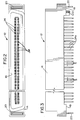
- an electrical connector 12 includes an elongated dielectric housing 14, such as of molded plastic material or the like.
- the housing has a receptacle 16 defining a mating face of the connector for mating with a complementary connector, such as a plug connector inserted into receptacle 16.
- the opposite face 18 of the housing is adapted for surface mounting on a printed circuit board.
- Figure 3 shows that a pair of boardlocks 20 may depend from housing 14 for insertion into appropriate mounting holes in the printed circuit board.
- a polarizing peg 22 also may depend from housing 14 for inserting into a polarizing hole in the circuit board.
- the housing mounts a plurality of terminals 24 which, as best seen in Figure 2, are arranged in two rows lengthwise of the housing.
- the terminals have tails portions 24a, also in two rows and depending from surface 18 of the housing for insertion into appropriate holes in the printed circuit board.
- the tails typically are soldered to circuit traces on the board and/or in the holes.
- connector 12 is generally conventional.
- Figure 4 shows a generally flat electrical cable, generally designated 26, which includes a dielectric 28 surrounding three pairs of conductors 30a,30b; 32a,32b and 34a,34b. Therefore, conductors 30a and 30b comprise a left-hand pair, conductors 32a and 32b comprise a center pair and conductors 34a and 34b comprise a right-hand pair. It can be seen that the facing surfaces 36 between the conductors in each pair are generally flat. However, the facing surfaces 38 between the conductors of two adjacent pairs are pointed. Of course, this results in the facing flat surfaces 36 forming a greater interface area than the opposing pointed surfaces 38.
- this diagram shows a section through three pairs of the terminal tails 24a in each of the two rows of terminals in connector 12 as might be taken along line 5-5 of Figure 3.
- the terminal tails 24a in Figure 5 have been numbered corresponding to the conductors in Figure 4 so that the depiction in Figure 5 includes two rows of conductors (terminal tails) with three pairs of conductors (terminal tails) in each row. Therefore, as with the conductors in Figure 4, the conductors or terminal tails in each of the top and bottom rows in Figure 5 include a left-hand pair 30a,30b; a center pair 32a,32b and a right-hand pair 34a,34b.
- the facing surfaces 36 between the conductors in each pair are relatively large and flat, whereas the facing surfaces 38 between the conductors of adjacent pairs are relatively narrow and pointed.
- Figures 5 and 6 represent computer generated diagrams of the electrical fields between the conductors in connector 12 (Figs. 1-3) and cable 26 (Fig. 4), respectively.
- Figure 5 corresponds to the terminal tails 24a of connector 12
- Figure 6 corresponds to the conductors of cable 26 in Figure 4.
- capacitance is proportional to the amount of energy stored in the electrical field in and around a particular structure (e.g. conductor).
- capacitance is proportional to the amount of energy stored in the electric field due to the voltage differential across a dielectric whether it be plastic or air.
- U e 1 ⁇ 2Cv 2
- U e is the energy stored in the electric field
- C is the capacitance
- v is the voltage across the dielectric.
- solid field lines 40 represent the highest electrical field magnitude (volts).
- Dotted field lines 42 represent the lowest electric field magnitude.
- Dashed field lines 44 represent the electric field of intermediate magnitude.
- capacitance is proportional to the amount of energy stored in the electric field in and around the conductors, the capacitance is proportional to or represents the "coupling" between the conductors. The capacitance also is related to the crosstalk between the conductors.
- Figure 7 shows another generally flat electrical cable, generally designated 26', which includes a dielectric 28' surrounding three pairs of conductors 30a',30b'; 32a', 32b' and 34a',34b'.
- Cable 26' is similar to cable 26 (Fig. 4) except that opposing flat surfaces 36 between the conductors of each pair and opposing pointed surfaces 38 between the conductors of adjacent pairs are formed on generally flat or planar conductors versus the curved conductors shown in Figure 4.
- Figures 8-10 simply show further examples of reducing the area of the facing surfaces of conductors versus the pointed surfaces 38 in the embodiments described hereinbefore. In all of Figures 8-10, the conductors are embedded in a dielectric 28.
- conductor 50 has a rounded edge 50a to reduce the surface area which would face an adjacent conductor.
- conductor 52 has a quarter-round surface 52a which still reduces the edge surface area.
- conductor 54 has a flat surface 54a, but the flat surface is considerably narrower than the flat surfaces 36 described above, because the remainder of the edge 54b of the conductor is tapered or angled back toward the adjacent side of the conductor.
- the capacitance coupling between the adjacent couplings is minimized which, in appropriate applications, is effective to also minimize the crosstalk between the adjacent conductors.
- Figure 11 is an illustration which shows an electrical circuit arrangement, generally designated 58, in which not only can the crosstalk between adjacent conductors in any given row of conductors (i.e. Figs. 5 and 6) be controlled, but the crosstalk or capacitive coupling between the conductors in adjacent rows also can be controlled.
- Figure 11 shows three pairs of conductors 60a,60b; 62a,62b and 64a,64b in each of two rows, generally designated 66 and 68.
- larger flat surfaces 36 between any two adjacent conductors will create an electric field of a higher magnitude and, therefore, a higher coupling, than the field between facing pointed surfaces 38.
- the surfaces 70 between conductors 60a, between conductors 60b, between conductors 62a, between conductors 64a and between conductors 64b in the two rows 66 and 68 are rounded in comparison to the larger flat opposing surfaces 72 between conductors 62b in the two rows. Therefore, larger flat surfaces 72 between adjacent conductors 62b in the two rows will create a higher electric field magnitude and, therefore, a higher capacitive coupling, than either the opposing or facing pointed surfaces 38 or the opposing, facing rounded surfaces 70 between any other two conductors in either row or in the adjacent conductors in both rows.
Landscapes
- Coupling Device And Connection With Printed Circuit (AREA)
- Details Of Connecting Devices For Male And Female Coupling (AREA)
- Insulated Conductors (AREA)
Applications Claiming Priority (2)
| Application Number | Priority Date | Filing Date | Title |
|---|---|---|---|
| US778461 | 1997-01-03 | ||
| US08/778,461 US5834700A (en) | 1997-01-03 | 1997-01-03 | Electrical circuit arrangement |
Publications (2)
| Publication Number | Publication Date |
|---|---|
| EP0852410A2 true EP0852410A2 (fr) | 1998-07-08 |
| EP0852410A3 EP0852410A3 (fr) | 1999-07-21 |
Family
ID=25113425
Family Applications (1)
| Application Number | Title | Priority Date | Filing Date |
|---|---|---|---|
| EP97122985A Withdrawn EP0852410A3 (fr) | 1997-01-03 | 1997-12-30 | Dispositif de circuit électrique |
Country Status (3)
| Country | Link |
|---|---|
| US (1) | US5834700A (fr) |
| EP (1) | EP0852410A3 (fr) |
| JP (1) | JP3104172B2 (fr) |
Cited By (1)
| Publication number | Priority date | Publication date | Assignee | Title |
|---|---|---|---|---|
| GB2399953A (en) * | 2003-02-25 | 2004-09-29 | Compal Electronics Inc | Serial advanced technology attachment connector |
Families Citing this family (1)
| Publication number | Priority date | Publication date | Assignee | Title |
|---|---|---|---|---|
| US9577305B2 (en) * | 2011-08-12 | 2017-02-21 | Commscope Technologies Llc | Low attenuation stripline RF transmission cable |
Family Cites Families (9)
| Publication number | Priority date | Publication date | Assignee | Title |
|---|---|---|---|---|
| US3763306A (en) * | 1972-03-17 | 1973-10-02 | Thomas & Betts Corp | Flat multi-signal transmission line cable with plural insulation |
| US4313029A (en) * | 1979-10-01 | 1982-01-26 | The Anaconda Company | Shielded mining cable |
| US4460804A (en) * | 1982-08-02 | 1984-07-17 | Svejkovsky Roger L | Flexible electrically conductive adhesive tape |
| US5091610A (en) * | 1990-09-19 | 1992-02-25 | Thomas & Betts Corporation | High impedance electrical cable |
| JP2683446B2 (ja) * | 1990-09-28 | 1997-11-26 | 住友電気工業株式会社 | ハーネス用電線導体 |
| US5235132A (en) * | 1992-01-29 | 1993-08-10 | W. L. Gore & Associates, Inc. | Externally and internally shielded double-layered flat cable assembly |
| EP0595001B1 (fr) * | 1992-10-30 | 1997-02-26 | Daimler-Benz Aktiengesellschaft | Arrangement de câble |
| JPH0794034A (ja) * | 1993-09-22 | 1995-04-07 | Fujitsu Ltd | フラットケーブル及びこれを用いたコネクタ付ケーブル |
| US5428187A (en) * | 1994-02-24 | 1995-06-27 | Molex Incorporated | Shielded hybrid ribbon cable assembly |
-
1997
- 1997-01-03 US US08/778,461 patent/US5834700A/en not_active Expired - Fee Related
- 1997-12-29 JP JP37037697A patent/JP3104172B2/ja not_active Expired - Fee Related
- 1997-12-30 EP EP97122985A patent/EP0852410A3/fr not_active Withdrawn
Cited By (2)
| Publication number | Priority date | Publication date | Assignee | Title |
|---|---|---|---|---|
| GB2399953A (en) * | 2003-02-25 | 2004-09-29 | Compal Electronics Inc | Serial advanced technology attachment connector |
| GB2399953B (en) * | 2003-02-25 | 2005-03-09 | Compal Electronics Inc | Serial advanced technology attachment connector |
Also Published As
| Publication number | Publication date |
|---|---|
| US5834700A (en) | 1998-11-10 |
| JP3104172B2 (ja) | 2000-10-30 |
| JPH10241802A (ja) | 1998-09-11 |
| EP0852410A3 (fr) | 1999-07-21 |
Similar Documents
| Publication | Publication Date | Title |
|---|---|---|
| US6953351B2 (en) | High-density, impedance-tuned connector having modular construction | |
| US4867690A (en) | Electrical connector system | |
| US5692928A (en) | Electrical connector having terminals with improved retention means | |
| US6969268B2 (en) | Impedance-tuned terminal contact arrangement and connectors incorporating same | |
| KR100456490B1 (ko) | 임피던스가 조정되는 커넥터 | |
| US7431616B2 (en) | Orthogonal electrical connectors | |
| CN1228888C (zh) | 带有多触点接地屏蔽件的连接器组件 | |
| US6863549B2 (en) | Impedance-tuned terminal contact arrangement and connectors incorporating same | |
| US6945796B2 (en) | Impedance-tuned connector | |
| US5702271A (en) | Ultra low profile board-mounted modular jack | |
| US6394823B1 (en) | Connector with terminals having increased capacitance | |
| US7331830B2 (en) | High-density orthogonal connector | |
| CN1126212C (zh) | 可以构形的接地面 | |
| JP3534478B2 (ja) | 電気コネクタ | |
| US20060009080A1 (en) | Edge card connector assembly with keying means for ensuring proper connection | |
| EP1413014B1 (fr) | Connecteur haute densite accorde par impedance high-density, impedance tuned connector | |
| WO2013066743A1 (fr) | Connecteur électrique à force normale réduite | |
| US20040092143A1 (en) | High-density, impedance tuned connector | |
| WO2004008585A1 (fr) | Connecteur electrique monte sur carte comprenant des mises a la masse perfectionnees | |
| US6375506B1 (en) | High-density high-speed input/output connector | |
| DE69230313T2 (de) | Elektrische verbinder | |
| US5834700A (en) | Electrical circuit arrangement |
Legal Events
| Date | Code | Title | Description |
|---|---|---|---|
| PUAI | Public reference made under article 153(3) epc to a published international application that has entered the european phase |
Free format text: ORIGINAL CODE: 0009012 |
|
| AK | Designated contracting states |
Kind code of ref document: A2 Designated state(s): DE FR GB IT SE |
|
| AX | Request for extension of the european patent |
Free format text: AL;LT;LV;MK;RO;SI |
|
| PUAL | Search report despatched |
Free format text: ORIGINAL CODE: 0009013 |
|
| AK | Designated contracting states |
Kind code of ref document: A3 Designated state(s): AT BE CH DE DK ES FI FR GB GR IE IT LI LU MC NL PT SE |
|
| AX | Request for extension of the european patent |
Free format text: AL;LT;LV;MK;RO;SI |
|
| RIC1 | Information provided on ipc code assigned before grant |
Free format text: 6H 01R 23/00 A, 6H 01B 7/00 B |
|
| 17P | Request for examination filed |
Effective date: 19991231 |
|
| AKX | Designation fees paid |
Free format text: DE FR GB IT SE |
|
| STAA | Information on the status of an ep patent application or granted ep patent |
Free format text: STATUS: THE APPLICATION HAS BEEN WITHDRAWN |
|
| 18W | Application withdrawn |
Effective date: 20051019 |