EP0852454A2 - Circuit pour alimenter une lampe à décharge basse pression sans électrodes - Google Patents
Circuit pour alimenter une lampe à décharge basse pression sans électrodes Download PDFInfo
- Publication number
- EP0852454A2 EP0852454A2 EP97120781A EP97120781A EP0852454A2 EP 0852454 A2 EP0852454 A2 EP 0852454A2 EP 97120781 A EP97120781 A EP 97120781A EP 97120781 A EP97120781 A EP 97120781A EP 0852454 A2 EP0852454 A2 EP 0852454A2
- Authority
- EP
- European Patent Office
- Prior art keywords
- circuit
- lamp
- coil
- power generator
- voltage
- Prior art date
- Legal status (The legal status is an assumption and is not a legal conclusion. Google has not performed a legal analysis and makes no representation as to the accuracy of the status listed.)
- Granted
Links
Images

Classifications
-
- H—ELECTRICITY
- H05—ELECTRIC TECHNIQUES NOT OTHERWISE PROVIDED FOR
- H05B—ELECTRIC HEATING; ELECTRIC LIGHT SOURCES NOT OTHERWISE PROVIDED FOR; CIRCUIT ARRANGEMENTS FOR ELECTRIC LIGHT SOURCES, IN GENERAL
- H05B41/00—Circuit arrangements or apparatus for igniting or operating discharge lamps
- H05B41/14—Circuit arrangements
- H05B41/26—Circuit arrangements in which the lamp is fed by power derived from DC by means of a converter, e.g. by high-voltage DC
- H05B41/28—Circuit arrangements in which the lamp is fed by power derived from DC by means of a converter, e.g. by high-voltage DC using static converters
- H05B41/2806—Circuit arrangements in which the lamp is fed by power derived from DC by means of a converter, e.g. by high-voltage DC using static converters with semiconductor devices and specially adapted for lamps without electrodes in the vessel, e.g. surface discharge lamps, electrodeless discharge lamps
-
- H—ELECTRICITY
- H05—ELECTRIC TECHNIQUES NOT OTHERWISE PROVIDED FOR
- H05B—ELECTRIC HEATING; ELECTRIC LIGHT SOURCES NOT OTHERWISE PROVIDED FOR; CIRCUIT ARRANGEMENTS FOR ELECTRIC LIGHT SOURCES, IN GENERAL
- H05B41/00—Circuit arrangements or apparatus for igniting or operating discharge lamps
- H05B41/14—Circuit arrangements
- H05B41/16—Circuit arrangements in which the lamp is fed by DC or by low-frequency AC, e.g. by 50 cycles/sec AC, or with network frequencies
- H05B41/20—Circuit arrangements in which the lamp is fed by DC or by low-frequency AC, e.g. by 50 cycles/sec AC, or with network frequencies having no starting switch
- H05B41/23—Circuit arrangements in which the lamp is fed by DC or by low-frequency AC, e.g. by 50 cycles/sec AC, or with network frequencies having no starting switch for lamps not having an auxiliary starting electrode
- H05B41/232—Circuit arrangements in which the lamp is fed by DC or by low-frequency AC, e.g. by 50 cycles/sec AC, or with network frequencies having no starting switch for lamps not having an auxiliary starting electrode for low-pressure lamps
- H05B41/233—Circuit arrangements in which the lamp is fed by DC or by low-frequency AC, e.g. by 50 cycles/sec AC, or with network frequencies having no starting switch for lamps not having an auxiliary starting electrode for low-pressure lamps using resonance circuitry
-
- H—ELECTRICITY
- H05—ELECTRIC TECHNIQUES NOT OTHERWISE PROVIDED FOR
- H05B—ELECTRIC HEATING; ELECTRIC LIGHT SOURCES NOT OTHERWISE PROVIDED FOR; CIRCUIT ARRANGEMENTS FOR ELECTRIC LIGHT SOURCES, IN GENERAL
- H05B41/00—Circuit arrangements or apparatus for igniting or operating discharge lamps
- H05B41/14—Circuit arrangements
- H05B41/26—Circuit arrangements in which the lamp is fed by power derived from DC by means of a converter, e.g. by high-voltage DC
- H05B41/28—Circuit arrangements in which the lamp is fed by power derived from DC by means of a converter, e.g. by high-voltage DC using static converters
- H05B41/282—Circuit arrangements in which the lamp is fed by power derived from DC by means of a converter, e.g. by high-voltage DC using static converters with semiconductor devices
- H05B41/2825—Circuit arrangements in which the lamp is fed by power derived from DC by means of a converter, e.g. by high-voltage DC using static converters with semiconductor devices by means of a bridge converter in the final stage
-
- Y—GENERAL TAGGING OF NEW TECHNOLOGICAL DEVELOPMENTS; GENERAL TAGGING OF CROSS-SECTIONAL TECHNOLOGIES SPANNING OVER SEVERAL SECTIONS OF THE IPC; TECHNICAL SUBJECTS COVERED BY FORMER USPC CROSS-REFERENCE ART COLLECTIONS [XRACs] AND DIGESTS
- Y02—TECHNOLOGIES OR APPLICATIONS FOR MITIGATION OR ADAPTATION AGAINST CLIMATE CHANGE
- Y02B—CLIMATE CHANGE MITIGATION TECHNOLOGIES RELATED TO BUILDINGS, e.g. HOUSING, HOUSE APPLIANCES OR RELATED END-USER APPLICATIONS
- Y02B20/00—Energy efficient lighting technologies, e.g. halogen lamps or gas discharge lamps
Definitions
- the present invention relates to an operating circuit for a Low pressure gas discharge lamp.
- Low pressure gas discharge lamps have been widely used for decades, and there are a correspondingly large number of known operating circuits for such lamps.
- the invention is based on a known operating circuit to operate a low pressure gas discharge lamp with a Lamp with high-frequency power load circuit, a high-frequency power generator (RF power generator) to drive the bed Load circuit and a control circuit for controlling the RF power generator.
- RF power generator high-frequency power generator
- Electroless low-pressure gas discharge lamps This will ignite and Maintenance of the discharge plasma required voltage or power without electrodes in the lamp bulb Discharge gas injected. This can be done in particular through a closed Coil core happen that encloses part of the lamp bulb and thus couples an induction voltage or energy into the discharge gas. More technical details on the electrodeless Low-pressure gas discharge lamps result from the patent application PCT / EP96 / 03180 by the same applicant, the disclosure content of which is express is included in the present application.
- the invention is based on the technical problem that the new electrodeless Low-pressure gas discharge lamps with known operating circuits cannot be operated.
- the operating circuit according to the invention is characterized in that the circuit for operating an electrodeless low-pressure gas discharge lamp is designed and a free-swinging and resonant working Circuit system having the load circuit with the lamp and the control circuit contains.
- the free-swinging circuit which operates close to a resonance frequency, enables a significant amount in comparison to conventional circuits, in particular those with IC control of an RF power generator softer "operating mode. This means that the voltage and current time profiles, in particular of the control circuit, are much closer to the sinusoidal shape of the fundamental wave.
- the increased operating frequencies of the electrodeless lamp are preferably over 70 kHz, better over 200 kHz. It is close to several here frequencies lying close to each other because in general on the one hand due to differences between ignition operation and normal operation and on the other hand by frequency changes as described below external or internal discharge parameter at variable Temperature changes due to working frequency may result the changing ambient temperature of the lamp or ferrite cores.
- the field effect transistors require a significantly higher voltage level for control (about 4 V for MOS-FETs compared to 0.7 V for Silicon bipolar transistors). In addition, this voltage level be maintained over the entire desired switch-on time.
- the necessary gate voltage generated in that a by a resonance-near excitation of a Vibrating circuit generated voltage surge to control a Field effect transistor gates is used.
- the required active switch-on time i.e. the time in which the gate voltage is higher than the threshold voltage can be adjusted by the amplitude of the resonant gate voltage because the voltage wave near the sine wave with a higher amplitude for a correspondingly longer period between two crossings the 4V threshold is above the gate voltage. So that with the amplitude the operating control frequency is set to the gate control voltage, maintained or controlled.
- a further embodiment of the invention relates to the use of a transformer with a ferrite core in the drive circuit, which can excite, for example, the resonant circuit which supplies the gate drive voltage described. It has been found to be essential to operate the transformer core in the linear range far from saturation in order to avoid distortion of the gate sinusoidal voltage and undesirable losses.
- the distortions work soft ", that is, sinusoidal mode of operation of the circuit system according to the invention.
- the distortions of the gate voltage can cause undesirable switching states.
- gate sine driving is immediate a very small gate charge before switching off the transistor, i.e. little Energy is stored at the gate, which results in a very ring Drain current shutdown process and thus very small shutdown losses leads.
- the energy for the control circuit is advantageously the Load circuit removed. This ensures the correct phase relationships. Since the field effect transistors compared to the bipolar transistors Require voltage control, the invention sees in another Training before tapping a small current from the load circuit, for example by a capacitor tapping the lamp voltage. This also has the advantage that the more critical because of the higher working frequencies Loss problems with magnetically loaded transformer cores and the larger core dimensions required for this, as with the usual ones saturated current transformers, in whose primary coil the entire load current flows, do not apply.
- connection of the load circuit itself is according to the invention in particular provided to choose a configuration parallel to the series. After that becomes a series resonant circuit with a part of the Resonant circuit parallel branch combined by one the lamp coil with high-frequency power. Before the ignition is on this parallel part is little damped, and the serial circuit can pronounced resonance voltage increase typical for low damped series resonant circuits to generate the necessary ignition voltage deliver. This ignition voltage is tapped via the parallel part and inductively coupled into the discharge. After the ignition, the series resonant circuit through the transformed resistance of the plasma discharge strongly damped and basically serves to limit the current in the lamp.
- the current-limiting coil in the serial resonant circuit is in the operating state of the parallel lamp coil high frequency essentially connected in parallel.
- the inductance of the current-limiting coil is smaller than that of the Lamp coil, there is a significant reduction in the influence of Fluctuations in the lamp coil inductance on the equivalent inductance the above-mentioned parallel circuit and thus on the Resonance frequency of the parallel arrangement.
- the overall arrangement of the load circuit, Drive circuit and RF power generator can be designed so that one Frequency shift in the load circuit automatically through the feedback loop is counteracted.
- an unusually low one Lamp core temperature and thus very low inductance at one increased resonance frequency of the load circuit and thus an increased overall operating frequency of the free-floating according to the invention Circuit system lead.
- the associated higher induction voltage in the low pressure gas discharge lamp leads to one for such Lamps characterizing decrease in performance and correspondingly higher Discharge voltage.
- A corresponds to a higher discharge voltage linear increase in the gate control voltage amplitude of the switching transistors of the power generator and leads to a longer switch-on time of the switching transistors.
- FIG. 1 shows an operating circuit according to the invention as part of an electronic ballast for an electrodeless low-pressure gas discharge lamp.
- a rectified supply voltage U 0 To the left of the input of the circuit is a rectified supply voltage U 0 , which charges a storage electrolytic capacitor C0.
- a half-bridge power generator (Class D power generator) is fed from this with two MOS-FET switching elements TO and TU and the center tap MP.
- the lamp coil or resonance capacitor voltage U 1 (negative supply branch to ground) is tapped by a tapping capacitor Ci of a control circuit for the Class D power generator and a transformer with a ferrite core TR, primary winding LP and two that operates in the linear BH field, i.e. far from the saturation range Secondary windings LS supplied.
- the black dots in the circuit diagram correspond to the start of the winding of the transformer TR. It can be seen that the secondary windings are connected in opposite directions.
- the transformer excites two resonant circuits, each consisting of the winding LS and the total gate capacitance CG of the MOS-FET TO or TU.
- the gate capacitance is transistor-specific, goes back to technological and physical effects and essentially contains the static input capacitance Ciss, as well as the dynamically variable Miller capacitance between gate and drain.
- Tuning capacitor CP To coordinate the tapping branch of the control circuit with the capacitor Ci and the winding LP is parallel to the winding LP Tuning capacitor CP provided; also contain the resonant circuits for MOS-FET gate control tuning capacitors CS in parallel to the LS windings. These tuning capacitors are smaller than the gate capacitance and only serve to fine-tune the gate resonance frequency, this largely depends on the other capacities described and inductances are specified.
- the circuit diagram contains a usual starting circuit from the Components R1, C1, D2 and D1 (DIAC) sawtooth generator, which is deleted by the diode D2 after starting at the operating frequency becomes.
- the resistor RS is used to charge the capacitors CK and CR and ensures the specification of a defined potential of the center tap MP (on positive supply potential) before starting the power generator through the described sawtooth generator.
- the capacitors CT are as Trapezoidal capacitors "known and limit the slope dU / dt of the potential jump of the center tap MP when changing the switching states of the MOS-FETs TO and TU and thereby determine the switchover time t T.
- the capacitors CK and CR and the inductors L2 and L1 determine an undamped resonance frequency f R
- the capacitors CP, Ci and CS as well as the dynamic gate capacitors CG (not designated) and the inductors LP and LS in the control circuit determine the control resonance frequency Set f D.
- the operating frequency f 0 of the entire system (with damping by the lamp discharge as well as without) is formed as an intermediate value of the frequencies f D and f R during operation with a shift in damping. Since it is necessary for the safe functioning of the circuit and the lamp in all states and at all temperatures to operate the lamp as an inductive load, i.e.
- control frequency f D is chosen to be higher than the system resonance frequency f R , so that the free "operating frequency f 0 is always above the resonance frequency f R. This applies to the lightly loaded (before the ignition) as well as for the heavily loaded load circuit after the ignition, namely: f D > f 0 > f R.
- the calculated frequencies f D , f 0 and f R each differ by a few percent. Too small a difference, however, carries the risk of capacitive operation of the half-bridge, especially during the start-up of the power generator and the ignition, which is actually not desirable.
- the toroid of the transformer TR must be designed with respect to the cross-sectional area so that it can work in the unsaturation range and a core loss limit of about 0.3 W / cm 3 is not exceeded if possible.
- the series-parallel configuration (arrangement) of the load circuit essentially has the following properties: Before the ignition, the series-parallel configuration is essentially only damped by the core losses of the lamp coil L1, so that the resonance circuit, which is not loaded much, has a high, near-resonance and excessive voltage necessary for the ignition 500 to 1500 V eff delivers.
- the generator behaves as a controlled voltage source.
- Stable operation presupposes that the total alternating current resistance of the generator current source (determined by L2) is always greater than the negative differential resistance of the lamp characteristic.
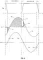
- Fig. 2 shows schematically time-course curves of the voltage U MP at the center tap of the frequency generator, the load circuit current I L2 and the gate voltage U gate of the lower (n-channel) MOS-FETs TU.
- the potential of the center tap MP is alternately at the positive potential of the supply voltage or at zero. Certain transition times t T occur during the trapezoidal capacitors CT connected in parallel with the two MOS-FETs, in which none of the switches TO and TU is conductive.
- transition times t T are intended, on the one hand, to improve the electromagnetic compatibility and, on the other hand, to minimize the switching losses: a drain-source voltage that rises too quickly would overlap too strongly with the drain current that did not drop as quickly as Cross over "), which can result in a high switch-off power loss.
- Both functions of the trapezoidal capacitors which can also be replaced by other circuit variants that act in an analog manner, are very important in the increased operating frequencies of the circuit according to the invention.
- the conduction state of a MOS-FET which contains an inherent body diode, consists on the one hand of the period of time to be seen in the lowest curve, in which the gate voltage lies below the threshold voltage U THR of the MOS-FET, and on the other hand from the time in which the Gate voltage is above the threshold voltage U THR and the transistor becomes conductive.
- the load circuit current I L2 flows monotonically increasing in both time ranges (with a time constant given by the load circuit impedances). Due to the resonant filter effect of the arrangement, however, there is such a strong relative damping of the harmonics contained therein that essentially the current sine wave shown in FIG. 2 predominates.
- the MOS-FET transistor Since the MOS-FET transistor is actually a bipolar switch, the current can flow through the transistor in both directions: through the conductive channel in one direction and through the body diode in the inverse direction.
- the current flow through the MOS-FETs therefore sets before the time period just described, ie before the threshold voltage U thr is reached by the opposite current flow through the so-called.
- the actual transistor current with a conductive channel is with I TU or I TO . The transition of the current from the diode to the channel takes place without loss since the voltage at the transistor is practically zero.
- the channel of the transistors is conductive, ie the threshold voltage U thr is reached before the load current I L2 changes its sign, ie while the load current flows into the body diode.
- the circuit is with a good design for outside temperatures from -35 ° C to +50 ° C and component temperatures between -35 ° C and + 125 ° C suitable, can be used with rectified supply voltages between 50 and 450 V are operated and designed for powers between 20 and 1000 W. will.
- the working frequencies can be between 100 kHz and 3 MHz lie. The values given correspond to the preliminary experimental Results and are not to be understood in any way restrictive. For supply voltages Class E circuitry may be below 50 V. be beneficial.
- the inductance is as high as possible the lamp coil L1, specifically to reduce the magnetizing current.
- This requires a ferrite material with high permeability and low Variations in both initial and amplitude permeability be used and with a minimal air gap and high permeance factor be applied. (It is primarily the temperature dependencies the permeability described in the introduction Angular frequency disturbances.)
- the reduction in the magnetizing current of the ferrite coupler L1 has a very advantageous effect on the phase angle ⁇ between the coupler voltage U 1 and the coupler current I 1 , as shown in FIG. 1.
- the current I 1 can be reduced for a specific power P 1 if ⁇ is 10 to 20 ° and consequently cos ⁇ is above 0.95, instead of 60 ° to 70 ° as with induction lamps with an open magnetic circuit, where cos ⁇ is below 0.5.
- the smaller current I 1 causes a smaller load current I L2 ; resulting smaller currents in the entire power generator result in smaller losses and a higher efficiency of the entire system.
- the HF generator can have a very high efficiency, well over 95%.
- the magnetic material of the coupler should be selected so that no specific losses of over 60 mW / cm 3 occur in the desired frequency range at the core temperatures to be expected (approximately 100-120 ° C.).
- a closed magnetic circuit with high inductance but low leakage inductance benefits radio interference suppression and the reduction in apparent system power.
Landscapes
- Circuit Arrangements For Discharge Lamps (AREA)
Applications Claiming Priority (2)
| Application Number | Priority Date | Filing Date | Title |
|---|---|---|---|
| DE19650110 | 1996-12-03 | ||
| DE19650110A DE19650110A1 (de) | 1996-12-03 | 1996-12-03 | Betriebsschaltung für eine elektrodenlose Niederdruckentladungslampe |
Publications (3)
| Publication Number | Publication Date |
|---|---|
| EP0852454A2 true EP0852454A2 (fr) | 1998-07-08 |
| EP0852454A3 EP0852454A3 (fr) | 1999-06-30 |
| EP0852454B1 EP0852454B1 (fr) | 2004-02-11 |
Family
ID=7813502
Family Applications (1)
| Application Number | Title | Priority Date | Filing Date |
|---|---|---|---|
| EP97120781A Expired - Lifetime EP0852454B1 (fr) | 1996-12-03 | 1997-11-26 | Circuit pour alimenter une lampe à décharge basse pression sans électrodes |
Country Status (10)
| Country | Link |
|---|---|
| US (1) | US5962987A (fr) |
| EP (1) | EP0852454B1 (fr) |
| JP (1) | JP4261628B2 (fr) |
| KR (1) | KR100443300B1 (fr) |
| CN (1) | CN1153508C (fr) |
| AT (1) | ATE259575T1 (fr) |
| AU (1) | AU733081B2 (fr) |
| CA (1) | CA2223085C (fr) |
| DE (2) | DE19650110A1 (fr) |
| HU (1) | HU220524B1 (fr) |
Families Citing this family (33)
| Publication number | Priority date | Publication date | Assignee | Title |
|---|---|---|---|---|
| US6313587B1 (en) * | 1998-01-13 | 2001-11-06 | Fusion Lighting, Inc. | High frequency inductive lamp and power oscillator |
| DE19805314A1 (de) | 1998-02-10 | 1999-08-19 | Patent Treuhand Ges Fuer Elektrische Gluehlampen Mbh | Schaltungsanordnung zum Betrieb mindestens einer elektrodenlosen Entladungslampe |
| TW439395B (en) * | 1998-10-06 | 2001-06-07 | Koninkl Philips Electronics Nv | Circuit arrangement |
| GB9923408D0 (en) * | 1999-10-05 | 1999-12-08 | Central Research Lab Ltd | A high frequency power oscillator |
| GB9923405D0 (en) * | 1999-10-05 | 1999-12-08 | Central Research Lab Ltd | A high frquency power oscillator |
| DE60143805D1 (de) * | 2000-10-31 | 2011-02-17 | Osram Sylvania Inc | Ballast-selbstoszillationswechselrichter mit phasengeregelter spannungsrückkopplung |
| DE10160790A1 (de) * | 2001-01-12 | 2002-08-08 | Patent Treuhand Ges Fuer Elektrische Gluehlampen Mbh | Schaltungsanordnung zum Einschalten einer Teilschaltungsanordnung |
| US7064494B2 (en) | 2001-04-12 | 2006-06-20 | Matsushita Electric Industrial Co., Ltd. | Discharge lamp operating apparatus and self-ballasted electrodeless discharge lamp |
| CA2349970A1 (fr) * | 2001-05-31 | 2002-11-30 | Martin Gagnon | Methode et dispositif de ventilation |
| DE10137305A1 (de) * | 2001-08-01 | 2003-02-13 | Patent Treuhand Ges Fuer Elektrische Gluehlampen Mbh | Freischwingende Schaltungsanordnung |
| US6727661B2 (en) | 2001-09-10 | 2004-04-27 | Matsushita Electric Industrial Co., Ltd. | Self-ballasted fluorescent lamp |
| GB2393336B (en) * | 2002-09-20 | 2005-07-20 | Coutant Lambda Ltd | Multi-resonant power conversion apparatus and methods |
| KR20060016072A (ko) * | 2002-12-31 | 2006-02-21 | 아포지 테크놀로지, 인크. | 적응적 공진 스위칭 전원 시스템 |
| US6906473B2 (en) * | 2003-08-26 | 2005-06-14 | Osram Sylvania Inc. | Feedback circuit and method of operating ballast resonant inverter |
| CN100534253C (zh) * | 2003-09-29 | 2009-08-26 | 光宝科技股份有限公司 | 快速温热点灯装置 |
| JP4186801B2 (ja) * | 2003-11-25 | 2008-11-26 | 松下電工株式会社 | 無電極放電灯点灯装置並びに無電極放電灯装置 |
| US7982405B2 (en) | 2005-03-22 | 2011-07-19 | Lightech Electronic Industries Ltd. | Igniter circuit for an HID lamp |
| TWI285519B (en) * | 2005-11-04 | 2007-08-11 | Delta Electronics Inc | Method adopting square voltage waveform for driving flat lamps |
| US7353771B2 (en) * | 2005-11-07 | 2008-04-08 | Mks Instruments, Inc. | Method and apparatus of providing power to ignite and sustain a plasma in a reactive gas generator |
| TW200721907A (en) * | 2005-11-18 | 2007-06-01 | Delta Optoelectronics Inc | An improved startup method for the mercury-free flat-fluorescent lamp |
| TW200740300A (en) * | 2006-04-04 | 2007-10-16 | Delta Optoelectronics Inc | Driving circuit and method for fluorescent lamp |
| TW200803141A (en) * | 2006-06-19 | 2008-01-01 | Hipro Electronic Co Ltd | Half-bridge resonant converter |
| US8138682B2 (en) * | 2007-05-10 | 2012-03-20 | Osram Sylvania Inc. | Symmetrical RF power supply for inductively coupled electrodeless lamps |
| FR2939006B1 (fr) * | 2008-11-26 | 2010-11-12 | Saint Gobain | Ballast pulse pour lampes planes |
| CN101489343B (zh) * | 2009-01-08 | 2012-07-04 | 王家诚 | 多段电感组合式电源emi滤波器 |
| US8692466B2 (en) | 2009-02-27 | 2014-04-08 | Mks Instruments Inc. | Method and apparatus of providing power to ignite and sustain a plasma in a reactive gas generator |
| US9134348B2 (en) | 2009-04-16 | 2015-09-15 | Panoramic Power Ltd. | Distributed electricity metering system |
| US9678114B2 (en) | 2009-04-16 | 2017-06-13 | Panoramic Power Ltd. | Apparatus and methods thereof for error correction in split core current transformers |
| CN102460188B (zh) | 2009-04-16 | 2015-09-16 | 全景电力有限公司 | 用于在断路器点的功率消耗测量的设备和方法 |
| US8797009B2 (en) * | 2010-07-06 | 2014-08-05 | Csr Technology Inc. | Auto cascode buck voltage converter |
| US9279722B2 (en) | 2012-04-30 | 2016-03-08 | Agilent Technologies, Inc. | Optical emission system including dichroic beam combiner |
| US9891252B2 (en) | 2015-07-28 | 2018-02-13 | Panoramic Power Ltd. | Thermal management of self-powered power sensors |
| US10024885B2 (en) | 2015-07-28 | 2018-07-17 | Panoramic Power Ltd. | Thermal management of self-powered power sensors |
Family Cites Families (17)
| Publication number | Priority date | Publication date | Assignee | Title |
|---|---|---|---|---|
| EP0442572B1 (fr) * | 1990-02-14 | 1995-05-03 | Koninklijke Philips Electronics N.V. | Dispositif de commutation |
| US5075600A (en) * | 1990-06-07 | 1991-12-24 | General Electric Company | Piezoelectrically actuated variable capacitor |
| US5138236B1 (en) * | 1991-05-28 | 1996-11-26 | Motorola Lighting Inc | Circuit for driving a gas discharge lamp load |
| US5306986A (en) * | 1992-05-20 | 1994-04-26 | Diablo Research Corporation | Zero-voltage complementary switching high efficiency class D amplifier |
| US5414327A (en) * | 1992-07-20 | 1995-05-09 | U.S. Philips Corporation | High frequency discharge lamp operating circuit with frequency control of the ignition voltage |
| US5382882A (en) * | 1993-04-20 | 1995-01-17 | General Electric Company | Power supply circuit for a gas discharge lamp |
| JP3419034B2 (ja) * | 1993-07-30 | 2003-06-23 | 東芝ライテック株式会社 | 無電極放電ランプ点灯装置 |
| GB2284077B (en) * | 1993-11-12 | 1998-03-04 | Johan Christiaan Fitter | A power converter |
| US5446350A (en) * | 1994-04-18 | 1995-08-29 | General Electric Company | Impedance matching circuit for an electrodeless fluorescent lamp ballast |
| US5406177A (en) * | 1994-04-18 | 1995-04-11 | General Electric Company | Gas discharge lamp ballast circuit with compact starting circuit |
| ATE177962T1 (de) * | 1994-07-22 | 1999-04-15 | Ruhrgas Ag | Vorrichtung zum automatischen schliessen einer absperrarmatur |
| US5691606A (en) * | 1994-09-30 | 1997-11-25 | Pacific Scientific Company | Ballast circuit for fluorescent lamp |
| DE4437453A1 (de) * | 1994-10-19 | 1996-04-25 | Patent Treuhand Ges Fuer Elektrische Gluehlampen Mbh | Verfahren zum Betrieb einer Entladungslampe und Schaltungsanordnung zum Betrieb einer Entladungslampe |
| GB2305311A (en) * | 1995-09-18 | 1997-04-02 | Gen Electric | Self oscillating drive circuit for an electrodeless discharge lamp |
| JPH09237687A (ja) * | 1995-12-26 | 1997-09-09 | Toshiba Lighting & Technol Corp | 無電極放電灯、無電極放電灯装置および照明装置 |
| JPH11514146A (ja) * | 1996-08-14 | 1999-11-30 | コーニンクレッカ、フィリップス、エレクトロニクス、エヌ.ヴィ. | 回路装置 |
| US5761056A (en) * | 1997-02-20 | 1998-06-02 | Boam R & D Co., Ltd. | Circuit for protecting fluorescent lamp from overload |
-
1996
- 1996-12-03 DE DE19650110A patent/DE19650110A1/de not_active Withdrawn
-
1997
- 1997-11-21 US US08/975,623 patent/US5962987A/en not_active Expired - Lifetime
- 1997-11-26 EP EP97120781A patent/EP0852454B1/fr not_active Expired - Lifetime
- 1997-11-26 DE DE59711298T patent/DE59711298D1/de not_active Expired - Lifetime
- 1997-11-26 AT AT97120781T patent/ATE259575T1/de not_active IP Right Cessation
- 1997-11-28 JP JP34446497A patent/JP4261628B2/ja not_active Expired - Fee Related
- 1997-12-01 CA CA002223085A patent/CA2223085C/fr not_active Expired - Fee Related
- 1997-12-02 HU HU9702329A patent/HU220524B1/hu not_active IP Right Cessation
- 1997-12-02 AU AU46839/97A patent/AU733081B2/en not_active Ceased
- 1997-12-03 KR KR1019970065499A patent/KR100443300B1/ko not_active Expired - Fee Related
- 1997-12-03 CN CNB971230803A patent/CN1153508C/zh not_active Expired - Fee Related
Also Published As
| Publication number | Publication date |
|---|---|
| CN1153508C (zh) | 2004-06-09 |
| DE19650110A1 (de) | 1998-06-04 |
| JPH10172776A (ja) | 1998-06-26 |
| HU9702329D0 (en) | 1998-03-02 |
| CA2223085C (fr) | 2005-04-05 |
| KR19980063729A (ko) | 1998-10-07 |
| DE59711298D1 (de) | 2004-03-18 |
| HU220524B1 (hu) | 2002-03-28 |
| EP0852454A3 (fr) | 1999-06-30 |
| AU733081B2 (en) | 2001-05-03 |
| EP0852454B1 (fr) | 2004-02-11 |
| CA2223085A1 (fr) | 1998-06-03 |
| KR100443300B1 (ko) | 2004-10-14 |
| HUP9702329A3 (en) | 2000-06-28 |
| HUP9702329A2 (hu) | 1998-08-28 |
| JP4261628B2 (ja) | 2009-04-30 |
| CN1184401A (zh) | 1998-06-10 |
| AU4683997A (en) | 1998-06-04 |
| US5962987A (en) | 1999-10-05 |
| ATE259575T1 (de) | 2004-02-15 |
Similar Documents
| Publication | Publication Date | Title |
|---|---|---|
| EP0852454B1 (fr) | Circuit pour alimenter une lampe à décharge basse pression sans électrodes | |
| DE69213632T2 (de) | Elektronisches Verschaltgerät für eine Kompaktleuchtstofflampe | |
| DE3789691T2 (de) | Schwingende Gleichrichterschaltung. | |
| DE3527622C2 (fr) | ||
| EP0781077A2 (fr) | Circuit pour alimenter une lampe | |
| DE69214769T2 (de) | Hochfrequenzenergieversorgungsvorrichtung für eine Leuchtstoffröhre mit Neonblasen- und Quecksilberwanderungsunterdrückung | |
| DE3306605A1 (de) | Stromversorgungsvorrichtung fuer zwei entladungslampen | |
| EP0681759B1 (fr) | Onduleur resonnant | |
| DE60011416T2 (de) | Einen wechselrichter einschliessende leistungsversorgungseinheit | |
| DE102017110927A1 (de) | Sperrwandlersteuerung, Sperrwandler und Verfahren zum Betreiben des Sperrwandlers | |
| DE69315761T2 (de) | Geschützter Umrichter zur Steuerung einer Entladungslampe | |
| DE10124219A1 (de) | Mikrowellenofen und Verfahren zum Steuern desselben | |
| DE69029301T2 (de) | Anzündanordnung für eine entladungslampe | |
| DE19729768B4 (de) | Schaltungsanordnung zum Zünden und Betreiben einer Leuchtstofflampe | |
| EP3667917A1 (fr) | Circuit de commande pour un circuit oscillateur destiné au fonctionnement des oscillateurs à alimentation parallèle | |
| DE4431050B4 (de) | Gleichspannungswandler | |
| DE19751063A1 (de) | Freischwingende Oszillatorschaltung mit einfacher Anlaufschaltung | |
| DE10118040A1 (de) | DC-DC Konverter | |
| EP0963032A1 (fr) | Convertisseur de courant alternatif en courant continu | |
| DE2624123A1 (de) | Speiseschaltung fuer niederdruck- entladungslampen | |
| EP1443808B1 (fr) | Circuit et méthode d'allumage et de commande du fonctionnement des lampes à décharge de gaz avec filaments de préchauffage | |
| EP1176851B1 (fr) | Dispositif pour lampe à décharge comportant un système de commutation pour le chauffage des électrodes | |
| DE69714163T2 (de) | Schaltungsanordnung | |
| EP1573891B1 (fr) | Convertisseur a resonance et procede pour alimenter des charges variables | |
| DE102009021048A1 (de) | Schaltung zum Beheizen wenigstens einer Heizwendel einer Gasentladungslampe, und Beleuchtungssystem |
Legal Events
| Date | Code | Title | Description |
|---|---|---|---|
| PUAI | Public reference made under article 153(3) epc to a published international application that has entered the european phase |
Free format text: ORIGINAL CODE: 0009012 |
|
| AK | Designated contracting states |
Kind code of ref document: A2 Designated state(s): AT BE CH DE ES FR GB IT LI NL SE |
|
| AX | Request for extension of the european patent |
Free format text: AL;LT;LV;MK;RO;SI |
|
| PUAL | Search report despatched |
Free format text: ORIGINAL CODE: 0009013 |
|
| AK | Designated contracting states |
Kind code of ref document: A3 Designated state(s): AT BE CH DE DK ES FI FR GB GR IE IT LI LU MC NL PT SE |
|
| AX | Request for extension of the european patent |
Free format text: AL;LT;LV;MK;RO;SI |
|
| RIC1 | Information provided on ipc code assigned before grant |
Free format text: 6H 05B 41/24 A, 6H 05B 41/29 B, 6H 05B 41/28 B |
|
| 17P | Request for examination filed |
Effective date: 19990720 |
|
| AKX | Designation fees paid |
Free format text: AT BE CH DE ES FR GB IT LI NL SE |
|
| 17Q | First examination report despatched |
Effective date: 20010831 |
|
| GRAH | Despatch of communication of intention to grant a patent |
Free format text: ORIGINAL CODE: EPIDOS IGRA |
|
| RIC1 | Information provided on ipc code assigned before grant |
Ipc: 7H 05B 41/28 A |
|
| GRAS | Grant fee paid |
Free format text: ORIGINAL CODE: EPIDOSNIGR3 |
|
| GRAA | (expected) grant |
Free format text: ORIGINAL CODE: 0009210 |
|
| AK | Designated contracting states |
Kind code of ref document: B1 Designated state(s): AT BE CH DE ES FR GB IT LI NL SE |
|
| REG | Reference to a national code |
Ref country code: GB Ref legal event code: FG4D Free format text: NOT ENGLISH |
|
| REG | Reference to a national code |
Ref country code: CH Ref legal event code: EP |
|
| REF | Corresponds to: |
Ref document number: 59711298 Country of ref document: DE Date of ref document: 20040318 Kind code of ref document: P |
|
| PG25 | Lapsed in a contracting state [announced via postgrant information from national office to epo] |
Ref country code: SE Free format text: LAPSE BECAUSE OF FAILURE TO SUBMIT A TRANSLATION OF THE DESCRIPTION OR TO PAY THE FEE WITHIN THE PRESCRIBED TIME-LIMIT Effective date: 20040511 |
|
| GBT | Gb: translation of ep patent filed (gb section 77(6)(a)/1977) |
Effective date: 20040416 |
|
| PG25 | Lapsed in a contracting state [announced via postgrant information from national office to epo] |
Ref country code: ES Free format text: LAPSE BECAUSE OF FAILURE TO SUBMIT A TRANSLATION OF THE DESCRIPTION OR TO PAY THE FEE WITHIN THE PRESCRIBED TIME-LIMIT Effective date: 20040522 |
|
| ET | Fr: translation filed | ||
| PG25 | Lapsed in a contracting state [announced via postgrant information from national office to epo] |
Ref country code: AT Free format text: LAPSE BECAUSE OF NON-PAYMENT OF DUE FEES Effective date: 20041126 |
|
| PG25 | Lapsed in a contracting state [announced via postgrant information from national office to epo] |
Ref country code: LI Free format text: LAPSE BECAUSE OF NON-PAYMENT OF DUE FEES Effective date: 20041130 Ref country code: CH Free format text: LAPSE BECAUSE OF NON-PAYMENT OF DUE FEES Effective date: 20041130 |
|
| PLBE | No opposition filed within time limit |
Free format text: ORIGINAL CODE: 0009261 |
|
| STAA | Information on the status of an ep patent application or granted ep patent |
Free format text: STATUS: NO OPPOSITION FILED WITHIN TIME LIMIT |
|
| 26N | No opposition filed |
Effective date: 20041112 |
|
| REG | Reference to a national code |
Ref country code: CH Ref legal event code: PL |
|
| PGFP | Annual fee paid to national office [announced via postgrant information from national office to epo] |
Ref country code: NL Payment date: 20051109 Year of fee payment: 9 |
|
| PGFP | Annual fee paid to national office [announced via postgrant information from national office to epo] |
Ref country code: FR Payment date: 20051122 Year of fee payment: 9 |
|
| PGFP | Annual fee paid to national office [announced via postgrant information from national office to epo] |
Ref country code: IT Payment date: 20061130 Year of fee payment: 10 |
|
| PG25 | Lapsed in a contracting state [announced via postgrant information from national office to epo] |
Ref country code: NL Free format text: LAPSE BECAUSE OF NON-PAYMENT OF DUE FEES Effective date: 20070601 |
|
| NLV4 | Nl: lapsed or anulled due to non-payment of the annual fee |
Effective date: 20070601 |
|
| REG | Reference to a national code |
Ref country code: FR Ref legal event code: ST Effective date: 20070731 |
|
| PG25 | Lapsed in a contracting state [announced via postgrant information from national office to epo] |
Ref country code: FR Free format text: LAPSE BECAUSE OF NON-PAYMENT OF DUE FEES Effective date: 20061130 |
|
| PG25 | Lapsed in a contracting state [announced via postgrant information from national office to epo] |
Ref country code: IT Free format text: LAPSE BECAUSE OF NON-PAYMENT OF DUE FEES Effective date: 20071126 |
|
| REG | Reference to a national code |
Ref country code: DE Ref legal event code: R081 Ref document number: 59711298 Country of ref document: DE Owner name: OSRAM GMBH, DE Free format text: FORMER OWNER: OSRAM GESELLSCHAFT MIT BESCHRAENKTER HAFTUNG, 81543 MUENCHEN, DE Effective date: 20111130 |
|
| REG | Reference to a national code |
Ref country code: DE Ref legal event code: R081 Ref document number: 59711298 Country of ref document: DE Owner name: OSRAM GMBH, DE Free format text: FORMER OWNER: OSRAM AG, 81543 MUENCHEN, DE Effective date: 20130205 |
|
| REG | Reference to a national code |
Ref country code: DE Ref legal event code: R081 Ref document number: 59711298 Country of ref document: DE Owner name: OSRAM GMBH, DE Free format text: FORMER OWNER: OSRAM GMBH, 81543 MUENCHEN, DE Effective date: 20130822 |
|
| PGFP | Annual fee paid to national office [announced via postgrant information from national office to epo] |
Ref country code: GB Payment date: 20141119 Year of fee payment: 18 Ref country code: DE Payment date: 20141119 Year of fee payment: 18 |
|
| PGFP | Annual fee paid to national office [announced via postgrant information from national office to epo] |
Ref country code: BE Payment date: 20141118 Year of fee payment: 18 |
|
| REG | Reference to a national code |
Ref country code: DE Ref legal event code: R119 Ref document number: 59711298 Country of ref document: DE |
|
| GBPC | Gb: european patent ceased through non-payment of renewal fee |
Effective date: 20151126 |
|
| PG25 | Lapsed in a contracting state [announced via postgrant information from national office to epo] |
Ref country code: DE Free format text: LAPSE BECAUSE OF NON-PAYMENT OF DUE FEES Effective date: 20160601 Ref country code: GB Free format text: LAPSE BECAUSE OF NON-PAYMENT OF DUE FEES Effective date: 20151126 |
|
| PG25 | Lapsed in a contracting state [announced via postgrant information from national office to epo] |
Ref country code: BE Free format text: LAPSE BECAUSE OF NON-PAYMENT OF DUE FEES Effective date: 20151130 |