EP0855745A2 - Verfahren zur Herstellung einer Farbfiltermatrix - Google Patents
Verfahren zur Herstellung einer Farbfiltermatrix Download PDFInfo
- Publication number
- EP0855745A2 EP0855745A2 EP98200058A EP98200058A EP0855745A2 EP 0855745 A2 EP0855745 A2 EP 0855745A2 EP 98200058 A EP98200058 A EP 98200058A EP 98200058 A EP98200058 A EP 98200058A EP 0855745 A2 EP0855745 A2 EP 0855745A2
- Authority
- EP
- European Patent Office
- Prior art keywords
- substrate
- colorant
- layer
- heat transferable
- layers
- Prior art date
- Legal status (The legal status is an assumption and is not a legal conclusion. Google has not performed a legal analysis and makes no representation as to the accuracy of the status listed.)
- Withdrawn
Links
- 238000004519 manufacturing process Methods 0.000 title claims abstract description 12
- 238000003491 array Methods 0.000 title description 16
- 239000000758 substrate Substances 0.000 claims abstract description 179
- 239000003086 colorant Substances 0.000 claims abstract description 165
- 239000000463 material Substances 0.000 claims abstract description 47
- 238000000034 method Methods 0.000 claims abstract description 46
- 238000012546 transfer Methods 0.000 claims abstract description 24
- 238000010438 heat treatment Methods 0.000 claims abstract description 14
- 239000000126 substance Substances 0.000 claims abstract description 12
- 238000005530 etching Methods 0.000 claims abstract description 9
- 238000005498 polishing Methods 0.000 claims abstract description 7
- 229920002120 photoresistant polymer Polymers 0.000 claims description 86
- 230000001737 promoting effect Effects 0.000 claims description 18
- 238000000151 deposition Methods 0.000 claims description 14
- 238000000059 patterning Methods 0.000 claims description 12
- 239000010410 layer Substances 0.000 description 170
- 239000000049 pigment Substances 0.000 description 35
- 239000011888 foil Substances 0.000 description 18
- XUIMIQQOPSSXEZ-UHFFFAOYSA-N Silicon Chemical compound [Si] XUIMIQQOPSSXEZ-UHFFFAOYSA-N 0.000 description 14
- 229910052710 silicon Inorganic materials 0.000 description 14
- 239000010703 silicon Substances 0.000 description 14
- 238000000576 coating method Methods 0.000 description 12
- 239000011248 coating agent Substances 0.000 description 10
- 239000011521 glass Substances 0.000 description 10
- 239000000975 dye Substances 0.000 description 8
- IEQIEDJGQAUEQZ-UHFFFAOYSA-N phthalocyanine Chemical compound N1C(N=C2C3=CC=CC=C3C(N=C3C4=CC=CC=C4C(=N4)N3)=N2)=C(C=CC=C2)C2=C1N=C1C2=CC=CC=C2C4=N1 IEQIEDJGQAUEQZ-UHFFFAOYSA-N 0.000 description 8
- 238000005240 physical vapour deposition Methods 0.000 description 8
- 229910001220 stainless steel Inorganic materials 0.000 description 7
- 239000010935 stainless steel Substances 0.000 description 7
- -1 Pigment Yellow 151 Chemical class 0.000 description 6
- 229910052715 tantalum Inorganic materials 0.000 description 5
- GUVRBAGPIYLISA-UHFFFAOYSA-N tantalum atom Chemical compound [Ta] GUVRBAGPIYLISA-UHFFFAOYSA-N 0.000 description 5
- CSCPPACGZOOCGX-UHFFFAOYSA-N Acetone Chemical compound CC(C)=O CSCPPACGZOOCGX-UHFFFAOYSA-N 0.000 description 4
- 229910000831 Steel Inorganic materials 0.000 description 4
- 239000002131 composite material Substances 0.000 description 4
- 239000002019 doping agent Substances 0.000 description 4
- 239000010959 steel Substances 0.000 description 4
- 229920013683 Celanese Polymers 0.000 description 3
- VYPSYNLAJGMNEJ-UHFFFAOYSA-N Silicium dioxide Chemical compound O=[Si]=O VYPSYNLAJGMNEJ-UHFFFAOYSA-N 0.000 description 3
- 238000011109 contamination Methods 0.000 description 3
- 238000011161 development Methods 0.000 description 3
- 230000005670 electromagnetic radiation Effects 0.000 description 3
- RBTKNAXYKSUFRK-UHFFFAOYSA-N heliogen blue Chemical compound [Cu].[N-]1C2=C(C=CC=C3)C3=C1N=C([N-]1)C3=CC=CC=C3C1=NC([N-]1)=C(C=CC=C3)C3=C1N=C([N-]1)C3=CC=CC=C3C1=N2 RBTKNAXYKSUFRK-UHFFFAOYSA-N 0.000 description 3
- 229910052751 metal Inorganic materials 0.000 description 3
- 239000002184 metal Substances 0.000 description 3
- SJHHDDDGXWOYOE-UHFFFAOYSA-N oxytitamium phthalocyanine Chemical compound [Ti+2]=O.C12=CC=CC=C2C(N=C2[N-]C(C3=CC=CC=C32)=N2)=NC1=NC([C]1C=CC=CC1=1)=NC=1N=C1[C]3C=CC=CC3=C2[N-]1 SJHHDDDGXWOYOE-UHFFFAOYSA-N 0.000 description 3
- 238000002202 sandwich sublimation Methods 0.000 description 3
- 235000019239 indanthrene blue RS Nutrition 0.000 description 2
- 239000004973 liquid crystal related substance Substances 0.000 description 2
- 238000004377 microelectronic Methods 0.000 description 2
- 230000003287 optical effect Effects 0.000 description 2
- 238000007517 polishing process Methods 0.000 description 2
- 229920000642 polymer Polymers 0.000 description 2
- 239000002356 single layer Substances 0.000 description 2
- WGTYBPLFGIVFAS-UHFFFAOYSA-M tetramethylammonium hydroxide Chemical compound [OH-].C[N+](C)(C)C WGTYBPLFGIVFAS-UHFFFAOYSA-M 0.000 description 2
- CYAWSKDLLFELCJ-UHFFFAOYSA-N 6H-imidazo[4,5-e]benzimidazol-2-one Chemical class N=1C(N=C2C=CC3=C(N=CN3)C21)=O CYAWSKDLLFELCJ-UHFFFAOYSA-N 0.000 description 1
- RKFMOTBTFHXWCM-UHFFFAOYSA-M [AlH2]O Chemical compound [AlH2]O RKFMOTBTFHXWCM-UHFFFAOYSA-M 0.000 description 1
- LBGCRGLFTKVXDZ-UHFFFAOYSA-M ac1mc2aw Chemical compound [Al+3].[Cl-].C12=CC=CC=C2C(N=C2[N-]C(C3=CC=CC=C32)=N2)=NC1=NC([C]1C=CC=CC1=1)=NC=1N=C1[C]3C=CC=CC3=C2[N-]1 LBGCRGLFTKVXDZ-UHFFFAOYSA-M 0.000 description 1
- 229910052782 aluminium Inorganic materials 0.000 description 1
- XAGFODPZIPBFFR-UHFFFAOYSA-N aluminium Chemical compound [Al] XAGFODPZIPBFFR-UHFFFAOYSA-N 0.000 description 1
- 150000008641 benzimidazolones Chemical class 0.000 description 1
- WDEQGLDWZMIMJM-UHFFFAOYSA-N benzyl 4-hydroxy-2-(hydroxymethyl)pyrrolidine-1-carboxylate Chemical compound OCC1CC(O)CN1C(=O)OCC1=CC=CC=C1 WDEQGLDWZMIMJM-UHFFFAOYSA-N 0.000 description 1
- 230000015572 biosynthetic process Effects 0.000 description 1
- 238000005229 chemical vapour deposition Methods 0.000 description 1
- 238000010276 construction Methods 0.000 description 1
- XCJYREBRNVKWGJ-UHFFFAOYSA-N copper(II) phthalocyanine Chemical compound [Cu+2].C12=CC=CC=C2C(N=C2[N-]C(C3=CC=CC=C32)=N2)=NC1=NC([C]1C=CC=CC1=1)=NC=1N=C1[C]3C=CC=CC3=C2[N-]1 XCJYREBRNVKWGJ-UHFFFAOYSA-N 0.000 description 1
- 239000013078 crystal Substances 0.000 description 1
- 230000008021 deposition Effects 0.000 description 1
- 238000005137 deposition process Methods 0.000 description 1
- 150000005125 dioxazines Chemical class 0.000 description 1
- VPWFPZBFBFHIIL-UHFFFAOYSA-L disodium 4-[(4-methyl-2-sulfophenyl)diazenyl]-3-oxidonaphthalene-2-carboxylate Chemical compound [Na+].[Na+].[O-]S(=O)(=O)C1=CC(C)=CC=C1N=NC1=C(O)C(C([O-])=O)=CC2=CC=CC=C12 VPWFPZBFBFHIIL-UHFFFAOYSA-L 0.000 description 1
- 238000005562 fading Methods 0.000 description 1
- 239000012530 fluid Substances 0.000 description 1
- 238000003384 imaging method Methods 0.000 description 1
- PXZQEOJJUGGUIB-UHFFFAOYSA-N isoindolin-1-one Chemical class C1=CC=C2C(=O)NCC2=C1 PXZQEOJJUGGUIB-UHFFFAOYSA-N 0.000 description 1
- GWVMLCQWXVFZCN-UHFFFAOYSA-N isoindoline Chemical class C1=CC=C2CNCC2=C1 GWVMLCQWXVFZCN-UHFFFAOYSA-N 0.000 description 1
- BSIHWSXXPBAGTC-UHFFFAOYSA-N isoviolanthrone Chemical compound C12=CC=CC=C2C(=O)C2=CC=C3C(C4=C56)=CC=C5C5=CC=CC=C5C(=O)C6=CC=C4C4=C3C2=C1C=C4 BSIHWSXXPBAGTC-UHFFFAOYSA-N 0.000 description 1
- 238000001459 lithography Methods 0.000 description 1
- 238000012423 maintenance Methods 0.000 description 1
- 150000002739 metals Chemical class 0.000 description 1
- 238000012544 monitoring process Methods 0.000 description 1
- 229920000620 organic polymer Polymers 0.000 description 1
- YRZZLAGRKZIJJI-UHFFFAOYSA-N oxyvanadium phthalocyanine Chemical compound [V+2]=O.C12=CC=CC=C2C(N=C2[N-]C(C3=CC=CC=C32)=N2)=NC1=NC([C]1C=CC=CC1=1)=NC=1N=C1[C]3C=CC=CC3=C2[N-]1 YRZZLAGRKZIJJI-UHFFFAOYSA-N 0.000 description 1
- 239000002245 particle Substances 0.000 description 1
- 239000011236 particulate material Substances 0.000 description 1
- 150000002979 perylenes Chemical class 0.000 description 1
- CLYVDMAATCIVBF-UHFFFAOYSA-N pigment red 224 Chemical compound C=12C3=CC=C(C(OC4=O)=O)C2=C4C=CC=1C1=CC=C2C(=O)OC(=O)C4=CC=C3C1=C42 CLYVDMAATCIVBF-UHFFFAOYSA-N 0.000 description 1
- 229940067265 pigment yellow 138 Drugs 0.000 description 1
- 239000004033 plastic Substances 0.000 description 1
- 229920001721 polyimide Polymers 0.000 description 1
- 238000002360 preparation method Methods 0.000 description 1
- 238000000746 purification Methods 0.000 description 1
- YRJYANBGTAMXRQ-UHFFFAOYSA-N pyrazolo[3,4-h]quinazolin-2-one Chemical class C1=C2N=NC=C2C2=NC(=O)N=CC2=C1 YRJYANBGTAMXRQ-UHFFFAOYSA-N 0.000 description 1
- 239000010453 quartz Substances 0.000 description 1
- 239000004065 semiconductor Substances 0.000 description 1
- 239000000377 silicon dioxide Substances 0.000 description 1
- 239000002904 solvent Substances 0.000 description 1
- 238000004528 spin coating Methods 0.000 description 1
- 239000000725 suspension Substances 0.000 description 1
- 238000002604 ultrasonography Methods 0.000 description 1
- 238000001771 vacuum deposition Methods 0.000 description 1
- 239000002699 waste material Substances 0.000 description 1
- XLYOFNOQVPJJNP-UHFFFAOYSA-N water Substances O XLYOFNOQVPJJNP-UHFFFAOYSA-N 0.000 description 1
Images


Classifications
-
- B—PERFORMING OPERATIONS; TRANSPORTING
- B41—PRINTING; LINING MACHINES; TYPEWRITERS; STAMPS
- B41M—PRINTING, DUPLICATING, MARKING, OR COPYING PROCESSES; COLOUR PRINTING
- B41M5/00—Duplicating or marking methods; Sheet materials for use therein
- B41M5/26—Thermography ; Marking by high energetic means, e.g. laser otherwise than by burning, and characterised by the material used
- B41M5/382—Contact thermal transfer or sublimation processes
- B41M5/38207—Contact thermal transfer or sublimation processes characterised by aspects not provided for in groups B41M5/385 - B41M5/395
-
- B—PERFORMING OPERATIONS; TRANSPORTING
- B41—PRINTING; LINING MACHINES; TYPEWRITERS; STAMPS
- B41M—PRINTING, DUPLICATING, MARKING, OR COPYING PROCESSES; COLOUR PRINTING
- B41M5/00—Duplicating or marking methods; Sheet materials for use therein
- B41M5/26—Thermography ; Marking by high energetic means, e.g. laser otherwise than by burning, and characterised by the material used
- B41M5/265—Thermography ; Marking by high energetic means, e.g. laser otherwise than by burning, and characterised by the material used for the production of optical filters or electrical components
-
- C—CHEMISTRY; METALLURGY
- C23—COATING METALLIC MATERIAL; COATING MATERIAL WITH METALLIC MATERIAL; CHEMICAL SURFACE TREATMENT; DIFFUSION TREATMENT OF METALLIC MATERIAL; COATING BY VACUUM EVAPORATION, BY SPUTTERING, BY ION IMPLANTATION OR BY CHEMICAL VAPOUR DEPOSITION, IN GENERAL; INHIBITING CORROSION OF METALLIC MATERIAL OR INCRUSTATION IN GENERAL
- C23C—COATING METALLIC MATERIAL; COATING MATERIAL WITH METALLIC MATERIAL; SURFACE TREATMENT OF METALLIC MATERIAL BY DIFFUSION INTO THE SURFACE, BY CHEMICAL CONVERSION OR SUBSTITUTION; COATING BY VACUUM EVAPORATION, BY SPUTTERING, BY ION IMPLANTATION OR BY CHEMICAL VAPOUR DEPOSITION, IN GENERAL
- C23C14/00—Coating by vacuum evaporation, by sputtering or by ion implantation of the coating forming material
- C23C14/06—Coating by vacuum evaporation, by sputtering or by ion implantation of the coating forming material characterised by the coating material
- C23C14/12—Organic material
-
- G—PHYSICS
- G02—OPTICS
- G02B—OPTICAL ELEMENTS, SYSTEMS OR APPARATUS
- G02B5/00—Optical elements other than lenses
- G02B5/20—Filters
- G02B5/201—Filters in the form of arrays
-
- G—PHYSICS
- G03—PHOTOGRAPHY; CINEMATOGRAPHY; ANALOGOUS TECHNIQUES USING WAVES OTHER THAN OPTICAL WAVES; ELECTROGRAPHY; HOLOGRAPHY
- G03F—PHOTOMECHANICAL PRODUCTION OF TEXTURED OR PATTERNED SURFACES, e.g. FOR PRINTING, FOR PROCESSING OF SEMICONDUCTOR DEVICES; MATERIALS THEREFOR; ORIGINALS THEREFOR; APPARATUS SPECIALLY ADAPTED THEREFOR
- G03F7/00—Photomechanical, e.g. photolithographic, production of textured or patterned surfaces, e.g. printing surfaces; Materials therefor, e.g. comprising photoresists; Apparatus specially adapted therefor
- G03F7/0005—Production of optical devices or components in so far as characterised by the lithographic processes or materials used therefor
- G03F7/0007—Filters, e.g. additive colour filters; Components for display devices
-
- B—PERFORMING OPERATIONS; TRANSPORTING
- B41—PRINTING; LINING MACHINES; TYPEWRITERS; STAMPS
- B41M—PRINTING, DUPLICATING, MARKING, OR COPYING PROCESSES; COLOUR PRINTING
- B41M5/00—Duplicating or marking methods; Sheet materials for use therein
- B41M5/26—Thermography ; Marking by high energetic means, e.g. laser otherwise than by burning, and characterised by the material used
- B41M5/382—Contact thermal transfer or sublimation processes
- B41M5/38207—Contact thermal transfer or sublimation processes characterised by aspects not provided for in groups B41M5/385 - B41M5/395
- B41M5/38214—Structural details, e.g. multilayer systems
-
- B—PERFORMING OPERATIONS; TRANSPORTING
- B41—PRINTING; LINING MACHINES; TYPEWRITERS; STAMPS
- B41M—PRINTING, DUPLICATING, MARKING, OR COPYING PROCESSES; COLOUR PRINTING
- B41M5/00—Duplicating or marking methods; Sheet materials for use therein
- B41M5/26—Thermography ; Marking by high energetic means, e.g. laser otherwise than by burning, and characterised by the material used
- B41M5/382—Contact thermal transfer or sublimation processes
- B41M5/385—Contact thermal transfer or sublimation processes characterised by the transferable dyes or pigments
Definitions
- the present invention is related to U.S. Patent Application Serial No. 08/648,772 filed May. 16, 1996 and entitled Method of Forming an Organic Electroluminescent Display Panel, by Littman, et al.
- the disclosure of this related application is incorporated herein by reference.
- the present invention relates to methods of making color filter arrays which are suitable for display applications such as liquid crystal displays or light emitting diode displays and are particularly suitable for use on image sensors.
- FIG. 1 shows a method for making coatings from evaporated organic colorants
- a substrate 102 is positioned adjacent to an aperture mask 104.
- the aperture mask provides an aperture over a portion of the substrate.
- An organic colorant which is to provide the coating is placed into a source boat 100, which is heated by passing an electric current through it. Alternatively, the boat may be heated by the application of radiant heating from a suitably placed heat source. Upon being heated under reduced pressure, the colorant vaporizes and travels from the source, impinging on mask 105. The portion of colorant vapor which passes through the opening in mask 105 travels along the lines 103, and between those lines, depositing on the substrate 102 and mask 104.
- PVD physical vapor deposition
- Some other problems in making color filter arrays by the PVD process are the need to use a large source-to-substrate spacing which requires large chambers and large pumps to reach a sufficient vacuum, and the need for masks which cause low-material utilization and build-up on the mask with the concomitant contamination problems. Very specific off-axis source location relative to the substrate, which is sometimes needed for uniform coating, causes very poor material utilization. Still further, source replenishment problems exist for coating multiple substrates in one pump-down. In addition, when multiple layers are deposited, the process needs to be carefully monitored for the thickness of layers in the multiple colorant coatings in multiple cycles.
- the present invention provides in one embodiment a method of making a color filter array on a first substrate comprising the steps of:
- the present invention provides a method of making a color filter array on a first substrate comprising the steps of:
- the present invention provides a method of making a color filter array on a first substrate comprising the steps of:
- Still another embodiment of the present invention provides a method of making a color filter array on a first substrate comprising the steps of:
- Advantages of this technique include the ability to form colorant layers with tuned colors by co-deposition of a plurality of colorant materials in a single step, along with the ability to pattern the colorant layers to form an array of colorant elements.
- it provides for an evaporative purification of the colorant during the preparation of the transferable colorant coating and the effective utilization of evaporant materials with high quality uniformity over a large areas.
- Other advantages include precise control of layer thickness, lower maintenance of deposition vacuum chambers, and minimal monitoring for the deposition process.
- Still further, it offers the ability to coat at higher pressures and in smaller vacuum chambers which permit faster cycle time and the use of lower-cost vacuum equipment than for standard PVD techniques.
- FIG. 1 shows a typical configuration for conventional physical vapor deposition (PVD).
- FIG. 2 shows a typical configuration for the thermal transfer of a material from an intermediate substrate to the final substrate, according to the present invention.
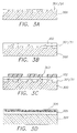
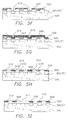
- FIGS. 3A-H show various steps in a method according to the present invention for making color filter arrays.
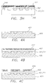
- FIGS. 4A-F show various steps in another method according to the present invention for making color filter arrays.
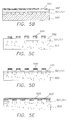
- FIGS. 5A-I show various steps in another method according to the present invention for making color filter arrays.
- FIGS. 6A-I show various steps in another method according to the present invention for making color filter arrays.
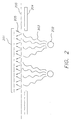
- FIG. 1 an arrangement for conventional PVD is shown, including a heated source 100, containing the material to be deposited, the substrate 102, and masks 104 and 105 which restrict the material vapor to paths 103 and the region in between.
- FIG. 2 is shown a configuration for the transfer of a material which has been deposited as a coating on the second substrate 200, onto the first substrate 201 as indicated by the arrows 205 and which is promoted by heating with heat source 202 as indicated by radiant heat 203 acting through an aperture 204.
- Color filter arrays may be fabricated using evaporated colorants which do not involve any receiving polymer.
- a typical process is as follows: A photoresist layer is coated on a transparent substrate such as glass which is to be incorporated as an optical element in a device, for example in a liquid crystal display, a light emitting diode display, an imaging sensor, or other such device. Thereafter, the substrate is patterned to form openings over the regions which are to pass filtered light or light which is to be filtered, depending on the relative orientation of the substrate and the light source. Colorant materials, generally pigments, are then deposited over the patterned photoresist layer to form a colorant layer in the openings over the substrate.
- the unwanted colorant is removed by chemical mechanical polishing, in which particles of an abrasive substance such as silica with mean diameters of less than 0.5 micrometers are suspended in a fluid medium such as aqueous tetramethylammonium hydroxide and the surface to be polished is moved in relation to a pad which is wetted with the suspension.
- a fluid medium such as aqueous tetramethylammonium hydroxide
- the colorant which is positioned over the selected regions is not removed due to its lower profile relative to the surface of the unwanted colorant.
- the unwanted colorant may be removed by lifting-off the patterned photoresist layer and the overlying colorant layer.
- Color filter arrays may also be fabricated in another process, using evaporated colorants which do not involve any receiving polymer.
- a typical process is as follows: A colorant or a plurality of colorants, generally pigments, is deposited on a substrate. Thereafter, a photoresist layer is coated on the colorant layer and then patterned to leave photoresist in place over selected regions of the substrate through which is to pass filtered light or light which is to be filtered. An etch process is now performed and the patterned photoresist layer acts as a mask for the colorant layer, such that the colorant is removed except over the selected regions.
- the substrate which may be a transparent substrate such as glass
- the regions 31 in a transparent substrate may actually extend to include the full thickness of the substrate, and are not limited to only a portion of that thickness.
- regions 31 can be processed beforehand to provide wells for different dopant materials to form pixels 301.
- the substrate may be a composite of different layers and in particular may include an adhesion promoting layer 302.
- an adhesion-promoting layer 302 is formed as part of the substrate 300 and above regions 31 (or in pixels 301 in a silicon based substrate).
- the adhesion-promoting layer 302 can be formed by a number of techniques including spin-coating of an organic polymer or a spin-on glass, or by chemical vapor deposition.
- the adhesion promoting layer may be patterned to form recesses in the adhesion promoting layer above the pixels.
- the adhesion-promoting layer 302 may be applied after formation of the patterned photoresist layer 303, discussed below in FIG. 3C.
- a spin-coated photoresist layer is patterned to provide openings over the selected regions 31 (which can be pixels 301).
- Such patterning techniques are well known to those skilled in the art.
- the photoresist layer can be imagewise exposed to light, illuminating particular areas of the layer.
- a development step is then used to form openings over the region 31 (pixels 301) providing the desired pattern.
- a layer 305 having a colorant is formed on the substrate 304, and another colorant layer 306 is formed on layer 305.
- the colorant layers are formed by physical vapor deposition, which provides uniform layers of controlled thickness, containing no materials with higher volatility than the colorants.
- the colorant layers 305 and 306 can be organic colorants which are transferable upon the application of energy such as heat.
- the colorant is vaporized by heating under reduced pressure, and condensed on a moving strip of stainless steel foil which is passed over the heated source at a constant rate.
- the substrate 304 and colorant layers 305 and 306 are shown positioned relative to the substrate 300 and the regions 31 (or pixels 301) in the substrate. In the process it is desired to transfer the colorant layers 305 and 306 onto the substrate and the pixels.
- the transferred colorant layers are depicted as a single layer now labeled number 307.
- heat is applied to the substrate 304.
- the substrate is composed of metals, such as steel or aluminum or of a temperature-resistant plastic such as a polyimide film. Heating is often done by exposing the non-coated side of the substrate 304 to electromagnetic radiation of wavelengths which are absorbed by the substrate (or by the colorant coating in the cases where the substrate is substantially transparent) and are converted into heat by radiationless decay processes.
- the electromagnetic radiation may be applied over a large area simultaneously as from an extended lamp source, or it may be applied as a scanned beam as with a laser.
- imagewise light exposure may be used to heat and transfer only a portion of the colorant coating.
- Another method used to heat substrate 304 in order to transfer the colorant layers 305 and 306 is to pass an electric current through the substrate, particularly when the substrate used is composed entirely or partially of metal.
- the substrate may be heated by direct contact with an object such as a metal block, a high temperature roller, or other such devices which can be heated or pre-heated to the required temperature and which can transfer heat to the substrate by direct thermal contact.
- Typical distances and pressures for the transfer of colorant are from about 0.1 mm to about 3 mm at pressures of less than or equal to about 0.1 Torr, up to a distance of about 50 mm at pressures of less than or equal to 0.001 Torr.
- FIG. 3G shows the color filter array after a lift-off process.
- the lift-off process is needed to remove unwanted portions of the photoresist layer 303 and the portions of the colorant layer 307 on the unwanted portions of the photoresist layer 303, leaving behind colorant layers 38 over the selected regions 39 (or pixels 309).
- the lift-off process is as follows:
- a photoresist layer is patterned by imagewise exposure to electromagnetic radiation of the appropriate wavelength followed by development to open up areas where a subsequently deposited layer is desired.
- the subsequent layer is deposited on both the opened areas and the remaining photoresist, followed by the lift-off, in which the photoresist is dissolved or swollen in a solvent, causing it to become detached from the underlying substrate, lifting-off to leave the desired deposit in place.
- a description of the lift-off process and typical materials used is given in chapter 12 of Semiconductor Lithography, by W.M. Moreau, Plenum Press, N.Y., 1989.
- a second embodiment for the preset invention is seen viewing FIG. 3H with respect to FIG. 3F.
- the color filter is seen after a chemical mechanical polishing process.
- the chemical mechanical polishing process is needed to remove unwanted portions of the photoresist layer 303 and portions of layer 307 (which can be one or more colorant layers) leaving behind colorant layers 310 of the selected regions 31 (or pixels 301) and photoresist layer 311 over the remaining areas.
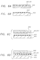
- the substrate (which can be either a silicon substrate or a transparent substrate such as glass) in which are depicted regions 41 through which filtered light will pass or light that is to be filtered (regions 41 can be pixels 401 which are to receive filtered light, in the case of a silicon substrate which has already been processed to provide wells for different dopant materials (to form pixels 401).
- the substrate may be a composite of different layers, and in particular may include an adhesion promoting layer.
- an adhesion promoting layer 402 which can be subsequently etched is formed as part of the substrate 400 with regions 41 (which can be pixels 401) and a layer of photoresist 403 is formed above it.
- the photoresist is exposed and developed to form openings over selected regions 41 (or pixels 401), leaving photoresist 404 over the rest of the layer 402.
- the openings in the patterned resist layer 404 are used as a mask for an etch of the substrate 400, to produce a pattern of recesses in the adhesion promoting layer, now numbered 405.
- the etch may be performed so as to etch through the adhesion promoting layer 405 into the rest of substrate 400.
- a colorant layer is deposited on the patterned resist layer 404 and the recesses in underlying layer 405 to give layer 406/407.
- the colorant 406 which is not above the selected regions 41 (which can be pixels 401 in the case of a silicon substrate) and the patterned photoresist layer 404 is removed by chemical mechanical polishing, to leave the patterned layer 405 and the colorant 407 above the selected regions 41 (or pixels, 401).
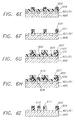
- FIG. 5A in which a substrate 500 (which can range from a transparent glass to a silicon based substrate) is shown having regions 51 through which filtered light will pass or light which is to be filtered.
- the substrate 500 is silicon
- the substrate can already have been processed to provide wells for different dopant materials to form pixels 501 which are to receive filtered light.
- the substrate may be a composite of different layers, and in particular may include an adhesion promoting layer.
- an adhesion promoting layer 52 which can be etched is formed on the substrate 50 and the regions 51 (which in the case of a silicon substrate can be pixels 501), and a photoresist layer 53 is formed above it.
- the photoresist is exposed and developed to form the patterned photoresist layer 504, having openings above the selected regions 51 (which could be pixels 501).
- a recessed pattern is formed in the adhesion promoting layer 505 by etching through the patterned photoresist layer 504 as a mask. Alternatively, the etch may be performed so as to etch through adhesion promoting layer into the rest of the substrate.
- FIG. 5E another layer of photoresist is formed on the patterned layer 505, and the two photoresist layers are shown as a single layer 506.
- the second photoresist layer is exposed and developed to form a patterned resist layer 507, with openings above second selected regions 515.
- a colorant layer is deposited on the patterned resist layer 507 and above the second selected regions 515 (which is a subset of first selected regions 51 which can be pixels 501 in a silicon embodiment)to give layers 508/509.
- the colorant layer 508, which is not above the second selected regions 515, and the patterned photoresist layer 507 are removed to leave colorant 509 above the second selected regions 515 leaving the second photoresist 510 above the other regions.
- Methods for removing the colorant layer and photoresist layer include chemical mechanical polishing, to leave colorant 509 above the second selected regions 515, and photoresist 510 above the other pixels.
- the photoresist over the regions not selected is exposed and developed to remove it from above those areas, leaving openings 511 in the etched layer 505.
- Colorants which are useful in the processes shown in FIGS. 3A-G, 4A-F, and 5A-I include the following: phthalocyanines, such as Pigment Blue 15, nickel phthalocyanine, chloroaluminum phthalocyanine, hydroxyaluminum phthalocyanine, vanadyl phthalocyanine, titanyl phthalocyanine, and titanyl tetrafluorophthalocyanine; isoindolinones, such as Pigment Yellow 110 and Pigment Yellow 173; isoindolines, such as Pigment Yellow 139 and Pigment Yellow 185; benzimidazolones, such as Pigment Yellow 151, Pigment Yellow 154, Pigment Yellow 175, Pigment Yellow 194, Pigment Orange 36, Pigment Orange 62, Pigment Red 175, and Pigment Red 208; quinophthalones, such as Pigment Yellow 138; quinacridones, such as Pigment Red 122, Pigment Red 202, and Pigment Violet 19; perylenes,
- the first embodiment employs a lift off procedure and the second employs chemical mechanical polishing.
- a third embodiment the details close space sublimation by colorant transfer and etch.
- FIG. 6A where a substrate 600 is shown.
- the substrate if silicon has already been processed to provide wells for different dopant materials to form regions 601, which are pixels in the cases for a silicon substrate. If a transparent substrate is used these regions 61 will pass filtered light or light which is to be filtered, depending on the orientation of the substrate relative to the light source.
- the substrate may be a composite of different layers and in particular may include an adhesion promoting layer.
- a second substrate 602 is provided.
- This substrate typically is stainless steel, but other substrate materials can be used which are heat resistant.
- a first colorant layer 603 is formed on the substrate 602.
- the substrate 602 and first colorant layer 603 is shown positioned relative to the substrate 600 and the regions 61 in the substrate. In the process it is desired to transfer the colorant layer 603 onto the substrate 600.
- the transferred colorant layer is now labeled number 604.
- heat is applied to the substrate 602.
- a photoresist layer 605 is formed and patterned on the first colorant layer 604 to provide protection of portions of the colorant layer over first selected regions 61.
- Such patterning techniques are well known to those skilled in the art.
- the photoresist layer 605 can be imagewise exposed to light, illuminating particular areas of the layer 605.
- a development step is then used to form openings in all areas except over the first selected regions 61 providing the desired pattern.
- the portions of the first colorant layer 604 not covered by the photoresist 605 are removed by etching, in which the photoresist 605 acts as a mask, such that colorant is left behind only over the first selected regions 61
- a second colorant layer 607 is deposited on the first substrate 600, over the first selected regions 61, and over the remaining regions 608 and 609. The same process is used to deposit the second colorant layer as was used to deposit the first colorant layer.
- a photoresist layer 610 is formed and patterned over the second colorant layer, above second selected regions 608.
- an etch step removes the second colorant layer except above the second selected regions, where it is protected by photoresist layer 608, leaving a patterned second colorant layer 611.
- Colorants which are useful in the process for the third embodiment are the same as in previously discussed.
- the Examples are also the same as previously described.
- Example 1 A tantalum boat was half-filled with about 0.1 gm of Pigment Yellow 110 (Ciba-Geigy Corp.), placed under a partial vacuum of about 2.5X10E-5 Torr, and heated to a temperature of 375-417 degrees C by passing an electric current through it.
- the material which evaporated from the boat was condensed on a section of stainless steel foil, about 25 microns thick, maintained at ambient temperature. The thickness of the deposit was monitored by an oscillating quartz crystal monitor, and was stopped when the thickness reached about 0.45 microns.
- the coated steel foil was coated with about 0.15 microns of titanyl phthalocyanine (H.W. Sands Co.), at a pressure of about 2X10E-4 Torr and over a temperature range of 331-437 degrees C.
- titanyl phthalocyanine H.W. Sands Co.
- the double-coated steel foil was positioned about 2 mm from a glass slide, clamped between two electrodes, placed in a partial vacuum of about 3.3X10E-5 Torr, and heated by the passage of an electric current at 30 volts for 10 sec. All of the colorants were found to have transferred to the glass slide, giving a clear, continuous layer with an optical density above 3.0 at 695-715 nm. Attempts to mechanically separate the transferred colorants into distinct layers were unsuccessful.
- Example 2 A similar procedure was followed as given in Example 1, except that the colorants were deposited in the reverse order. The colorants transferred completely to the glass slide, and appeared to form a clear, continuous layer.
- Example 3 Commercially obtained titanyl phthalocyanine (Aldrich Chemical Co.) was placed in a tantalum boat and heated by passing electrical current through it, while maintaining a reduced pressure of about 1.1X10E-4 Torr in a vacuum bell jar. About 0.15 microns of the phthalocyanine were deposited onto a section of stainless steel foil, having a thickness of about 25 microns. The coated foil was used as the substrate for a second colorant layer in a second step, heating Pigment Orange 36 (Novoperm Orange HL-70 from Hoechst Celanese Corp.) in a tantalum boat at a pressure of about 1.3 X 10E-4 Torr.
- Pigment Orange 36 Novoperm Orange HL-70 from Hoechst Celanese Corp.
- the double-coated foil was then mounted about 2 mm distant from a section of a silicon wafer bearing an adhesion promoting layer of 1.0 microns of poly(methyl glutarimide) (PMGI from Microelectronics Chemical Corp.) and a patterned layer of AZ5214IR photoresist (Hoechst Celanese Corp.), and the foil was clamped between two electrodes.
- the assembly was subjected to a vacuum of about 1.1 X 10E-4 Torr, and electric current was passed through the foil (at 30 volts) for about 10 sec.
- Both the phthalocyanine and the Pigment Orange 36 transferred to the wafer.
- the wafer was subjected to 30 sec. in acetone in an ultrasonic bath (Branson 2200) which removed the photoresist and the pigment which was on top of it, leaving pigment features in the desired locations on the wafer.
- Example 4 Commercially obtained copper phthalocyanine was heated by passing electrical current through the tantalum boat which contained it, while maintaining a reduced pressure of approximately 6 x 10⁻⁵ Torr in a vacuum bell jar. About 0.2 microns of phthalocyanine were deposited onto a section of stainless steel foil, having a thickness of about 25 microns.
- the coated foil was then mounted about 3 mm distant from a silicon wafer which had been spin-coated with about 1 micron of poly(methyl glutarimide), "PMGI” from Microelectronics Chemical Corp., and then coated with about 1.3 microns of photoresist AZ5214IR (Hoechst Celanese Corp.) which was subsequently patterned and developed, and the non-coated side of the foil was positioned about 25 mm from an array of heat lamps (General Electric, Part no. QH500T3/CL) spaced about 30 mm apart.
- the assembly was subjected to a vacuum of about 6 x 10E-5 Torr and the heat lamps were powered for 60 seconds to transfer the phthalocyanine to the silicon wafer.
- the water was removed from the vacuum chamber and subjected to ultrasound in a tray of acetone for 90 seconds, using a Branson Model 3200 ultrasonic bath.
- the photoresist was completely removed by this treatment, leaving intact the copper phthalocyanine features in the desired pattern.
- Example 5 Commercially obtained copper phthalocyanine was heated by passing electrical current through the tantalum boat which contained it, while maintaining a reduced pressure of about 6X10E-5 Torr in a vacuum bell jar. About 0.2 microns of phthalocyanine were deposited onto a section of stainless steel foil, having a thickness of about 25 microns. The coated foil was then mounted about 3 mm distant from a glass substrate, and the foil was clamped between two electrodes. The assembly was subjected to a vacuum of about 0.1 Torr, and electric current was passed through the foil (at 30 volts) for about 10 sec., causing the ends of the foil to reach a temperature of about 260 degrees C and the phthalocyanine to transfer to the glass substrate.
Landscapes
- Physics & Mathematics (AREA)
- Optics & Photonics (AREA)
- Chemical & Material Sciences (AREA)
- Engineering & Computer Science (AREA)
- General Physics & Mathematics (AREA)
- Manufacturing & Machinery (AREA)
- Chemical Kinetics & Catalysis (AREA)
- Materials Engineering (AREA)
- Mechanical Engineering (AREA)
- Metallurgy (AREA)
- Organic Chemistry (AREA)
- Optical Filters (AREA)
Applications Claiming Priority (8)
| Application Number | Priority Date | Filing Date | Title |
|---|---|---|---|
| US08/788,108 US5747199A (en) | 1997-01-24 | 1997-01-24 | Method of making color filter arrays by transferring two or more colorants simultaneously |
| US787732 | 1997-01-24 | ||
| US788532 | 1997-01-24 | ||
| US08/787,732 US5776641A (en) | 1997-01-24 | 1997-01-24 | Method of making color filter arrays by colorant transfer using chemical mechanical polishing |
| US788108 | 1997-01-24 | ||
| US08/788,532 US5811156A (en) | 1997-01-24 | 1997-01-24 | Method of making a color filter array by colorant transfer and etch |
| US976337 | 1997-11-21 | ||
| US08/976,337 US5981112A (en) | 1997-01-24 | 1997-11-21 | Method of making color filter arrays |
Publications (2)
| Publication Number | Publication Date |
|---|---|
| EP0855745A2 true EP0855745A2 (de) | 1998-07-29 |
| EP0855745A3 EP0855745A3 (de) | 1999-04-14 |
Family
ID=27505770
Family Applications (1)
| Application Number | Title | Priority Date | Filing Date |
|---|---|---|---|
| EP98200058A Withdrawn EP0855745A3 (de) | 1997-01-24 | 1998-01-12 | Verfahren zur Herstellung einer Farbfiltermatrix |
Country Status (3)
| Country | Link |
|---|---|
| US (1) | US5981112A (de) |
| EP (1) | EP0855745A3 (de) |
| JP (1) | JPH112712A (de) |
Cited By (22)
| Publication number | Priority date | Publication date | Assignee | Title |
|---|---|---|---|---|
| WO2006036564A3 (en) * | 2004-09-27 | 2006-06-22 | Idc Llc | Display element having filter material diffused in a substrate of the display element |
| US7349141B2 (en) | 2004-09-27 | 2008-03-25 | Idc, Llc | Method and post structures for interferometric modulation |
| US7463421B2 (en) | 1994-05-05 | 2008-12-09 | Idc, Llc | Method and device for modulating light |
| US7508571B2 (en) | 2004-09-27 | 2009-03-24 | Idc, Llc | Optical films for controlling angular characteristics of displays |
| US7561323B2 (en) | 2004-09-27 | 2009-07-14 | Idc, Llc | Optical films for directing light towards active areas of displays |
| US7706050B2 (en) | 2004-03-05 | 2010-04-27 | Qualcomm Mems Technologies, Inc. | Integrated modulator illumination |
| US7907319B2 (en) | 1995-11-06 | 2011-03-15 | Qualcomm Mems Technologies, Inc. | Method and device for modulating light with optical compensation |
| US7944602B2 (en) | 2004-09-27 | 2011-05-17 | Qualcomm Mems Technologies, Inc. | Systems and methods using interferometric optical modulators and diffusers |
| US7948672B2 (en) | 2008-03-07 | 2011-05-24 | Qualcomm Mems Technologies, Inc. | System and methods for tiling display panels |
| US8061882B2 (en) | 2006-10-06 | 2011-11-22 | Qualcomm Mems Technologies, Inc. | Illumination device with built-in light coupler |
| US8798425B2 (en) | 2007-12-07 | 2014-08-05 | Qualcomm Mems Technologies, Inc. | Decoupled holographic film and diffuser |
| US8848294B2 (en) | 2010-05-20 | 2014-09-30 | Qualcomm Mems Technologies, Inc. | Method and structure capable of changing color saturation |
| US8861071B2 (en) | 2004-09-27 | 2014-10-14 | Qualcomm Mems Technologies, Inc. | Method and device for compensating for color shift as a function of angle of view |
| US8872085B2 (en) | 2006-10-06 | 2014-10-28 | Qualcomm Mems Technologies, Inc. | Display device having front illuminator with turning features |
| US8928967B2 (en) | 1998-04-08 | 2015-01-06 | Qualcomm Mems Technologies, Inc. | Method and device for modulating light |
| US8971675B2 (en) | 2006-01-13 | 2015-03-03 | Qualcomm Mems Technologies, Inc. | Interconnect structure for MEMS device |
| US9019590B2 (en) | 2004-02-03 | 2015-04-28 | Qualcomm Mems Technologies, Inc. | Spatial light modulator with integrated optical compensation structure |
| US9019183B2 (en) | 2006-10-06 | 2015-04-28 | Qualcomm Mems Technologies, Inc. | Optical loss structure integrated in an illumination apparatus |
| US9025235B2 (en) | 2002-12-25 | 2015-05-05 | Qualcomm Mems Technologies, Inc. | Optical interference type of color display having optical diffusion layer between substrate and electrode |
| US9110289B2 (en) | 1998-04-08 | 2015-08-18 | Qualcomm Mems Technologies, Inc. | Device for modulating light with multiple electrodes |
| US9121979B2 (en) | 2009-05-29 | 2015-09-01 | Qualcomm Mems Technologies, Inc. | Illumination devices and methods of fabrication thereof |
| CN111266934A (zh) * | 2020-02-29 | 2020-06-12 | 湖南大学 | 一种离子束抛光单片集成Fabry-Pérot腔全彩滤光片大批量制造方法 |
Families Citing this family (33)
| Publication number | Priority date | Publication date | Assignee | Title |
|---|---|---|---|---|
| US6624839B2 (en) | 2000-12-20 | 2003-09-23 | Polaroid Corporation | Integral organic light emitting diode printhead utilizing color filters |
| US6525758B2 (en) | 2000-12-28 | 2003-02-25 | Polaroid Corporation | Integral organic light emitting diode fiber optic printhead utilizing color filters |
| JP4517543B2 (ja) * | 2001-06-19 | 2010-08-04 | Dic株式会社 | キノロノキノロン−イソインドリノン固溶体及び顔料 |
| JP4517542B2 (ja) * | 2001-06-19 | 2010-08-04 | Dic株式会社 | カラーフィルター用黄色顔料組成物およびカラーフィルタ |
| KR20040050770A (ko) * | 2002-12-09 | 2004-06-17 | 엘지.필립스 엘시디 주식회사 | 액정표시장치용 컬러필터 기판 제조 방법 |
| US8180173B2 (en) * | 2007-09-21 | 2012-05-15 | DigitalOptics Corporation Europe Limited | Flash artifact eye defect correction in blurred images using anisotropic blurring |
| US8199222B2 (en) | 2007-03-05 | 2012-06-12 | DigitalOptics Corporation Europe Limited | Low-light video frame enhancement |
| US8698924B2 (en) | 2007-03-05 | 2014-04-15 | DigitalOptics Corporation Europe Limited | Tone mapping for low-light video frame enhancement |
| US9160897B2 (en) | 2007-06-14 | 2015-10-13 | Fotonation Limited | Fast motion estimation method |
| US8264576B2 (en) | 2007-03-05 | 2012-09-11 | DigitalOptics Corporation Europe Limited | RGBW sensor array |
| US8989516B2 (en) | 2007-09-18 | 2015-03-24 | Fotonation Limited | Image processing method and apparatus |
| US7636486B2 (en) | 2004-11-10 | 2009-12-22 | Fotonation Ireland Ltd. | Method of determining PSF using multiple instances of a nominally similar scene |
| US7639889B2 (en) | 2004-11-10 | 2009-12-29 | Fotonation Ireland Ltd. | Method of notifying users regarding motion artifacts based on image analysis |
| US8417055B2 (en) | 2007-03-05 | 2013-04-09 | DigitalOptics Corporation Europe Limited | Image processing method and apparatus |
| US7855824B2 (en) | 2004-03-06 | 2010-12-21 | Qualcomm Mems Technologies, Inc. | Method and system for color optimization in a display |
| US7504361B2 (en) * | 2004-06-03 | 2009-03-17 | Neely Richard A | Glass paneling with a sublimated image and process for making the same |
| DE102004034418B4 (de) * | 2004-07-15 | 2009-06-25 | Schott Ag | Verfahren zur Herstellung struktuierter optischer Filterschichten auf Substraten |
| US7195848B2 (en) * | 2004-08-30 | 2007-03-27 | Eastman Kodak Company | Method of making inlaid color filter arrays |
| US8362987B2 (en) | 2004-09-27 | 2013-01-29 | Qualcomm Mems Technologies, Inc. | Method and device for manipulating color in a display |
| US7898521B2 (en) | 2004-09-27 | 2011-03-01 | Qualcomm Mems Technologies, Inc. | Device and method for wavelength filtering |
| US7911428B2 (en) | 2004-09-27 | 2011-03-22 | Qualcomm Mems Technologies, Inc. | Method and device for manipulating color in a display |
| US7710632B2 (en) | 2004-09-27 | 2010-05-04 | Qualcomm Mems Technologies, Inc. | Display device having an array of spatial light modulators with integrated color filters |
| US7928928B2 (en) | 2004-09-27 | 2011-04-19 | Qualcomm Mems Technologies, Inc. | Apparatus and method for reducing perceived color shift |
| US7639888B2 (en) | 2004-11-10 | 2009-12-29 | Fotonation Ireland Ltd. | Method and apparatus for initiating subsequent exposures based on determination of motion blurring artifacts |
| US8004743B2 (en) | 2006-04-21 | 2011-08-23 | Qualcomm Mems Technologies, Inc. | Method and apparatus for providing brightness control in an interferometric modulator (IMOD) display |
| IES20070229A2 (en) | 2006-06-05 | 2007-10-03 | Fotonation Vision Ltd | Image acquisition method and apparatus |
| US7773118B2 (en) | 2007-03-25 | 2010-08-10 | Fotonation Vision Limited | Handheld article with movement discrimination |
| CN101897033B (zh) | 2007-12-17 | 2012-11-14 | 高通Mems科技公司 | 具有干涉式背面掩模的光伏装置及其制造方法 |
| US8670171B2 (en) | 2010-10-18 | 2014-03-11 | Qualcomm Mems Technologies, Inc. | Display having an embedded microlens array |
| US9186270B2 (en) | 2011-04-20 | 2015-11-17 | The United States Of America As Represented By The Secretary Of The Army | Dynamic exoskeletal orthosis |
| US9956107B2 (en) | 2011-04-20 | 2018-05-01 | The United States Of America As Represented By The Secretary Of The Army | Dynamic exoskeletal orthosis |
| WO2015108404A1 (es) * | 2014-01-16 | 2015-07-23 | Mizrahi Aksiote Mario Moiz | Proceso de manufactura de elementos impresos para fachadas arquitectónicas y aparatos de línea blanca y productos resultantes |
| CN108597386B (zh) * | 2018-01-08 | 2020-12-29 | 京东方科技集团股份有限公司 | 彩膜、微led器件及其制作方法、显示装置 |
Family Cites Families (11)
| Publication number | Priority date | Publication date | Assignee | Title |
|---|---|---|---|---|
| US4081227A (en) * | 1973-09-03 | 1978-03-28 | Walter Bohmer | Slip form |
| US4196010A (en) * | 1978-06-06 | 1980-04-01 | Eastman Kodak Company | Color filter arrays and color imaging devices |
| JPS5978312A (ja) * | 1982-10-27 | 1984-05-07 | Toshiba Corp | 色フイルタの製造方法 |
| US4793692A (en) * | 1984-12-14 | 1988-12-27 | Canon Kabushiki Kaisha | Color filter |
| CA1293879C (en) * | 1986-06-20 | 1992-01-07 | Laurel Jean Pace | Color filter arrays |
| US5521035A (en) * | 1994-07-11 | 1996-05-28 | Minnesota Mining And Manufacturing Company | Methods for preparing color filter elements using laser induced transfer of colorants with associated liquid crystal display device |
| US5576265A (en) * | 1995-04-26 | 1996-11-19 | Eastman Kodak Company | Color filter arrays by stencil printing |
| US5811156A (en) * | 1997-01-24 | 1998-09-22 | Eastman Kodak Company | Method of making a color filter array by colorant transfer and etch |
| US5747199A (en) * | 1997-01-24 | 1998-05-05 | Eastman Kodak Company | Method of making color filter arrays by transferring two or more colorants simultaneously |
| US5776641A (en) * | 1997-01-24 | 1998-07-07 | Eastman Kodak Company | Method of making color filter arrays by colorant transfer using chemical mechanical polishing |
| US5756240A (en) * | 1997-01-24 | 1998-05-26 | Eastman Kodak Company | Method of making color filter arrays by transferring colorant material |
-
1997
- 1997-11-21 US US08/976,337 patent/US5981112A/en not_active Expired - Fee Related
-
1998
- 1998-01-12 EP EP98200058A patent/EP0855745A3/de not_active Withdrawn
- 1998-01-23 JP JP1146698A patent/JPH112712A/ja active Pending
Cited By (25)
| Publication number | Priority date | Publication date | Assignee | Title |
|---|---|---|---|---|
| US7463421B2 (en) | 1994-05-05 | 2008-12-09 | Idc, Llc | Method and device for modulating light |
| US7907319B2 (en) | 1995-11-06 | 2011-03-15 | Qualcomm Mems Technologies, Inc. | Method and device for modulating light with optical compensation |
| US9110289B2 (en) | 1998-04-08 | 2015-08-18 | Qualcomm Mems Technologies, Inc. | Device for modulating light with multiple electrodes |
| US8928967B2 (en) | 1998-04-08 | 2015-01-06 | Qualcomm Mems Technologies, Inc. | Method and device for modulating light |
| US9025235B2 (en) | 2002-12-25 | 2015-05-05 | Qualcomm Mems Technologies, Inc. | Optical interference type of color display having optical diffusion layer between substrate and electrode |
| US9019590B2 (en) | 2004-02-03 | 2015-04-28 | Qualcomm Mems Technologies, Inc. | Spatial light modulator with integrated optical compensation structure |
| US7706050B2 (en) | 2004-03-05 | 2010-04-27 | Qualcomm Mems Technologies, Inc. | Integrated modulator illumination |
| US7880954B2 (en) | 2004-03-05 | 2011-02-01 | Qualcomm Mems Technologies, Inc. | Integrated modulator illumination |
| US7807488B2 (en) | 2004-09-27 | 2010-10-05 | Qualcomm Mems Technologies, Inc. | Display element having filter material diffused in a substrate of the display element |
| WO2006036564A3 (en) * | 2004-09-27 | 2006-06-22 | Idc Llc | Display element having filter material diffused in a substrate of the display element |
| US7349141B2 (en) | 2004-09-27 | 2008-03-25 | Idc, Llc | Method and post structures for interferometric modulation |
| US7508571B2 (en) | 2004-09-27 | 2009-03-24 | Idc, Llc | Optical films for controlling angular characteristics of displays |
| US7561323B2 (en) | 2004-09-27 | 2009-07-14 | Idc, Llc | Optical films for directing light towards active areas of displays |
| US7944602B2 (en) | 2004-09-27 | 2011-05-17 | Qualcomm Mems Technologies, Inc. | Systems and methods using interferometric optical modulators and diffusers |
| US8861071B2 (en) | 2004-09-27 | 2014-10-14 | Qualcomm Mems Technologies, Inc. | Method and device for compensating for color shift as a function of angle of view |
| US8971675B2 (en) | 2006-01-13 | 2015-03-03 | Qualcomm Mems Technologies, Inc. | Interconnect structure for MEMS device |
| US8872085B2 (en) | 2006-10-06 | 2014-10-28 | Qualcomm Mems Technologies, Inc. | Display device having front illuminator with turning features |
| US9019183B2 (en) | 2006-10-06 | 2015-04-28 | Qualcomm Mems Technologies, Inc. | Optical loss structure integrated in an illumination apparatus |
| US8061882B2 (en) | 2006-10-06 | 2011-11-22 | Qualcomm Mems Technologies, Inc. | Illumination device with built-in light coupler |
| US8798425B2 (en) | 2007-12-07 | 2014-08-05 | Qualcomm Mems Technologies, Inc. | Decoupled holographic film and diffuser |
| US7948672B2 (en) | 2008-03-07 | 2011-05-24 | Qualcomm Mems Technologies, Inc. | System and methods for tiling display panels |
| US9121979B2 (en) | 2009-05-29 | 2015-09-01 | Qualcomm Mems Technologies, Inc. | Illumination devices and methods of fabrication thereof |
| US8848294B2 (en) | 2010-05-20 | 2014-09-30 | Qualcomm Mems Technologies, Inc. | Method and structure capable of changing color saturation |
| CN111266934A (zh) * | 2020-02-29 | 2020-06-12 | 湖南大学 | 一种离子束抛光单片集成Fabry-Pérot腔全彩滤光片大批量制造方法 |
| CN111266934B (zh) * | 2020-02-29 | 2021-06-25 | 湖南大学 | 一种离子束抛光单片集成Fabry-Pérot腔全彩滤光片大批量制造方法 |
Also Published As
| Publication number | Publication date |
|---|---|
| US5981112A (en) | 1999-11-09 |
| JPH112712A (ja) | 1999-01-06 |
| EP0855745A3 (de) | 1999-04-14 |
Similar Documents
| Publication | Publication Date | Title |
|---|---|---|
| US5981112A (en) | Method of making color filter arrays | |
| US5756240A (en) | Method of making color filter arrays by transferring colorant material | |
| US5747199A (en) | Method of making color filter arrays by transferring two or more colorants simultaneously | |
| US5874188A (en) | Forming pigment color filter arrays | |
| US7195848B2 (en) | Method of making inlaid color filter arrays | |
| US5851709A (en) | Method for selective transfer of a color organic layer | |
| JP3234748B2 (ja) | 基板の選択的撥水処理方法、遮光部材形成基板及びこの遮光部材形成基板を用いたカラ−フィルタ−基板の製造方法 | |
| US5667920A (en) | Process for preparing a color filter | |
| EP0365222A2 (de) | Herstellungsverfahren für einen Mosaik-Farbfilter unter Verwendung von Blitzlicht | |
| JPH02293703A (ja) | ポリカーボネート受容層を有するカラーフィルターアレイ素子 | |
| JPH09172153A (ja) | 染色され、媒染された層からなるccd用の平坦なカラーフィルタ配列 | |
| CA2213294A1 (en) | Process for producing a liquid crystal display | |
| US5776641A (en) | Method of making color filter arrays by colorant transfer using chemical mechanical polishing | |
| US5900339A (en) | Method of making color filter arrays by transferring colorant and lift-off | |
| US5811156A (en) | Method of making a color filter array by colorant transfer and etch | |
| US5122428A (en) | Method of making opaque grid lines for thermally-transferred color filter array element | |
| JPS60192903A (ja) | カラ−フイルタ− | |
| JPH02210403A (ja) | 熱転写カラーフィルターアレイ素子 | |
| JPS6042706A (ja) | カラ−フイルタ− | |
| JP4071424B2 (ja) | 液晶表示素子用基板の製造方法 | |
| WO2000014603A1 (en) | Process for preparing a color filter or overlay | |
| JPS63286801A (ja) | 液晶表示体用カラ−フィルタ | |
| JPS63191104A (ja) | カラ−フイルタ− | |
| JPS6281604A (ja) | カラ−フイルタ−の製造方法 | |
| WO1995013566A1 (en) | Method for back-side photo-induced ablation for making a color filter, or the like |
Legal Events
| Date | Code | Title | Description |
|---|---|---|---|
| PUAI | Public reference made under article 153(3) epc to a published international application that has entered the european phase |
Free format text: ORIGINAL CODE: 0009012 |
|
| AK | Designated contracting states |
Kind code of ref document: A2 Designated state(s): DE FR GB NL |
|
| AX | Request for extension of the european patent |
Free format text: AL;LT;LV;MK;RO;SI |
|
| PUAL | Search report despatched |
Free format text: ORIGINAL CODE: 0009013 |
|
| AK | Designated contracting states |
Kind code of ref document: A3 Designated state(s): AT BE CH DE DK ES FI FR GB GR IE IT LI LU MC NL PT SE |
|
| AX | Request for extension of the european patent |
Free format text: AL;LT;LV;MK;RO;SI |
|
| 17P | Request for examination filed |
Effective date: 19990924 |
|
| AKX | Designation fees paid |
Free format text: DE FR GB NL |
|
| STAA | Information on the status of an ep patent application or granted ep patent |
Free format text: STATUS: THE APPLICATION IS DEEMED TO BE WITHDRAWN |
|
| 18D | Application deemed to be withdrawn |
Effective date: 20040731 |