EP0857403B1 - Verfahren und herstellung erhöhter metallischer kontakte auf elektrischen schaltungen für permanente verbindungen - Google Patents
Verfahren und herstellung erhöhter metallischer kontakte auf elektrischen schaltungen für permanente verbindungen Download PDFInfo
- Publication number
- EP0857403B1 EP0857403B1 EP97924676A EP97924676A EP0857403B1 EP 0857403 B1 EP0857403 B1 EP 0857403B1 EP 97924676 A EP97924676 A EP 97924676A EP 97924676 A EP97924676 A EP 97924676A EP 0857403 B1 EP0857403 B1 EP 0857403B1
- Authority
- EP
- European Patent Office
- Prior art keywords
- conductive layer
- layer
- dielectric material
- copper
- solder
- Prior art date
- Legal status (The legal status is an assumption and is not a legal conclusion. Google has not performed a legal analysis and makes no representation as to the accuracy of the status listed.)
- Expired - Lifetime
Links
Images



Classifications
-
- H—ELECTRICITY
- H05—ELECTRIC TECHNIQUES NOT OTHERWISE PROVIDED FOR
- H05K—PRINTED CIRCUITS; CASINGS OR CONSTRUCTIONAL DETAILS OF ELECTRIC APPARATUS; MANUFACTURE OF ASSEMBLAGES OF ELECTRICAL COMPONENTS
- H05K3/00—Apparatus or processes for manufacturing printed circuits
- H05K3/40—Forming printed elements for providing electric connections to or between printed circuits
- H05K3/4007—Surface contacts, e.g. bumps
-
- H—ELECTRICITY
- H05—ELECTRIC TECHNIQUES NOT OTHERWISE PROVIDED FOR
- H05K—PRINTED CIRCUITS; CASINGS OR CONSTRUCTIONAL DETAILS OF ELECTRIC APPARATUS; MANUFACTURE OF ASSEMBLAGES OF ELECTRICAL COMPONENTS
- H05K2201/00—Indexing scheme relating to printed circuits covered by H05K1/00
- H05K2201/03—Conductive materials
- H05K2201/0332—Structure of the conductor
- H05K2201/0364—Conductor shape
- H05K2201/0367—Metallic bump or raised conductor not used as solder bump
-
- H—ELECTRICITY
- H05—ELECTRIC TECHNIQUES NOT OTHERWISE PROVIDED FOR
- H05K—PRINTED CIRCUITS; CASINGS OR CONSTRUCTIONAL DETAILS OF ELECTRIC APPARATUS; MANUFACTURE OF ASSEMBLAGES OF ELECTRICAL COMPONENTS
- H05K2203/00—Indexing scheme relating to apparatus or processes for manufacturing printed circuits covered by H05K3/00
- H05K2203/03—Metal processing
- H05K2203/0338—Transferring metal or conductive material other than a circuit pattern, e.g. bump, solder, printed component
-
- H—ELECTRICITY
- H05—ELECTRIC TECHNIQUES NOT OTHERWISE PROVIDED FOR
- H05K—PRINTED CIRCUITS; CASINGS OR CONSTRUCTIONAL DETAILS OF ELECTRIC APPARATUS; MANUFACTURE OF ASSEMBLAGES OF ELECTRICAL COMPONENTS
- H05K3/00—Apparatus or processes for manufacturing printed circuits
- H05K3/10—Apparatus or processes for manufacturing printed circuits in which conductive material is applied to the insulating support in such a manner as to form the desired conductive pattern
- H05K3/20—Apparatus or processes for manufacturing printed circuits in which conductive material is applied to the insulating support in such a manner as to form the desired conductive pattern by affixing prefabricated conductor pattern
- H05K3/205—Apparatus or processes for manufacturing printed circuits in which conductive material is applied to the insulating support in such a manner as to form the desired conductive pattern by affixing prefabricated conductor pattern using a pattern electroplated or electroformed on a metallic carrier
-
- H—ELECTRICITY
- H05—ELECTRIC TECHNIQUES NOT OTHERWISE PROVIDED FOR
- H05K—PRINTED CIRCUITS; CASINGS OR CONSTRUCTIONAL DETAILS OF ELECTRIC APPARATUS; MANUFACTURE OF ASSEMBLAGES OF ELECTRICAL COMPONENTS
- H05K3/00—Apparatus or processes for manufacturing printed circuits
- H05K3/30—Assembling printed circuits with electric components, e.g. with resistors
- H05K3/32—Assembling printed circuits with electric components, e.g. with resistors electrically connecting electric components or wires to printed circuits
- H05K3/34—Assembling printed circuits with electric components, e.g. with resistors electrically connecting electric components or wires to printed circuits by soldering
- H05K3/3465—Application of solder
- H05K3/3473—Plating of solder
-
- H—ELECTRICITY
- H05—ELECTRIC TECHNIQUES NOT OTHERWISE PROVIDED FOR
- H05K—PRINTED CIRCUITS; CASINGS OR CONSTRUCTIONAL DETAILS OF ELECTRIC APPARATUS; MANUFACTURE OF ASSEMBLAGES OF ELECTRICAL COMPONENTS
- H05K3/00—Apparatus or processes for manufacturing printed circuits
- H05K3/46—Manufacturing multilayer circuits
- H05K3/4644—Manufacturing multilayer circuits by building the multilayer layer by layer, i.e. build-up multilayer circuits
Definitions
- the present invention generally relates to the manufacture of electrical circuitry with features having a three-dimensional configuration that extends in one or more directions from a plane of the circuit.
- the connectors of these patents embody a substrate having traces chemically milled thereon with a plurality of metallic raised features later formed to project from the plane of the circuit conductors.
- the connectors when two such connectors are placed face to face, with the raised features of one in registration and contact with the other, the planes of the etched electrical circuits are suitably spaced from one another because of the projection of the features.
- the two circuits may be physically clamped together to press the features against one another, thereby making firm and intimate electrical contact between the two circuits.
- the substantially planar circuitry is chemically milled or etched on the copper surfaces (the panel may often be covered with a coating of copper on both sides for a double sided panel).
- the etching process involves application of photoresist, masking the resist, exposing the resist, developing the resist, then etching through the portions of the copper not protected by the resist so that upon stripping of the remaining resist, the circuit pattern of the copper conductors remains.
- the projecting interconnection features or bumps may be formed first, before the remainder of the etched circuit is formed. But, in any event, the feature must be formed separately, at a different time than the time of forming the etched circuitry, and thus the registration problems are created or exacerbated.
- United States Patent 5,197,184 teaches a method of additively forming three-dimensional electrical circuitry having raised contact buttons without employing circuit etching processes.
- the three-dimensional electrical circuitry is made by fully additive processes employing a circuit mandrel.
- the mandrel comprises a substrate having a working surface formed of a material on which can be electroformed an electrically conductive element, with the mandrel having a first feature projecting in directions perpendicular to the working surface to enable a three-dimensional electrical circuit to be formed by a single electroforming operation.
- the mandrel bears a pattern formed of electrically non-conductive material.
- the entire three-dimensional circuitry of traces and raised interconnection features may be electrodeposited in a single step, all without any photolithographic or etching processes.
- a final step in such a method includes separating the substrate and the circuitry from the mandrel to provide a dielectric substrate having a pattern of circuit traces thereon, including rigid projecting conductive contact buttons configured and arranged to be pressed against contact of another electrical circuit.
- the final process step in the method described in United States Patent 5,197,184 requires the mechanical separation of the substrate and the circuitry from the mandrel. This separation process may be difficult to accomplish without imparting physical damage to the substrate and the circuitry. The stresses imparted to the substrate and the circuitry during this separation may be large enough to cause a change in the dimensions of the substrate. This dimensional change may result in the inability to align all of the bumps on the substrate to their opposing pads on the mating circuit.
- a further shortcoming of the method described in United States Patent 5,197,184 is that the final shape, and particularly the height of the bumps, is completely dependent upon the chemical etching process. Control of the height of the bumps must be determined by the size of the base of the bumps. If bumps of significant height are required, the base must be made large, thus limiting the density of the bump pattern.
- Flip chip attachment offers advantages over the more commonly used wirebonding method, where pads placed on the periphery of the chip are attached to corresponding pads on a substrate with a gold or aluminum wire.
- the primary advantage of flip chip attachment is the reduced inductance achieved by eliminating the relatively long length of gold or aluminum wire.
- Wirebonded chips with equivalent input/output (I/O) require pad pitches on the order of 4 mils, in one row on the periphery of the chip.
- solder balls are formed on the pads of an integrated circuit chip by various methods, including screening through a stencil and reflowing solder paste, electroplating, evaporation, or through solder attachment of preformed solder balls of a higher melting point alloy.
- the pads on the chip are generally placed on a few rows around the periphery of the chip, but may form an array across the entire chip.
- the chip is flipped over and aligned to matching pads on the substrate to which the chip is to be attached, and the solder is again reflowed to complete the attachment.
- solder or gold bumps be of very consistent height in order to achieve electrical contact to every pad. It can be difficult to form bumps of consistent height with many of the methods described above, particularly for the smaller solder bumps required when bonding high density chips where the pads are placed close together.
- the present invention advances the art of forming three-dimensional metallic contacts, or bumps, on an electrical circuit, beyond which is known to date. More specifically, the present invention may be adapted to flip chip attachment by any of several possible methods, each involving attachment of a chip without bumps to a substrate with raised contacts.
- the method comprises the following steps:
- At least a second dielectric material may be laminated to a first planar surface of said composite base substrate.
- At least a third conductive layer may be laminated to the second dielectric material.
- the third conductive layer may be electrically connected to the first conductive layer.
- the base substrate may be laminated to a printed circuit board.
- solder may be applied to previously formed raised contacts by any of the methods described above.
- a method whereby the solder is electroplated as an integral part of the contact during its formation may have particular advantage, and will be described below.
- a chip, absent of solder bumps but having pads of an appropriate metallurgy, may then be aligned to the substrate having the solder coated contacts and reflowed to complete the attachment.
- Another possible method would involve a substrate having contacts of copper/nickel/gold metallurgy mated to a chip coated with a non-conductive dielectric material having recesses formed over the pads of the chip, these recesses being filled with solder or with a conductive adhesive. The solder would be reflowed or the adhesive cured to form the attachment.
- Yet another method may involve a substrate having contacts plated with thick, high-purity soft gold.
- the chip to be attached is plated with similar thick, soft gold as appropriate for TAB bonding.
- the chip is aligned to the substrate and heat, pressure, and ultrasonic energy are applied to result in a gold to gold bond.
- solder on the raised contact the amount of solder applied will limit the density of the chips which may be attached. If too much solder is formed on the contact the solder may wick to the next contact, causing a short circuit.
- a method whereby a thin, controllable amount of solder is plated on the contacts during their formation is described below. This method may allow an increase in density over existing flip chip applications. It may also allow chips which are currently laid out for wirebonding and having a dense peripheral pad pitch to be flip chip bonded. The chip manufacturer need only change the pad metallurgy to allow the chip to be flip chip attached, without the need to redesign the chip to add multiple peripheral rows at a 9 or 10 mil pad pitch.
- the method will be described for a two layer circuit, but it may also be readily adapted to the multilayer circuit as described previously.
- Figures 1-16 illustrate a process for forming raised metallic contacts, or bumps, on electrical circuits.
- Figures 1-16 depict a process for-forming raised metallic contacts on a two layer electrical circuit, any number of circuit layers may be formed utilizing the teachings of the present invention.
- a base substrate 10 is provided which is defined by a laminate comprised of a conductive layer 12 (such as copper, for example), a dielectric layer 14, and a conductive layer 16 (such as copper, for example).
- the dielectric layer 14 must not comprise a material which is resistant to etching by a laser or plasma process, such as a glass reinforced dielectric layer.
- Suitable dielectric materials include, but are not limited to polyimides and polyamide laminates, epoxy resins, organic materials, or dielectric materials comprised at least in part of polytetrafluoroethylene.
- a preferred dielectric material may be obtained from W.L. Gore & Associates, Inc. under the tradename SPEEDBOARD® dielectric materials.
- the thickness of the dielectric layer 14 is important. This thickness will define the height of the resulting raised metallic contacts which are formed by the teachings herein. Additional detail on the significance of dielectric layer 14 will be described below.
- Photoresist 18 is applied to copper layers 12 and 16, respectively, and is processed in a conventional manner to form openings on copper layer 12 where the raised metallic contacts are to be formed.
- the copper in an exposed area 20 is etched away by any suitable conventional copper etchant, such as a cupric chloride based etchant solution.
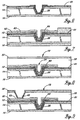
- Figure 2 illustrates the base substrate 10 after the copper within the exposed area 20 has been etched away. An exposed portion 22 of dielectric layer 14 is shown. The photoresist 18 may then be removed from the substrate.
- the exposed dielectric portion 22 is ablated away with a laser to define a "well" 24 into which a metallic contact will be formed, as shown in Figure 3.
- the copper layer 12 functions as a mask to permit ablation of the exposed dielectric portion 22.
- the copper layer 16 acts as a stop and will define the bottom of the well 24.
- the ablation of the exposed dielectric portion 22 may be accomplished by any laser suitable for selective ablation of organic dielectrics, without removing a copper layer.
- Lasers which operate in ultra violet wavelengths are particularly well suited, such as excimer lasers, and frequency tripled or quadrupled YAG lasers. However, other types of lasers are also suitable.
- the laser may be operated either in a scanning mode, in which the surface of the substrate is swept with a large laser spot, or in a focused beam.
- other processes may be employed to selectively remove the exposed dielectric portion 22, such as but not limited to plasma etching, reactive ion etching, or chemical etching.
- a laser ablation process is particularly well suited, as it permits more control over the shape of the well 24. Simple diffraction will provide a tapered conical shape in the case of scanning mode laser ablation process.
- the base substrate 10 is processed in any suitable manner which deposits a surface conductive layer 26, such as copper, on the side walls of the well 24.
- a surface conductive layer 26 such as copper
- Suitable processes include, but are not limited to a conventional electroless copper plating operation, sputtering, evaporation, or deposition of a conductive coating which allows direct etedrodeposition, or any other suitable process. Additional electrolytically deposited copper may be added to thicken this deposit, thereby providing a more robust surface for additional process steps.
- Figure 4 illustrates the base substrate 10 after this conductive deposition step.
- the base substrate is then coated with photoresist 28 on both sides of the base substrate, and the photoresist is processed to define patterns on conductive layer 12, into which solder 60 is deposited to simultaneously form at least one metal "bump" contact.
- solder include eutectic solder having a ratio of tin to lead of approximately 63/37% and having a melting point of about 180-185 degrees C.
- Figure 5 illustrates a substrate with the metals deposited as described.
- the photoresist 28 is removed from the base substrate 10.
- the base substrate 10 is then coated with an additional thin layer of copper 61 which is applied by sputtering or evaporation.
- the purpose of this copper layer is to allow additional plating over the solder deposit 60, which is normally oxidized and difficult to electroplate.
- the base substrate 10 is then coated with photoresist 28 on both sides, and the photoresist is processed to define patters on conductive layer 12, into which additional metal is deposited to simultaneously form the contact and the traces of the electric circuit.
- the pad around the contact would most often extend beyond the region into which solder 60 was deposited.
- a layer of nickel 62 or other metal, which would resist the flow of molten solder, is then deposited.
- a layer of copper 63 which will comprise the bulk of the metal, is then deposited.
- Figure 7 illustrates substrate with the metals deposited as described.
- the photoresist 28 is removed from the base substrate 10.
- the base substrate 10 may then be treated in a conventional oxide process, such as is common in the production of printed circuits.
- the rough oxide formed on the surface of the exposed copper of the base substrate will serve to provide adequate adhesion of the metal to a dielectric material in subsequent lamination processes.
- a layer of a dielectric prepreg material 33, and a "cap" layer of copper 32 is laminated onto the base substrate 10.
- the temperature, pressure, and time required for the lamination process should be as specified by the manufacturer of the particular dielectric prepeg used.
- resin from the dielectric prepreg material 33 will flow into and fill the void space remaining in the well 24.
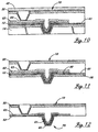
- Figure 9 illustrates a via 40 which is formed to interconnect the top conductive layer 32 to the conductive layer 12.
- Via 40 is formed used the same process as described for the formation of the well 24, except that the deposition of the solder and thin sputtered copper is not necessary.
- the top metal layer 32 of the base substrate is then coated with photoresist 42.
- Conductive layer 16 is then etched away using a suitable etchant.
- Figure 10 illustrates base substrate 10 after the bottom conductive layer 16 has been etched. The photoresist 42 is then removed from conductive layer 32.
- the now exposed dielectric material 14 is removed by any suitable process which will selectively remove dielectric from a conductor such as copper. Suitable processes include but are not limited to plasma etching, laser ablation reactive ion etching, or chemical etching. Care must be taken that all of the dielectric material 14 is removed from the conductive layer 12, as any remaining dielectric material 14 will prevent the conductive layer 12 from being etched away in subsequent process steps.
- Figure 11 depicts the base substrate 10 after the dielectric material 14 has been removed.
- the top layer of the base substrate 10 is then coated with photoresist to protect it from the etchant which is used to remove the exposed conductive layer 12 and surface conductive layers 26 and 61.
- etchant which is used to remove the exposed conductive layer 12 and surface conductive layers 26 and 61.
- Any suitable etchant may be employed, however, the etchant must be capable of removing the conductive copper layers 12, 26 and 61, but not the solder layer 60 and the nickel layer 62.
- An alkaline copper etchant consisting of a copper ammonium complex, ammonium chloride, ammonium hydroxide, sodium chlorite, ammonium bicarbonate, ammonium phosphate, and ammonium nitrate, and commonly referred to as alkaline or ammoniacal etchant is particularly well suited.
- the photoresist may then be removed from the circuit and the solder reflowed.
- a copper/nickel metallurgy remains to form the interconnecting traces, with copper/nickel/thin copper/solder metallurgy for a bump 70.
- the nickel, bearing a native oxide, will act to prevent flow of the solder onto the traces during subsequent reflow and chip attach.
- Figure 12 illustrates a finished circuit made in accordance with the teachings of one embodiment of the present invention.
- the height of the bump 70 is determined by the thickness of the dielectric layer 14, minus the sum of the thickness of the copper layer 12 and the surface conductive copper layer 24.
- the bump height is largely determined by the thickness of the dielectric layer 14.
- dielectrics available today offer thickness control of +/- 10% or better, thus the planarity of the bumps created will approach +/-10%.
- the ability to control the bump height by controlling the thickness of the dielectric layer 14, and the degree of planarity achievable by this method is a significant improvement over the method of etching depressions in a mandrel, as described in U.S. Patent 5.197,184.
- process steps are described which permit a base substrate 10, with raised metallic contacts 50, to be laminated and electrically connected to a mukilayer circuit board.
- the base substrate 10 is shown as made by the process steps which are described by Figures 1-7.
- the base substrate 10 is laminated to a multilayer circuit board 80 with a dielectric prepreg material, as best seen by reference to Figure 14.
- the temperature, pressure, and time required for the lamination process should be as specified by the manufacturer of the particular dielectric prepreg used.
- the multilayer circuit board may have any number of configurations. However, the side which is to be laminated to the base substrate 10 must have a series of pads 60 arranged such that vias 40 may later connect these pads to the base substrate 10, as best seen by sequentially viewing Figures 14-18.
- the opposite side of the multilayer circuit board may be finished prior to lamination, or may have only an unfinished copper layer, in which case this layer will be finished at the same time as the side with the raised contacts.
- the top metal layer of the multi-layer circuit board 80 is then coated with photoresist to protect it from an etchant which is used to etch the conductive layer 16 from the base substrate 10. Any suitable etchant may be used.
- the photoresist is then removed from the multi-layer circuit board 80.
- the now exposed dielectric material 14 is removed by any suitable process for removing a dielectric material from a conductor, such as copper, to thereby expose the raised metallic contacts 50, as best seen in Figure 15.
- a suitable process may include, but is not limited to a plasma etching process, laser ablation, reactive ion etching, or chemical etching, for example. Care must be taken to remove all of the dielectric material from the conductive surface, as any - remaining dielectric material will prevent the conductive material from being etched in subsequent process steps.
- the top layer of the multi-layer circuit board 80 is then coated with photoresist to protect it from the etchant which is used to remove the exposed conductive layer 12.
- etchant which is used to remove the exposed conductive layer 12.
- Any suitable etchant may be employed, however, the etchant must be capable of removing the conductive copper layers 12, 26 and 61, but not the solder layer 60 and the nickel layer 62.
- An alkaline copper etchant consisting of a copper ammonium complex, ammonium chloride, ammonium hydroxide, sodium chlorite, ammonium bicarbonate, ammonium phosphate, and ammonium nitrate, and commonly referred to as alkaline or ammoniacal etchant is particularly well suited.
- the photoresist may then be removed from the circuit and the solder reflowed.
- a copper/nickel metallurgy remains to form the interconnecting traces, with copper/nickel/thin copper/solder metallurgy for a bump 70.
- the nickel, bearing a native oxide, will act to prevent flow of the solder onto the traces during subsequent reflow and chip attach.
- Figure 15 illustrates a finished circuit made in accordance with the teachings of the present invention.
- Vias 40 are then drilled in the base substrate 10 for circuit interconnection. These vias may be either blind or through vias.
- the base substrate 10 is then processed in a conventional electroless copper plating operation such as is common in printed and flexible circuit manufacturing operations.
- the electroless copper deposits a layer of copper on the base substrate 10 and on the surface of the side walls of the vias. Additional electrolytically deposited copper may be added to thicken the deposit, and provide a more robust surface for additional process steps.
- Figure 16 illustrates the base substrate 10 after such copper deposition.
- any suitable process which deposits a conductor may be used in place of the electroless copper process, such as but not limited to sputtering, evaporation, or deposition of a conductive coating which allows direct electrodeposition.
- the base substrate is then coated with photoresist 28 on both sides, and the photoresist is processed to define patterns into which additional metal is deposited to form via and pad connections. Additional copper would likely be deposited. Also, a final etch resistant metal such as nickel, gold or solder may then be deposited.
- Figure 17 illustrates a base substrate with the metals deposited as described hereinabove. After deposition is complete, the photoresist 28 is removed from the base substrate.
- the base substrate 10 is then etched in a suitable copper etchant to remove the copper from the areas which were previously covered with photoresist.
- the circuit may then be routed from a panel.
- a completed substrate is shown in Figure 18.
Landscapes
- Engineering & Computer Science (AREA)
- Manufacturing & Machinery (AREA)
- Microelectronics & Electronic Packaging (AREA)
- Production Of Multi-Layered Print Wiring Board (AREA)
- Electric Connection Of Electric Components To Printed Circuits (AREA)
- Manufacturing Of Printed Circuit Boards (AREA)
- Wire Bonding (AREA)
- Manufacturing Of Printed Wiring (AREA)
Claims (7)
- Verfahren zum Bilden mindestens eines erhöhten metallischen Kontaktes auf einem elektrischen Schaltkreis, wobei das Verfahren die folgenden Schritte umfasst:Schaffen eines Verbundmaterialbasissubstrates (10), welche durch mindestens eine erste leitfähige Schicht (12), ein dielektrisches Material (14) und eine zweite leitfähige Schicht (16) definiert ist;Entfernen eines vorbestimmten Abschnittes der ersten leitfähigen Schicht (12), um das dielektrische Material (14) freizulegen;Entfernen des freigelegten Abschnittes (22) des dielektrischen Materials (14), bis zur zweiten leitfähigen Schicht (16), wodurch eine Vertiefung (24) gebildet wird;Abscheiden von mindestens einer Schicht aus Lotmaterial (60) auf mindestens Seitenwandabschnitten der Vertiefung (24);Abscheiden mindestens einer Schicht leitfähigen Materials (61) auf der Lotschicht (60);Entfernen der zweiten leitfähigen Schicht (16); undEntfernen des dielektrischen Materials (14), wodurch ein erhöhter metallischer Kontakt gebildet wird, der sich senkrecht von der ersten leitfähigen Schicht (12) fort erstreckt.
- Verfahren nach Anspruch 1, wobei das Verfahren ferner den folgenden Schritt aufweist:Laminieren mindestens eines zweiten dielektrischen Materials auf das Verbundwerkstoffbasissubstrat (10).
- Verfahren nach Anspruch 2, welches ferner den Schritt der Abscheidung einer dritten leitfähigen Schicht auf dem zweiten dielektrischen Material umfasst.
- Verfahren nach Anspruch 3, welches ferner die Schritte umfasst:Entfernen eines vorbestimmten Abschnittes der dritten leitfähigen Schicht, um einen Abschnitt des zweiten dielektrischen Materials freizulegen;Entfernen des freigelegten Abschnittes des zweiten dielektrischen Materials; undelektrisches Verbinden der dritten leitfähigen Schicht mit der ersten leitfähigen Schicht (12).
- Verfahren nach Anspruch 1, wobei die erste leitfähige Schicht (12) des Verbundwerkstoffbasissubstrates (10) durch mindestens eine erste Kupferschicht definiert ist, wobei die zweite leitfähige Schicht (16) durch eine zweite Kupferschicht definiert ist;
wobei das Verfahren ferner die Schritte aufweist:Abscheiden mindestens einer Materialschicht auf der leitfähigen Schicht, wobei das Material flüssigem oder geschmolzenem Lot widersteht; undLaminieren mindestens eines zweiten dielektrischen Materials auf die erste planare Oberfläche des Verbundwerkstoffbasissubstrates (10). - Verfahren nach Anspruch 5, welches nach dem Schritt der Abscheidung des Materials auf der leitfähigen Schicht ferner den zusätzlichen Schritt der Abscheidung von Kupfer auf dem Material umfasst.
- Verfahren nach den Ansprüchen 1, 2 oder 5, welches ferner den Schritt der Laminierung des Basissubstrates (10) auf eine Leiterplatte aufweist.
Applications Claiming Priority (5)
| Application Number | Priority Date | Filing Date | Title |
|---|---|---|---|
| US744842 | 1985-06-13 | ||
| US08/655,017 US5747358A (en) | 1996-05-29 | 1996-05-29 | Method of forming raised metallic contacts on electrical circuits |
| US655017 | 1996-05-29 | ||
| US08/744,842 US5786270A (en) | 1996-05-29 | 1996-11-08 | Method of forming raised metallic contacts on electrical circuits for permanent bonding |
| PCT/US1997/008012 WO1997046062A1 (en) | 1996-05-29 | 1997-05-08 | Method of forming raised metallic contacts on electrical circuits for permanent bonding |
Publications (2)
| Publication Number | Publication Date |
|---|---|
| EP0857403A1 EP0857403A1 (de) | 1998-08-12 |
| EP0857403B1 true EP0857403B1 (de) | 2005-07-27 |
Family
ID=27096874
Family Applications (1)
| Application Number | Title | Priority Date | Filing Date |
|---|---|---|---|
| EP97924676A Expired - Lifetime EP0857403B1 (de) | 1996-05-29 | 1997-05-08 | Verfahren und herstellung erhöhter metallischer kontakte auf elektrischen schaltungen für permanente verbindungen |
Country Status (5)
| Country | Link |
|---|---|
| EP (1) | EP0857403B1 (de) |
| JP (1) | JP3759755B2 (de) |
| AU (1) | AU3004097A (de) |
| DE (1) | DE69733801T2 (de) |
| WO (1) | WO1997046062A1 (de) |
Families Citing this family (3)
| Publication number | Priority date | Publication date | Assignee | Title |
|---|---|---|---|---|
| JP5653144B2 (ja) * | 2004-12-16 | 2015-01-14 | 新光電気工業株式会社 | 半導体パッケージの製造方法 |
| JP2007157620A (ja) * | 2005-12-08 | 2007-06-21 | D D K Ltd | 電気接点構造 |
| US10448517B2 (en) * | 2016-11-04 | 2019-10-15 | Jabil Inc. | Method and apparatus for flexible circuit cable attachment |
Family Cites Families (5)
| Publication number | Priority date | Publication date | Assignee | Title |
|---|---|---|---|---|
| US3319317A (en) * | 1963-12-23 | 1967-05-16 | Ibm | Method of making a multilayered laminated circuit board |
| US5024734A (en) * | 1989-12-27 | 1991-06-18 | Westinghouse Electric Corp. | Solder pad/circuit trace interface and a method for generating the same |
| US5197184A (en) * | 1990-09-11 | 1993-03-30 | Hughes Aircraft Company | Method of forming three-dimensional circuitry |
| US5072520A (en) * | 1990-10-23 | 1991-12-17 | Rogers Corporation | Method of manufacturing an interconnect device having coplanar contact bumps |
| US5326412A (en) * | 1992-12-22 | 1994-07-05 | Hughes Aircraft Company | Method for electrodepositing corrosion barrier on isolated circuitry |
-
1997
- 1997-05-08 WO PCT/US1997/008012 patent/WO1997046062A1/en not_active Ceased
- 1997-05-08 JP JP54247897A patent/JP3759755B2/ja not_active Expired - Lifetime
- 1997-05-08 AU AU30040/97A patent/AU3004097A/en not_active Abandoned
- 1997-05-08 EP EP97924676A patent/EP0857403B1/de not_active Expired - Lifetime
- 1997-05-08 DE DE69733801T patent/DE69733801T2/de not_active Expired - Lifetime
Also Published As
| Publication number | Publication date |
|---|---|
| JPH11509991A (ja) | 1999-08-31 |
| EP0857403A1 (de) | 1998-08-12 |
| JP3759755B2 (ja) | 2006-03-29 |
| DE69733801D1 (de) | 2005-09-01 |
| DE69733801T2 (de) | 2006-06-01 |
| WO1997046062A1 (en) | 1997-12-04 |
| AU3004097A (en) | 1998-01-05 |
Similar Documents
| Publication | Publication Date | Title |
|---|---|---|
| US5786270A (en) | Method of forming raised metallic contacts on electrical circuits for permanent bonding | |
| US8322030B1 (en) | Circuit-on-foil process for manufacturing a laminated semiconductor package substrate having embedded conductive patterns | |
| US5317801A (en) | Method of manufacture of multilayer circuit board | |
| US7670962B2 (en) | Substrate having stiffener fabrication method | |
| US8119516B2 (en) | Bump structure formed from using removable mandrel | |
| US5146674A (en) | Manufacturing process of a high density substrate design | |
| EP0997942A2 (de) | Chipgrosses Halbleitergehäuse und seine Herstellung | |
| JPH03211792A (ja) | 多層回路カード構造及びその製造方法 | |
| US6074567A (en) | Method for producing a semiconductor package | |
| GB2250381A (en) | Interconnect device having coplanar contact bumps and method of manufacture thereof | |
| EP0450381A2 (de) | Mehrschicht-Verbindungsstruktur | |
| US20090242238A1 (en) | Buried pattern substrate | |
| KR100857165B1 (ko) | 회로기판 제조방법 | |
| KR100315588B1 (ko) | 다층배선기판의제조방법 | |
| US6730859B2 (en) | Substrate for mounting electronic parts thereon and method of manufacturing same | |
| KR100339252B1 (ko) | 땜납범프(bump)를갖춘반도체장치및그의제조방법 | |
| US5843806A (en) | Methods for packaging tab-BGA integrated circuits | |
| CN1059982C (zh) | 制造集成电路封装电路板的方法 | |
| JP2003218490A (ja) | プリント配線板およびその製造方法 | |
| EP0857403A1 (de) | Verfahren und herstellung erhöhter metallischer kontakte auf elektrischen schaltungen für permanente verbindungen | |
| JP2001308484A (ja) | 回路基板及びその製造方法 | |
| US20040105955A1 (en) | Lamination process and structure of high layout density substrate | |
| KR100477258B1 (ko) | 범프의 형성방법 및 이로부터 형성된 범프를 이용한인쇄회로기판의 제조방법 | |
| KR20030071391A (ko) | 범프의 형성방법 및 이로부터 형성된 범프를 이용한인쇄회로기판의 제조방법 | |
| JP4401136B2 (ja) | 実装用回路基板とその製造方法 |
Legal Events
| Date | Code | Title | Description |
|---|---|---|---|
| PUAI | Public reference made under article 153(3) epc to a published international application that has entered the european phase |
Free format text: ORIGINAL CODE: 0009012 |
|
| 17P | Request for examination filed |
Effective date: 19971204 |
|
| AK | Designated contracting states |
Kind code of ref document: A1 Designated state(s): DE FR GB NL |
|
| 17Q | First examination report despatched |
Effective date: 20040903 |
|
| GRAP | Despatch of communication of intention to grant a patent |
Free format text: ORIGINAL CODE: EPIDOSNIGR1 |
|
| GRAS | Grant fee paid |
Free format text: ORIGINAL CODE: EPIDOSNIGR3 |
|
| GRAA | (expected) grant |
Free format text: ORIGINAL CODE: 0009210 |
|
| AK | Designated contracting states |
Kind code of ref document: B1 Designated state(s): DE FR GB NL |
|
| REG | Reference to a national code |
Ref country code: GB Ref legal event code: FG4D |
|
| REF | Corresponds to: |
Ref document number: 69733801 Country of ref document: DE Date of ref document: 20050901 Kind code of ref document: P |
|
| ET | Fr: translation filed | ||
| PLBE | No opposition filed within time limit |
Free format text: ORIGINAL CODE: 0009261 |
|
| STAA | Information on the status of an ep patent application or granted ep patent |
Free format text: STATUS: NO OPPOSITION FILED WITHIN TIME LIMIT |
|
| 26N | No opposition filed |
Effective date: 20060428 |
|
| REG | Reference to a national code |
Ref country code: FR Ref legal event code: PLFP Year of fee payment: 20 |
|
| PGFP | Annual fee paid to national office [announced via postgrant information from national office to epo] |
Ref country code: NL Payment date: 20160422 Year of fee payment: 20 |
|
| PGFP | Annual fee paid to national office [announced via postgrant information from national office to epo] |
Ref country code: DE Payment date: 20160421 Year of fee payment: 20 Ref country code: GB Payment date: 20160426 Year of fee payment: 20 |
|
| PGFP | Annual fee paid to national office [announced via postgrant information from national office to epo] |
Ref country code: FR Payment date: 20160422 Year of fee payment: 20 |
|
| REG | Reference to a national code |
Ref country code: DE Ref legal event code: R071 Ref document number: 69733801 Country of ref document: DE |
|
| REG | Reference to a national code |
Ref country code: NL Ref legal event code: MK Effective date: 20170507 |
|
| REG | Reference to a national code |
Ref country code: GB Ref legal event code: PE20 Expiry date: 20170507 |
|
| PG25 | Lapsed in a contracting state [announced via postgrant information from national office to epo] |
Ref country code: GB Free format text: LAPSE BECAUSE OF EXPIRATION OF PROTECTION Effective date: 20170507 |