EP0860740B1 - Material zur Herstellung von Feinstrukturen - Google Patents
Material zur Herstellung von Feinstrukturen Download PDFInfo
- Publication number
- EP0860740B1 EP0860740B1 EP98102927A EP98102927A EP0860740B1 EP 0860740 B1 EP0860740 B1 EP 0860740B1 EP 98102927 A EP98102927 A EP 98102927A EP 98102927 A EP98102927 A EP 98102927A EP 0860740 B1 EP0860740 B1 EP 0860740B1
- Authority
- EP
- European Patent Office
- Prior art keywords
- resist film
- polymer
- compound
- acid
- metal oxide
- Prior art date
- Legal status (The legal status is an assumption and is not a legal conclusion. Google has not performed a legal analysis and makes no representation as to the accuracy of the status listed.)
- Expired - Lifetime
Links
Images


Classifications
-
- G—PHYSICS
- G03—PHOTOGRAPHY; CINEMATOGRAPHY; ANALOGOUS TECHNIQUES USING WAVES OTHER THAN OPTICAL WAVES; ELECTROGRAPHY; HOLOGRAPHY
- G03F—PHOTOMECHANICAL PRODUCTION OF TEXTURED OR PATTERNED SURFACES, e.g. FOR PRINTING, FOR PROCESSING OF SEMICONDUCTOR DEVICES; MATERIALS THEREFOR; ORIGINALS THEREFOR; APPARATUS SPECIALLY ADAPTED THEREFOR
- G03F7/00—Photomechanical, e.g. photolithographic, production of textured or patterned surfaces, e.g. printing surfaces; Materials therefor, e.g. comprising photoresists; Apparatus specially adapted therefor
- G03F7/20—Exposure; Apparatus therefor
- G03F7/2022—Multi-step exposure, e.g. hybrid; backside exposure; blanket exposure, e.g. for image reversal; edge exposure, e.g. for edge bead removal; corrective exposure
-
- G—PHYSICS
- G03—PHOTOGRAPHY; CINEMATOGRAPHY; ANALOGOUS TECHNIQUES USING WAVES OTHER THAN OPTICAL WAVES; ELECTROGRAPHY; HOLOGRAPHY
- G03F—PHOTOMECHANICAL PRODUCTION OF TEXTURED OR PATTERNED SURFACES, e.g. FOR PRINTING, FOR PROCESSING OF SEMICONDUCTOR DEVICES; MATERIALS THEREFOR; ORIGINALS THEREFOR; APPARATUS SPECIALLY ADAPTED THEREFOR
- G03F7/00—Photomechanical, e.g. photolithographic, production of textured or patterned surfaces, e.g. printing surfaces; Materials therefor, e.g. comprising photoresists; Apparatus specially adapted therefor
- G03F7/004—Photosensitive materials
- G03F7/0045—Photosensitive materials with organic non-macromolecular light-sensitive compounds not otherwise provided for, e.g. dissolution inhibitors
-
- G—PHYSICS
- G03—PHOTOGRAPHY; CINEMATOGRAPHY; ANALOGOUS TECHNIQUES USING WAVES OTHER THAN OPTICAL WAVES; ELECTROGRAPHY; HOLOGRAPHY
- G03F—PHOTOMECHANICAL PRODUCTION OF TEXTURED OR PATTERNED SURFACES, e.g. FOR PRINTING, FOR PROCESSING OF SEMICONDUCTOR DEVICES; MATERIALS THEREFOR; ORIGINALS THEREFOR; APPARATUS SPECIALLY ADAPTED THEREFOR
- G03F7/00—Photomechanical, e.g. photolithographic, production of textured or patterned surfaces, e.g. printing surfaces; Materials therefor, e.g. comprising photoresists; Apparatus specially adapted therefor
- G03F7/004—Photosensitive materials
- G03F7/039—Macromolecular compounds which are photodegradable, e.g. positive electron resists
-
- G—PHYSICS
- G03—PHOTOGRAPHY; CINEMATOGRAPHY; ANALOGOUS TECHNIQUES USING WAVES OTHER THAN OPTICAL WAVES; ELECTROGRAPHY; HOLOGRAPHY
- G03F—PHOTOMECHANICAL PRODUCTION OF TEXTURED OR PATTERNED SURFACES, e.g. FOR PRINTING, FOR PROCESSING OF SEMICONDUCTOR DEVICES; MATERIALS THEREFOR; ORIGINALS THEREFOR; APPARATUS SPECIALLY ADAPTED THEREFOR
- G03F7/00—Photomechanical, e.g. photolithographic, production of textured or patterned surfaces, e.g. printing surfaces; Materials therefor, e.g. comprising photoresists; Apparatus specially adapted therefor
- G03F7/26—Processing photosensitive materials; Apparatus therefor
- G03F7/265—Selective reaction with inorganic or organometallic reagents after image-wise exposure, e.g. silylation
-
- G—PHYSICS
- G03—PHOTOGRAPHY; CINEMATOGRAPHY; ANALOGOUS TECHNIQUES USING WAVES OTHER THAN OPTICAL WAVES; ELECTROGRAPHY; HOLOGRAPHY
- G03F—PHOTOMECHANICAL PRODUCTION OF TEXTURED OR PATTERNED SURFACES, e.g. FOR PRINTING, FOR PROCESSING OF SEMICONDUCTOR DEVICES; MATERIALS THEREFOR; ORIGINALS THEREFOR; APPARATUS SPECIALLY ADAPTED THEREFOR
- G03F7/00—Photomechanical, e.g. photolithographic, production of textured or patterned surfaces, e.g. printing surfaces; Materials therefor, e.g. comprising photoresists; Apparatus specially adapted therefor
- G03F7/26—Processing photosensitive materials; Apparatus therefor
- G03F7/38—Treatment before imagewise removal, e.g. prebaking
-
- Y—GENERAL TAGGING OF NEW TECHNOLOGICAL DEVELOPMENTS; GENERAL TAGGING OF CROSS-SECTIONAL TECHNOLOGIES SPANNING OVER SEVERAL SECTIONS OF THE IPC; TECHNICAL SUBJECTS COVERED BY FORMER USPC CROSS-REFERENCE ART COLLECTIONS [XRACs] AND DIGESTS
- Y10—TECHNICAL SUBJECTS COVERED BY FORMER USPC
- Y10S—TECHNICAL SUBJECTS COVERED BY FORMER USPC CROSS-REFERENCE ART COLLECTIONS [XRACs] AND DIGESTS
- Y10S430/00—Radiation imagery chemistry: process, composition, or product thereof
- Y10S430/1053—Imaging affecting physical property or radiation sensitive material, or producing nonplanar or printing surface - process, composition, or product: radiation sensitive composition or product or process of making binder containing
- Y10S430/1055—Radiation sensitive composition or product or process of making
- Y10S430/106—Binder containing
-
- Y—GENERAL TAGGING OF NEW TECHNOLOGICAL DEVELOPMENTS; GENERAL TAGGING OF CROSS-SECTIONAL TECHNOLOGIES SPANNING OVER SEVERAL SECTIONS OF THE IPC; TECHNICAL SUBJECTS COVERED BY FORMER USPC CROSS-REFERENCE ART COLLECTIONS [XRACs] AND DIGESTS
- Y10—TECHNICAL SUBJECTS COVERED BY FORMER USPC
- Y10S—TECHNICAL SUBJECTS COVERED BY FORMER USPC CROSS-REFERENCE ART COLLECTIONS [XRACs] AND DIGESTS
- Y10S430/00—Radiation imagery chemistry: process, composition, or product thereof
- Y10S430/1053—Imaging affecting physical property or radiation sensitive material, or producing nonplanar or printing surface - process, composition, or product: radiation sensitive composition or product or process of making binder containing
- Y10S430/1055—Radiation sensitive composition or product or process of making
- Y10S430/106—Binder containing
- Y10S430/111—Polymer of unsaturated acid or ester
-
- Y—GENERAL TAGGING OF NEW TECHNOLOGICAL DEVELOPMENTS; GENERAL TAGGING OF CROSS-SECTIONAL TECHNOLOGIES SPANNING OVER SEVERAL SECTIONS OF THE IPC; TECHNICAL SUBJECTS COVERED BY FORMER USPC CROSS-REFERENCE ART COLLECTIONS [XRACs] AND DIGESTS
- Y10—TECHNICAL SUBJECTS COVERED BY FORMER USPC
- Y10S—TECHNICAL SUBJECTS COVERED BY FORMER USPC CROSS-REFERENCE ART COLLECTIONS [XRACs] AND DIGESTS
- Y10S430/00—Radiation imagery chemistry: process, composition, or product thereof
- Y10S430/1053—Imaging affecting physical property or radiation sensitive material, or producing nonplanar or printing surface - process, composition, or product: radiation sensitive composition or product or process of making binder containing
- Y10S430/1055—Radiation sensitive composition or product or process of making
- Y10S430/114—Initiator containing
- Y10S430/115—Cationic or anionic
-
- Y—GENERAL TAGGING OF NEW TECHNOLOGICAL DEVELOPMENTS; GENERAL TAGGING OF CROSS-SECTIONAL TECHNOLOGIES SPANNING OVER SEVERAL SECTIONS OF THE IPC; TECHNICAL SUBJECTS COVERED BY FORMER USPC CROSS-REFERENCE ART COLLECTIONS [XRACs] AND DIGESTS
- Y10—TECHNICAL SUBJECTS COVERED BY FORMER USPC
- Y10S—TECHNICAL SUBJECTS COVERED BY FORMER USPC CROSS-REFERENCE ART COLLECTIONS [XRACs] AND DIGESTS
- Y10S430/00—Radiation imagery chemistry: process, composition, or product thereof
- Y10S430/1053—Imaging affecting physical property or radiation sensitive material, or producing nonplanar or printing surface - process, composition, or product: radiation sensitive composition or product or process of making binder containing
- Y10S430/1055—Radiation sensitive composition or product or process of making
- Y10S430/114—Initiator containing
- Y10S430/12—Nitrogen compound containing
-
- Y—GENERAL TAGGING OF NEW TECHNOLOGICAL DEVELOPMENTS; GENERAL TAGGING OF CROSS-SECTIONAL TECHNOLOGIES SPANNING OVER SEVERAL SECTIONS OF THE IPC; TECHNICAL SUBJECTS COVERED BY FORMER USPC CROSS-REFERENCE ART COLLECTIONS [XRACs] AND DIGESTS
- Y10—TECHNICAL SUBJECTS COVERED BY FORMER USPC
- Y10S—TECHNICAL SUBJECTS COVERED BY FORMER USPC CROSS-REFERENCE ART COLLECTIONS [XRACs] AND DIGESTS
- Y10S430/00—Radiation imagery chemistry: process, composition, or product thereof
- Y10S430/1053—Imaging affecting physical property or radiation sensitive material, or producing nonplanar or printing surface - process, composition, or product: radiation sensitive composition or product or process of making binder containing
- Y10S430/1055—Radiation sensitive composition or product or process of making
- Y10S430/114—Initiator containing
- Y10S430/124—Carbonyl compound containing
-
- Y—GENERAL TAGGING OF NEW TECHNOLOGICAL DEVELOPMENTS; GENERAL TAGGING OF CROSS-SECTIONAL TECHNOLOGIES SPANNING OVER SEVERAL SECTIONS OF THE IPC; TECHNICAL SUBJECTS COVERED BY FORMER USPC CROSS-REFERENCE ART COLLECTIONS [XRACs] AND DIGESTS
- Y10—TECHNICAL SUBJECTS COVERED BY FORMER USPC
- Y10S—TECHNICAL SUBJECTS COVERED BY FORMER USPC CROSS-REFERENCE ART COLLECTIONS [XRACs] AND DIGESTS
- Y10S522/00—Synthetic resins or natural rubbers -- part of the class 520 series
- Y10S522/904—Monomer or polymer contains initiating group
Definitions
- the present invention relates to a method for forming a fine resist pattern in a process for fabricating a semiconductor integrated circuit (IC) device and the like (in this specification, such a method will be simply referred to as a "pattern forming method"), and also relates to a material for forming such a pattern used in the method (in a similar manner, such a material will be simply referred to as a "pattern forming material" in this specification).
- LSIs large-scale integrated circuits
- a pattern has been formed by a photolithography process using UV light.
- a light source utilizing a shorter wavelength has been used more and more frequently as the size of a semiconductor device has become increasingly small.
- a surface imaging process using a dry development technique has been developed in order to increase the focal depth and to improve a practical resolution.
- the surface imaging process is disclosed, for example, in United States Patent No. 5,278,029.
- the patent discloses a negative type surface modification process. Specifically, according to the disclosed process, first, a polysiloxane film is selectively formed on the surface of a resist film, which is made of a resist material generating an acid when the material is exposed to light. Thereafter, the resist film is dry-etched by using the polysiloxane film as a mask, thereby forming a resist pattern.
- a copolymer of 1,2,3,4-tetrahydronaphthylideneimino-p-styrene sulfonate (NISS) and methyl methacrylate (MMA) is assumed to be used as a resist material generating an acid when the material is exposed to light.
- a resist pattern is formed by performing the steps of: generating an acid in an exposed area of a resist film; selectively forming a metal oxide film in the exposed area by using the generated acid as a catalyst; and dry-etching the resist film by using the metal oxide film as a mask.
- this method is a negative type lithography process in which a resist pattern is formed in the exposed area of a resist film.
- the negative type lithography process has the following problems in, for example, forming contact holes for connecting multi-layer interconnections of an integrated circuit.
- the usage itself of a mask causes the following problems.
- the opening ratio of the mask becomes very high if the negative type lithography process is used as described above. Specifically, a light blocking film against the exposing radiation is formed only in the portions corresponding to the contact holes on the mask. On the other hand, the light blocking film is removed and quartz of the mask substrate is exposed in the portions other than the contact hole portions, because the former portions can transmit the exposing radiation.
- the ratio of the area occupied by all of the contact holes to the entire area of a semiconductor chip is very small.
- the opening ratio of the mask i.e., the ratio of the area occupied by the exposed quartz to the area of the light blocking film on the mask becomes very high.
- the process is much more likely to be affected by the contamination with ambient dust. More specifically, even when dust is adhered to the light blocking film portions of the mask, the dust hardly affects the process. However, if the dust is adhered to the transmissible portions of the mask, then these portions are turned into light blocking portions. When the exposure is performed by using such a mask to which dust has been adhered, pattern defects are caused in the portions to which the dust has been adhered and the portions corresponding thereto. As can be understood from the foregoing description, since the opening ratio of the mask becomes high in the negative type lithography process, the process is more likely to be affected by dust. As a result, this process has a problem in that the resulting yield is likely to decrease.
- the first and second problems described above are caused not only when the contact holes are formed, but also when a mask having a large light transmissible area is used and when the increase in focal depth is attempted.
- DE-A-4226464 describes a positive resist suitable for dry development containing
- EP-A-0425142 describes a positive photoresist composition capable of producing crosslinked images, which comprises a mixture of:
- a first patttern forming material comprising a compound which generates a base when the compound is irradiated with an energy beam characterized in that said material further comprises a polymer including a group which generates an acid when the polymer is heated, wherein said polymer is a binary polymer or a polymer of a higher degree, said polymer being obtained by polymerizing another compound with a compound which is represented by the following general formula (II): where R 1 indicates a hydrogen atom or an alkyl group, and R 4 indicates an alkyl group, an alkenyl group, a cyclic alkyl group or a cyclic alkenyl group.
- the present invention further relates to a second pattern forming material comprising a compound which generates a base when the compound is irradiated with a second energy beam having a second energy band which is different from a first energy band characterized in that said material further comprises a polymer including a group which generates an acid when the polymer is irradiated with a first energy beam having the first energy band.
- the first or the second pattern forming material is a mixture of a polymer including a group which generates an acid and a compound which generates a base, the polymer and the compound can be mixed at a more flexible ratio.
- the acid which has been generated from the polymer is neutralized with the base which has been generated from the compound.
- the acid which has been generated from the polymer is left and a metal alkoxide can be reacted by the catalyst function of the residual acid, thereby forming a metal oxide film.
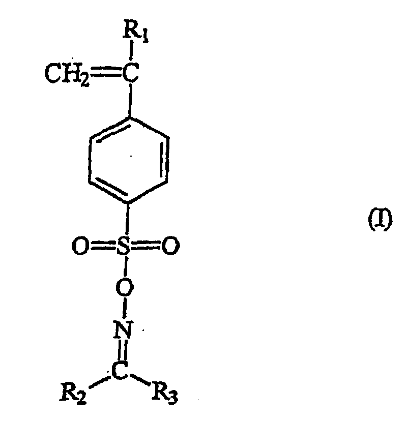
- the polymer is a binary polymer or a polymer of a higher degree obtained by polymerizing another group with a compound represented by the following general formula: where R 1 indicates a hydrogen atom or an alkyl group, and R 2 and R 3 independently indicate a hydrogen atom, an alkyl group, a phenyl group or an alkenyl group, or together indicate a cyclic alkyl group, a cyclic alkenyl group, a cyclic alkyl group having a phenyl group or a cyclic alkenyl group having a phenyl group.
- the ratio of the compound represented by Chemical Formula 1 to the binary polymer or the polymer of a higher degree may be set at an arbitrary value.
- the ratio is preferably equal to or lower than about 50 mol%.
- the polymer is a binary polymer or a polymer of a higher degree obtained by polymerizing another group with a compound represented by the following general formula: where R 1 indicates a hydrogen atom or an alkyl group, and R 4 indicates an alkyl group, an alkenyl group, a cyclic alkyl group or a cyclic alkenyl group.
- the compound represented by this general formula (Chemical Formula 2) is characterized by hardly generating an acid even when the compound is irradiated with light (or energy beam).
- the ratio of the compound represented by Chemical Formula 2 to the binary polymer or the polymer of a higher degree may be set at an arbitrary value. However, in order to facilitate the neutralization with the base, the ratio is preferably equal to or lower than about 50 mol%.
- the polymer is a binary polymer or a polymer of a higher degree obtained by polymerizing another group with the compound represented by the former general formula (Chemical Formula 1) in the second pattern forming material, or if the polymer is a binary polymer or a polymer of a higher degree obtained by polymerizing another group with the compound represented by the latter general formula (Chemical Formula 2) in the first pattern forming material, then sulfonic acid, generated from the polymer, functions as a strong catalyst when a metal oxide film is formed in the unexposed area of the resist film. As a result, a positive type surface modification process is realized at a high contrast.
- the compound is preferably acyloxime, a benzyloxycarbonyl compound or formamide.
- amine is generated in the exposed area of the resist film, and is strongly neutralized with the acid.
- a positive type surface modification process can be realized at a high contrast, illustrated in the following.
- the first pattern forming method includes: a first step of forming a resist film by coating a semiconductor substrate with a pattern forming material including a polymer having a group which generates an acid when the polymer is heated and a compound which generates a base when the compound is irradiated with an energy beam; a second step of generating the acid from the polymer by heating the resist film; a third step of irradiating the resist film with the energy beam through a mask having a desired pattern shape, generating the base from the compound in an exposed area of the resist film and thereby neutralizing the acid which has been generated from the polymer with the base which has been generated from the compound in the exposed area of the resist film; a fourth step of supplying a metal alkoxide onto the resist film and thereby forming a metal oxide film on a surface of an unexposed area of the resist film; and a fifth step of forming a resist pattern of the resist film by dry-etching the resist film by using the metal oxide film as a mask.
- the resist film when the resist film is heated, an acid is generated from the polymer over the entire surface of the resist film. Thereafter, when the resist film is exposed to the energy beam, a base is generated from the compound and the acid which has been generated from the polymer is neutralized with the base which has been generated from the compound in the exposed area of the resist film. On the other hand, in the unexposed area of the resist film, the acid is left. Next, when a metal alkoxide is supplied to the resist film, the metal alkoxide is reacted with the residual acid functioning as a catalyst to form a metal oxide film in the unexposed area of the resist film. On the other hand, since the exposed area of the resist film has been neutralized, no metal oxide film is formed therein.
- the metal oxide film is formed only in the unexposed area of the resist film thanks to the catalytic function of the acid.
- a fine resist pattern having a desired positive type pattern shape can be formed.
- the fourth step preferably includes a step of causing the unexposed area of the resist film to absorb water.
- the second pattern forming method includes: a first step of forming a resist film by coating a semiconductor substrate with a pattern forming material including a polymer having a group which generates an acid when the polymer is heated, and a compound which generates a base when the compound is irradiated with an energy beam; a second step of generating the base from the compound in an exposed area of the resist film by irradiating the resist film with the energy beam through a mask having a desired pattern shape; a third step of heating the resist film, generating the acid from the polymer and thereby neutralizing the base which has been generated from the compound with the acid which has been generated from the polymer in the exposed area of the resist film; a fourth step of supplying a metal alkoxide onto the resist film and forming a metal oxide film on a surface of an unexposed area of the resist film; and a fifth step of forming a resist pattern of the resist film by dry-etching the resist film by using the metal oxide film as a mask.
- the resist film when the resist film is exposed to the energy beam, a base is generated from the compound in the exposed area of the resist film. Thereafter, when the resist film is heated, an acid is generated from the polymer over the entire surface of the resist film. In the exposed area of the resist film, the base which has been generated from the compound is neutralized with the acid which has been generated from the polymer. On the other hand, in the unexposed area of the resist film, the acid is left. Next, when a metal alkoxide is supplied to the resist film, the metal alkoxide is reacted with the residual acid functioning as a catalyst to form a metal oxide film in the unexposed area of the resist film.
- the metal oxide film is formed only in the unexposed area of the resist film thanks to the catalytic function of the acid.
- a fine resist pattern having a desired positive type pattern shape can be formed.
- the fourth step preferably includes a step of causing the unexposed area of the resist film to absorb water.
- the third pattern forming method includes: a first step of forming a resist film by coating a semiconductor substrate with a pattern forming material including a compound which generates a base when the compound is irradiated with a first energy beam having a first energy band and a polymer which generates an acid when the polymer is irradiated with a second energy beam having a second energy band which is different from the first energy band; a second step of generating the base from the compound in an area of the resist film which has been exposed to the first energy beam by irradiating the resist film with the first energy beam through a mask having a desired pattern shape; a third step of irradiating an entire surface of the resist film with the second energy beam, generating the acid from the polymer over the entire surface of the resist film and thereby neutralizing the base which has been generated from the compound with the acid which has been generated from the polymer in the area of the resist film which has been exposed to the first energy beam; a fourth step of supplying a metal alkoxide onto the
- the third pattern forming method when the resist film is exposed to the first energy beam, a base is generated from the compound in the area of the resist film which has been exposed to the first energy beam. Thereafter, when the entire surface of the resist film is exposed to the second energy beam, an acid is generated from the polymer. In the area of the resist film which has been exposed to the first energy beam, the base which has been generated from the compound is neutralized with the acid which has been generated from the polymer. On the other hand, in the area of the resist film which has not been exposed to the first energy beam, the acid is left.
- the metal alkoxide is reacted with the residual acid functioning as a catalyst to form a metal oxide film in the area of the resist film which has not been exposed to the first energy beam.
- the area of the resist film, which has been exposed to the first energy beam has been neutralized, no metal oxide film is formed therein. That is to say, the metal oxide film is formed only in the area of the resist film which has not been exposed to the first energy beam thanks to the catalytic function of the acid.
- a fine resist pattern having a desired positive type pattern shape can be formed.
- the fourth step preferably includes a step of causing the area of the resist film, which has not been exposed to the first energy beam, to absorb water.
- the fourth pattern forming method includes: a first step of forming a resist film by coating a semiconductor substrate with a pattern forming material including a polymer which generates an acid when the polymer is irradiated with a first energy beam having a first energy band and a compound which generates a base when the compound is irradiated with a second energy beam having a second energy band which is different from the first energy band; a second step of generating the acid from the polymer in the resist film by irradiating an entire surface of the resist film with the first energy beam; a third step of irradiating the resist film with the second energy beam through a mask having a desired pattern shape, generating the base from the compound in an area of the resist film which has been exposed to the second energy beam and thereby neutralizing the acid which has been generated from the polymer with the base which has been generated from the compound in the area of the resist film which has been exposed to the second energy beam; a fourth step of supplying a metal alkoxide onto the resist film and
- the fourth pattern forming method when the entire surface of the resist film is exposed to the first energy beam, an acid is generated from the polymer over the entire surface of the resist film. Thereafter, when the resist film is exposed to the second energy beam, a base is generated from the compound and the acid which has been generated from the polymer is neutralized with the base which has been generated from the compound in the area of the resist film which has been exposed to the second energy beam. On the other hand, in the area of the resist film which has not been exposed to the second energy beam, the acid is left.
- the metal alkoxide is reacted with the residual acid functioning as a catalyst to form a metal oxide film in the area of the resist film which has not been exposed to the second energy beam.
- the area of the resist film which has been exposed to the second energy beam has been neutralized, no metal oxide film is formed therein. That is to say, the metal oxide film is formed only in the area of the resist film which has not been exposed to the second energy beam thanks to the catalytic function of the acid.
- a fine resist pattern having a desired positive type pattern shape can be formed.
- the fourth step preferably includes a step of causing the area of the resist film, which has not been exposed to the second energy beam, to absorb water.
- the polymer is a binary polymer or a polymer of a higher degree obtained by polymerizing another group with the compound represented by the following general formula where R 1 indicates a hydrogen atom or an alkyl group, and R 2 and R 3 independently indicate a hydrogen atom, an alkyl group, a phenyl group or an alkenyl group, or together indicate a cyclic alkyl group, a cyclic alkenyl group, a cyclic alkyl group having a phenyl group or a cyclic alkenyl group having a phenyl group.
- the ratio of the compound represented by this general formula (Chemical Formula 1) to the binary polymer or the polymer of a higher degree may be set at an arbitrary value. However, in order to facilitate the neutralization with the base, the ratio is preferably equal to or lower than about 50 mol%.
- the polymer is a binary polymer or a polymer of a higher degree obtained by polymerizing another group with a compound represented by the following general formula: where R 1 indicates a hydrogen atom or an alkyl group, and R 4 indicates an alkyl group, an alkenyl group, a cyclic alkyl group or a cyclic alkenyl group.
- the compound represented by this general formula (Chemical Formula 2) is characterized by hardly generating an acid even when the compound is irradiated with light (or energy beam).
- the ratio of the compound represented by this general formula (Chemical Formula 2) to the binary polymer or the polymer of a higher degree may be set at an arbitrary value. However, in order to facilitate the neutralization with the base, the ratio is preferably equal to or lower than about 50 mol%.
- Sulfonic acid functions as a strong catalyst when a metal oxide film is formed in the unexposed area of the resist film.
- a metal oxide film having a high selectivity can be formed only in the unexposed area of the resist film, and thus a more fine resist pattern having a desired positive type pattern shape can be formed.
- the compound which generates a base when it is irradiated with an energy beam is preferably acyloxime, a benzyloxycarbonyl compound or formamide.
- acyloxime may be O -phenylacetyl-aceto- ⁇ -naphtone-oxime, O -phenylacetyl-aceto- ⁇ -phenone-oxime, O -phenylacetyl-acetophenone-oxime.
- amine is generated in the exposed area of the resist film, and is strongly neutralized with the acid.
- a metal oxide film having a high selectivity can be formed only in the unexposed area of the resist film, and a more fine resist pattern having a desired positive type pattern shape can be formed.
- the fifth pattern forming method includes: a first step of forming a resist film by coating a semiconductor substrate with a pattern forming material including a polymer having a group which generates an acid when the polymer is heated and a compound which generates a base when the compound is irradiated with an energy beam; a second step of generating the acid from the polymer by heating the resist film; a third step of irradiating the resist film with the energy beam through a mask having a desired pattern shape so as to transfer the pattern, performing a water treatment on the resist film in a vapor phase or in a liquid phase, and thereby generating the base from the compound in an exposed area of the resist film and neutralizing the base which has been generated from the compound with the acid which has been generated from the polymer in the exposed area of the resist film; a fourth step of exposing the resist film to a water vapor environment and then to a mixed gas environment of water vapor and a metal alkoxide and thereby forming a metal oxide film on a surface of an
- the resist film, in which the acid has been generated is exposed to light
- a water treatment is performed on the resist film in a vapor phase or in a liquid phase.
- a sufficient amount of base for neutralizing the acid of the resist film is generated from the compound, so that the acid is not left.
- no metal oxide film is formed in the exposed area. Therefore, no residue of the metal oxide film is formed on the semiconductor substrate after a resist pattern has been formed thereon.
- the sixth pattern forming method includes: a first step of forming a resist film by coating a semiconductor substrate with a pattern forming material including a polymer having a group which generates an acid when the polymer is heated and a compound which generates a base when the compound is irradiated with an energy beam; a second step of generating the acid from the polymer by heating the resist film; a third step of irradiating the resist film with the energy beam through a mask having a desired pattern shape so as to transfer the pattern, retaining the resist film within an inert gas environment, and thereby generating the base from the compound in an exposed area of the resist film and neutralizing the base which has been generated from the compound with the acid which has been generated from the polymer in the exposed area of the resist film; a fourth step of exposing the resist film to a water vapor environment and then to a mixed gas environment of water vapor and a metal alkoxide and thereby forming a metal oxide film on a surface of an unexposed area of the resist film;
- the resist film in which an acid has been generated, is exposed to light, the resist film is retained within an inert gas environment.
- a sufficient amount of base for neutralizing the acid of the resist film is generated from the compound, so that the acid is not left.
- no metal oxide film is formed in the exposed area. Therefore, no residue of the metal oxide film is formed on the semiconductor substrate after a resist pattern has been formed thereon.
- the seventh pattern forming method includes: a first step of forming a resist film by coating a semiconductor substrate with a pattern forming material including a polymer having a group which generates an acid when the polymer is heated and a compound which generates a base when the compound is irradiated with an energy beam; a second step of generating the acid from the polymer by heating the resist film; a third step of irradiating the resist film with the energy beam through a mask having a desired pattern shape so as to transfer the pattern, exposing the resist film to a water vapor environment within an inert gas environment, and thereby generating the base from the compound in an exposed area of the resist film and neutralizing the base which has been generated from the compound with the acid which has been generated from the polymer in the exposed area of the resist film; a fourth step of exposing the resist film to a mixed gas environment of water vapor and a metal alkoxide and thereby forming a metal oxide film on a surface of an unexposed area of the resist film; and
- the resist film in which an acid has been generated, is exposed to light
- the resist film is exposed to a water vapor environment within an inert gas environment.
- a sufficient amount of base for neutralizing the acid of the resist film is generated from the compound, and the acid is not left.
- no metal oxide film is formed in the exposed area. Therefore, no residue of the metal oxide film is formed on the semiconductor substrate after a resist pattern has been formed thereon.
- the resist film is exposed to a water vapor environment within an inert gas environment, it is possible to omit the step of exposing the resist film to a water vapor environment, which step is to be performed before the step of exposing the resist film to a mixed gas environment of water vapor and a metal alkoxide is performed.
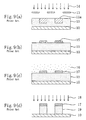
- Figures 2(a) through 2(d) are cross-sectional views showing the respective process steps of a pattern forming method in the first or the second embodiment.
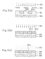
- Figures 3(a) through 3(c) are cross-sectional views showing the preceding process steps of a pattern forming method in the third embodiment.
- Figures 4(a) and 4(b) are cross-sectional views showing the succeeding process steps of the pattern forming method in the third embodiment.
- Figures 9(a) through 9(d) are cross-sectional views showing the respective process steps of a conventional pattern forming method.
- Figures 2(a) through 2(d) are cross-sectional views showing the respective process steps of a pattern forming method in the second embodiment of the present invention.
- Chemical Formula 7 i.e., a polymer including a group which generates an acid when the polymer is heated
- Chemical Formula 8 i.e., a compound which generates a base when the compound is irradiated with an energy beam (an ArF excimer laser beam)
- the resist material is spin-coated onto a semiconductor substrate 200 made of silicon and the coated semiconductor substrate is pre-baked at a temperature of about 120°C for about 90 seconds, thereby forming a resist film 201 having a thickness of about 1 ⁇ m. At this point, no peeling is observed and the resist film 201 shows satisfactory adhesion.
- sulfonic acid is generated from the copolymer represented by Chemical Formula 7 because of the heat generated by the pre-baking.
- the resist film 201 is irradiated with an ArF excimer laser beam 204 as an energy beam, thereby transferring the pattern of the mask 203 onto the resist film 201 .
- O -phenylacetyl-acetophenone-oxime is decomposed to generate benzylamine on the surface of an exposed area 201a of the resist film 201 , as represented by the chemical reaction in Chemical Formula 10.
- An unexposed area 201b of the resist film 201 shows strong acidic properties owing to the function of a sulfonic acid group shown in Chemical Formula 9.
- O -phenylacetyl-acetophenone-oxime is decomposed to generate benzylamine having basic properties as represented by the chemical reaction in Chemical Formula 10. Since benzylamine cancels the acidic properties resulting from the function of the sulfonic acid group, a neutralization proceeds to a certain degree.
- the unexposed area 201b of the resist film 201 shows the strong acidic properties
- water is more easily adsorbed into the unexposed area 201b as compared with the exposed area 201a which has been neutralized.
- a group having strong acidic properties exists in the unexposed area 201b
- hydrogen bonding with water is strengthened in the unexposed area 201b and thus water is more likely to be absorbed thereto.
- the exposed area 201a hydrogen bonding with water is weakened by the neutralization and thus water is less likely to be absorbed thereto.
- the semiconductor substrate 200 is retained in the air having a relative humidity of about 95% at a temperature of about 30°C for about 30 minutes, thereby supplying water vapor 205 onto the surface of the resist film 201 .
- water vapor 205 is adsorbed into the surface of the unexposed area 201b , into which water is more likely to be adsorbed, and the adsorbed water diffuses into a deep level, for example, at a depth of about 100 nm from the surface of the unexposed area 201b . Since the exposed area 201a has been neutralized, water is less likely to be adsorbed thereto. As a result, a water-adsorbing layer 206 is selectively formed in the unexposed area 201b .
- vapor 207 of methyltrimethoxysilane is sprayed as a metal alkoxide onto the surface of the resist film 201 for about 20 minutes.
- a metal oxide film 208 is selectively formed on the surface of the unexposed area 201b of the resist film 201 .
- the acid (H + ) derived from sulfonic acid works as a catalyst to produce the hydrolysis and the dehydration of MTMOS, thereby forming the metal oxide film 208 . Therefore, the metal oxide film 208 grows only in the area where both the acid (H + ) serving as the catalyst and water exist.
- no metal oxide film is formed in the exposed area 201a of the resist film 201 because sulfonic acid is neutralized by the generated benzylamine and loses its function as a catalyst and because water is less likely to be absorbed thereto.
- the metal oxide film 208 is formed in the unexposed area 201b of the resist film 201 because H + serving as a catalyst exists there and a sufficient amount of water has been absorbed thereto.
- an RIE (reactive ion etching) process is performed by using O 2 plasma 209 , thereby forming a resist pattern 210 .
- the RIE process using O 2 plasma is performed by using a parallel plate RIE system under the conditions where a power of about 900 W is supplied, a pressure of about 0.7 Pa is applied and a flow rate is set at about 40 SCCM.
- a positive type resist pattern 210 having a vertical cross-sectional shape and a width of about 0.15 ⁇ m can be formed in the unexposed area 201b .
- MTMOS is supplied to the resist film 201 in the air having a relative humidity of about 95% in the process step shown in Figure 2(c) .
- the equilibrium of water can be maintained. This is because it is possible to prevent the water, which has been absorbed into the resist film 201 , from evaporating therefrom and because a sufficient amount of water required for forming the metal oxide film 208 can be supplied thereto. As a result, a metal oxide film 208 thick enough to withstand the RIE process using O 2 plasma can be formed.
- the resist film 201 in which an acid has been generated from the copolymer through a heat treatment, is exposed to light.
- a base is generated to neutralize the acidic properties of the exposed area 201a
- the metal oxide film 208 is selectively formed only in the unexposed area 201b .
- the resist film 201 is etched.
- MTMOS is used as a metal alkoxide.
- any other metal alkoxide such as CH 3 Si(OC 2 H 5 ) 3 (methyltriethoxysilane), Si(OCH 3 ) 4 (tetramethoxysilane), Si(OC 2 H 5 ) 4 (tetraethoxysilane), Ti(OC 2 H 5 ) 4 , Ge(OC 2 H 5 ) 4 , Al(OC 2 H 5 ) 3 or Zr(OC 2 H 5 ) 3 may be supplied in a vapor phase or in a liquid phase.
- the dry development is performed by the RIE process using O 2 plasma in this embodiment.
- an ECR (electron cyclotron resonance) etching process using O 2 plasma may be performed.
- a mixture gas in which SO 2 gas or the like is added to O 2 gas may be used as an alternative etching gas.
- the exposing radiation is assumed to be an ArF excimer laser beam in this embodiment.
- an i-beam, a KrF excimer laser beam, VUV, EUV, EB, an X-ray or the like may also be used.
- the semiconductor substrate 200 is retained within water vapor in this embodiment.
- water in a liquid phase may be supplied to the resist film 201 on the semiconductor substrate 200 .
- water can be more rapidly diffused and the depth of the metal oxide film 208 can be increased when water is supplied in a vapor phase than in a liquid phase.
- water is preferably supplied in a vapor phase.
- Figures 2(a) through 2(d) are cross-sectional views showing the respective process steps of a pattern forming method in the third embodiment of the present invention.
- a copolymer represented by Chemical Formula 11 i.e., a polymer including a group which generates an acid when the polymer is heated
- Chemical Formula 12 i.e., a compound which generates a base when the compound is irradiated with an energy beam (an ArF excimer laser beam)
- the resist material is spin-coated onto a semiconductor substrate 200 made of silicon and the coated semiconductor substrate is pre-baked at a temperature of about 80°C for about 90 seconds, thereby forming a resist film 201 having a thickness of about 1 ⁇ m. At this point, no peeling is observed and the resist film 201 shows satisfactory adhesion. During this pre-baking process, no acid is generated from the copolymer represented by Chemical Formula 11.
- the resist film 201 is irradiated with an ArF excimer laser beam 204 as an energy beam, thereby transferring the pattern of the mask 203 onto the resist film 201 .
- O -phenylacetyl-acetonaphtone-oxime is decomposed to generate benzylamine on the surface of an exposed area 201a of the resist film 201 .
- a pre-baking process is performed on the resist film 201 for about 90 seconds at a temperature of about 120°C.
- sulfonic acid is generated from the copolymer represented by Chemical Formula 11 because of the heat generated by the pre-baking process.
- An unexposed area 201b of the resist film 201 shows strong acidic properties owing to the function of a sulfonic acid group shown in Chemical Formula 13.
- O -phenylacetyl-acetonaphtone-oxime is decomposed to generate benzylamine having basic properties. Since benzylamine cancels the acidic properties resulting from the function of the sulfonic acid group, a neutralization proceeds to a certain degree.
- the unexposed area 201b of the resist film 201 shows the strong acidic properties
- water is more easily adsorbed into the unexposed area 201b as compared with the exposed area 201a which has been neutralized.
- a group having strong acidic properties exists in the unexposed area 201b
- hydrogen bonding with water is strengthened in the unexposed area 201b and thus water is more likely to be absorbed thereto.
- the exposed area 201a hydrogen bonding with water is weakened by the neutralization and thus water is less likely to be absorbed thereto.
- the semiconductor substrate 200 is retained in the air having a relative humidity of about 95% at a temperature of about 30°C for about 30 minutes, thereby supplying water vapor 205 onto the surface of the resist film 201 .
- water vapor 205 is adsorbed into the surface of the unexposed area 201b , into which water is more likely to be adsorbed, and the adsorbed water diffuses into a deep level, for example, at a depth of about 100 nm from the surface of the unexposed area 201b . Since the exposed area 201a has been neutralized, water is less likely to be adsorbed thereto. As a result, a water-adsorbing layer 206 is selectively formed in the unexposed area 201b .
- vapor 207 of methyltrimethoxysilane is sprayed as a metal alkoxide onto the surface of the resist film 201 for about 20 minutes.
- a metal oxide film 208 is selectively formed on the surface of the unexposed area 201b of the resist film 201 .
- the acid (H + ) derived from sulfonic acid works as a catalyst to produce the hydrolysis and the dehydration of MTMOS, thereby forming the metal oxide film 208 . Therefore, the metal oxide film 208 grows only in the area where both the acid (H + ) serving as the catalyst and water exist.
- no metal oxide film is formed in the exposed area 201a of the resist film 201 because sulfonic acid is neutralized by the generated benzylamine and loses its function as a catalyst and because water is less likely to be absorbed thereto.
- the metal oxide film 208 is formed in the unexposed area 201b of the resist film 201 because H + serving as a catalyst exists there and a sufficient amount of water has been absorbed thereto.
- an RIE (reactive ion etching) process is performed by using O 2 plasma 209 , thereby forming a resist pattern 210 .
- the RIE process using O 2 plasma is performed by using a parallel plate RIE system under the conditions where a power of about 900 W is supplied, a pressure of about 0.7 Pa is applied and a flow rate is set at about 40 SCCM.
- a positive type resist pattern 210 having a vertical cross-sectional shape and a width of about 0.15 ⁇ m can be formed in the unexposed area 201b .
- MTMOS is supplied to the resist film 201 in the air having a relative humidity of about 95% in the process step shown in Figure 2(c) .
- the equilibrium of water can be maintained. This is because it is possible to prevent the water, which has been absorbed into the resist film 201 , from evaporating therefrom and because a sufficient amount of water required for forming the metal oxide film 208 can be supplied thereto. As a result, a metal oxide film 208 thick enough to withstand the RIE process using O 2 plasma can be formed.
- the resist film 201 is exposed to light, thereby generating a base in the exposed area 201a . Thereafter, an acid is generated from the copolymer by heating the film, thereby neutralizing the basic properties of the exposed area 201a , while the metal oxide film 208 is selectively formed only in the unexposed area 201b . Then, by using the metal oxide film 208 as a mask, the resist film 201 is etched. Thus, it is possible to form a positive type fine resist pattern 210 having a desired shape.
- MTMOS is used as a metal alkoxide.
- any other metal alkoxide such as CH 3 Si(OC 2 H 5 ) 3 (methyltriethoxysilane), Si(OCH 3 ) 4 (tetramethoxysilane), Si(OC 2 H 5 ) 4 (tetraethoxysilane), Ti(OC 2 H 5 ) 4 , Ge(OC 2 H 5 ) 4 , Al(OC 2 H 5 ) 3 or Zr(OC 2 H 5 ) 3 may be supplied in a vapor phase or in a liquid phase.
- the dry development is performed by the RIE process using O 2 plasma in this embodiment.
- an ECR (electron cyclotron resonance) etching process using O 2 plasma may be performed.
- a mixture gas in which SO 2 gas or the like is added to O 2 gas may be used as an alternative etching gas.
- the exposing radiation is assumed to be an ArF excimer laser beam in this embodiment.
- an i-beam, a KrF excimer laser beam, VUV, EUV, EB, an X-ray or the like may also be used.
- the semiconductor substrate 200 is retained within water vapor in this embodiment.
- water in a liquid phase may be supplied to the resist film 201 on the semiconductor substrate 200 .
- water can be more rapidly diffused and the depth of the metal oxide film 208 can be increased when water is supplied in a vapor phase than in a liquid phase.
- water is preferably supplied in a vapor phase.
- Figures 3(a) through 3(a) and Figures 4(a) and 4(b) are cross-sectional views showing the respective process steps of a pattern forming method in the fourth embodiment of the present invention.
- Chemical Formula 14 i.e., a polymer including a group which generates an acid when the polymer is irradiated with the second energy beam (an i-beam)
- Chemical Formula 15 i.e., a compound which generates a base when the compound is irradiated with the first energy beam (an ArF excimer laser beam)
- the resist material is spin-coated onto a semiconductor substrate 300 made of silicon, and the coated semiconductor substrate is heated at a temperature of about 90°C for about 90 seconds, thereby forming a resist film 301 having a thickness of about 1 ⁇ m. At this point, no peeling is observed, and the resist film 301 shows satisfactory adhesion.
- the resist film 301 is irradiated with an ArF excimer laser beam 304 as the first energy beam, thereby transferring the pattern of the mask 303 onto the resist film 301 .
- O -tertiary butylacetyl-acetophenone-oxime is decomposed to generate amine on the surface of an exposed area 301a of the resist film 301 , as represented by the chemical reaction in Chemical Formula 16.
- the entire surface of the resist film 301 is exposed to an i-beam 305 as the second energy beam.
- sulfonic acid having acidic properties is generated in accordance with the exposure of the entire surface of the resist film 301 to the i-beam 305 , as represented by the chemical reaction in Chemical Formula 17.
- the exposed area 301a is neutralized.
- the unexposed area 301b of the resist film 301 which has not been exposed to the ArF excimer laser beam 304 , shows acidic properties, because sulfonic acid is generated therein in accordance with the exposure of the entire surface of the resist film 301 to the i-beam 305 , as represented by the chemical reaction in Chemical Formula 17.
- the unexposed area 301b shows strong acidic properties, water is more likely to be adsorbed thereto, as compared with the exposed area 301a which has been neutralized.
- the semiconductor substrate 300 is retained within the air having a relative humidity of about 95% at a temperature of about 30°C for about 30 minutes, thereby supplying water vapor 307 onto the surface of the resist film 301 .
- water vapor 307 is adsorbed into the surface of the unexposed area 301b , into which water is more likely to be adsorbed, and the adsorbed water diffuses into a deep level, for example, at a depth of about 100 nm from the surface of the unexposed area 301b . Since the exposed area 301a has been neutralized, water is less likely to be adsorbed thereto. As a result, a water-adsorbing layer 308 is selectively formed in the unexposed area 301b .
- vapor 309 of methyltriethoxysilane is sprayed as a metal alkoxide onto the surface of the resist film 301 for about 30 minutes.
- a metal oxide film 310 is selectively formed on the surface of the unexposed area 301b of the resist film 301 .
- an acid (H + ) derived from sulfonic acid works as a catalyst to produce the hydrolysis and the dehydration of MTEOS, thereby forming the metal oxide film 310 . Therefore, the metal oxide film 310 is formed only in the area where both the acid (H + ) serving as the catalyst and water exist.
- no metal oxide film is formed in the exposed area 301a of the resist film 301 because amine is neutralized by the generated sulfonic acid and loses its function as a catalyst and because water is less likely to be absorbed thereto.
- the metal oxide film 310 is formed in the unexposed area 301b of the resist film 301 because the acid serving as the catalyst exists there and a sufficient amount of water has been absorbed thereto.
- an RIE (reactive ion etching) process is performed by using O 2 plasma 311 , thereby forming a resist pattern 312 .
- the RIE process using O 2 plasma is performed by using a parallel plate RIE system under the conditions where a power of about 900 W is supplied, a pressure of about 0.7 Pa is applied and a flow rate is set at about 40 SCCM.
- a positive type resist pattern 312 having a vertical cross-sectional shape and a width of about 0.15 ⁇ m can be formed in the unexposed area 301b .
- the resist film 301 is exposed to the first energy beam, thereby generating a base in the exposed area 301a . Thereafter, the entire surface of the resist film 301 is exposed to the second energy beam, thereby generating an acid and neutralizing the exposed area 301a which has been subjected to an exposure. On the other hand, the unexposed area 301b is acidified, thereby selectively forming the metal oxide film 310 only in the unexposed area 301b . And then the resist film 301 is etched by using the metal oxide film 310 as a mask. Thus, it is possible to form a positive type fine resist pattern 312 having a desired shape.
- MTEOS is used as a metal alkoxide.
- any other metal alkoxide such as CH 3 Si(OCH 3 ) 3 (methyltrimethoxysilane), Si(OCH 3 ) 4 (tetramethoxysilane), Si(OC 2 H 5 ) 4 (tetraethoxysilane), Ti(OC 2 H 5 ) 4 , Ge(OC 2 H 5 ) 4 , Al(OC 2 H 5 ) 3 or Zr(OC 2 H 5 ) 3 may be supplied in a vapor phase or in a liquid phase.
- the dry development is performed by the RIE process using O 2 plasma in this embodiment.
- an ECR (electron cyclotron resonance) etching process using O 2 plasma may be performed.
- a mixture gas in which SO 2 gas or the like is added to O 2 gas may be used as an alternative etching gas.
- the exposing radiation is assumed to be an ArF excimer laser beam in this embodiment.
- an i-beam, a KrF excimer laser beam, VUV, EUV, EB, an X-ray or the like may also be used.
- the semiconductor substrate 300 is retained within water vapor in this embodiment.
- water in a liquid phase may be supplied to the resist film 301 on the semiconductor substrate 300 .
- water can be more rapidly diffused and the depth of the metal oxide film 310 can be increased when water is supplied in a vapor phase than in a liquid phase.
- water is preferably supplied in a vapor phase.
- a mixture of a polymer e.g., a copolymer represented by Chemical Formula 14
- a compound e.g., a compound represented by Chemical Formula 15
- the second energy beam e.g., ArF excimer laser beam
- the entire surface of a resist film is exposed to the first energy beam, thereby generating an acid from the copolymer.
- the resist film is exposed to the second energy beam, thereby generating a base in the area of the resist film which has been exposed to the second energy beam.
- the acid which has been generated from the copolymer is neutralized with the base which has been generated from the compound.
- a positive type fine resist pattern having a desired shape can also be formed in the same way as in the first to the fourth embodiments.
- a copolymer represented by Chemical Formula 7 a copolymer represented by Chemical Formula 11 and a copolymer represented by Chemical Formula 14 are used as the respective polymers.
- any other copolymer, such as those represented by Chemical Formulae 18 to 24, including a group which generates sulfonic acid may also be used.
- the ratio of the group which generates sulfonic acid to the copolymer may be set at an arbitrary value. However, in order to facilitate the neutralization with the base, the ratio is preferably equal to or lower than about 50 mol%.
- any compound, such as those represented by Chemical Formulae 25 to 30, including a group which generates amine may be used as the compound which generates a base.
- a compound which generates a group having basic properties may also be used instead of the compound including a group which generates amine.
- the exposing radiation for the exposure with the first energy beam is assumed to be an ArF excimer laser beam.
- an i-beam, a KrF excimer laser beam, EB, an X-ray may also be used.
- the selectivity of the metal oxide film functioning as a surface modification film is not satisfactory, some residue of the metal oxide film is adversely formed on the semiconductor substrate on which the resist pattern has been formed.
- the first reaction i.e., a radical decomposition
- O -phenylacetyl-acetophenone-oxime is decomposed into Radical a , CO 2 and Radical b .
- Radicals a and b are recombined.
- the third reaction i.e., a hydrolysis with water in the air, occurs, thereby producing benzylamine.
- the present inventors In order to reduce the amount of the residue by increasing the amount of the base (OH - ) generated in the unexposed area of the resist film, the present inventors repeatedly conducted experiments by increasing the amount of the ArF excimer laser beam as the exposing radiation. However, the residue could not be totally eliminated from the surface of the semiconductor substrate.
Landscapes
- Physics & Mathematics (AREA)
- General Physics & Mathematics (AREA)
- Spectroscopy & Molecular Physics (AREA)
- Chemical & Material Sciences (AREA)
- Chemical Kinetics & Catalysis (AREA)
- Inorganic Chemistry (AREA)
- Organic Chemistry (AREA)
- Photosensitive Polymer And Photoresist Processing (AREA)
- Exposure And Positioning Against Photoresist Photosensitive Materials (AREA)
- Materials For Photolithography (AREA)
Claims (4)
- Musterformendes Material, umfassend:worin R1 ein Wasserstoffatom oder eine Alkylgruppe angibt und R4 eine Alkylgruppe, eine Alkenylgruppe, eine zyklische Alkylgruppe oder eine zyklische Alkenylgruppe angibt.eine Verbindung, die eine Base erzeugt wenn die Verbindung mit einem Energiestrahl bestrahlt wird, dadurch gekennzeichnet, dass besagtes Material weiter ein Polymer enthält, umfassend eine Gruppe die eine Säure erzeugt, wenn das Polymer erwärmt wird, wobei besagtes Polymer ein binäres Polymer oder ein Polymer eines höheren Grades ist, wobei besagtes Polymer erhalten wird durch Polymerisieren einer weiteren Verbindung mit einer Verbindung, dargestellt durch die folgende allgemeine Formel (II):

- Musterformendes Materials, umfassend:eine Verbindung, die eine Base erzeugt wenn die Verbindung mit einem zweiten Energiestrahl bestrahlt wird, mit einem zweiten Energieband, verschieden von einem ersten Energieband, dadurch gekennzeichnet, dass besagtes Material weiter ein Polymer enthält, umfassend eine Gruppe die eine Säure erzeugt, wenn das Polymer mit einem ersten Energiestrahl mit dem ersten Energieband bestrahlt wird.
- Musterformendes Material nach Anspruch 2, wobei besagtes Polymer ein binäres Polymer oder ein Polymer eines höheren Grades ist, wobei besagtes Polymer erhalten wird durch Polymerisieren einer weiteren Verbdingung mit einer Verbindung, dargestellt durch die folgende allgemeine Formel (I):worin R1 ein Wasserstoffatom oder eine Alkylgruppe angibt, und R2 und R3 unabhängig voneinander ein Wasserstoffatom, eine Alkylgruppe, eine Phenylgruppe oder eine Alkenylgruppe angeben, oder diese zusammengenommen eine zyklische Alkylgruppe, eine zyklische Alkenylgruppe, eine zyklische Alkylgruppe mit einer Phenylgruppe oder eine zyklische Alkenylgruppe mit einer Phenylgruppe angeben.
- Musterformendes Material nach Anspruch 1 oder 2, wobei die Verbindung, die eine Base erzeugt wenn das Material mit einem Energiestrahl bestrahlt wird Acyloxim, eine Benzyloxycarbonylverbindung oder Formamid ist.
Priority Applications (1)
| Application Number | Priority Date | Filing Date | Title |
|---|---|---|---|
| EP00105601A EP1028353A1 (de) | 1997-02-20 | 1998-02-19 | Verfahren zur Herstellung von Mustern |
Applications Claiming Priority (9)
| Application Number | Priority Date | Filing Date | Title |
|---|---|---|---|
| JP3655197 | 1997-02-20 | ||
| JP3655197 | 1997-02-20 | ||
| JP36551/97 | 1997-02-20 | ||
| JP221724/97 | 1997-08-18 | ||
| JP22172497 | 1997-08-18 | ||
| JP22172497 | 1997-08-18 | ||
| JP230098 | 1998-01-08 | ||
| JP230098 | 1998-01-08 | ||
| JP2300/98 | 1998-01-08 |
Related Child Applications (1)
| Application Number | Title | Priority Date | Filing Date |
|---|---|---|---|
| EP00105601A Division EP1028353A1 (de) | 1997-02-20 | 1998-02-19 | Verfahren zur Herstellung von Mustern |
Publications (2)
| Publication Number | Publication Date |
|---|---|
| EP0860740A1 EP0860740A1 (de) | 1998-08-26 |
| EP0860740B1 true EP0860740B1 (de) | 2002-05-29 |
Family
ID=27275289
Family Applications (2)
| Application Number | Title | Priority Date | Filing Date |
|---|---|---|---|
| EP98102927A Expired - Lifetime EP0860740B1 (de) | 1997-02-20 | 1998-02-19 | Material zur Herstellung von Feinstrukturen |
| EP00105601A Ceased EP1028353A1 (de) | 1997-02-20 | 1998-02-19 | Verfahren zur Herstellung von Mustern |
Family Applications After (1)
| Application Number | Title | Priority Date | Filing Date |
|---|---|---|---|
| EP00105601A Ceased EP1028353A1 (de) | 1997-02-20 | 1998-02-19 | Verfahren zur Herstellung von Mustern |
Country Status (3)
| Country | Link |
|---|---|
| US (2) | US6017683A (de) |
| EP (2) | EP0860740B1 (de) |
| DE (1) | DE69805559T2 (de) |
Families Citing this family (24)
| Publication number | Priority date | Publication date | Assignee | Title |
|---|---|---|---|---|
| EP1124158A1 (de) * | 1996-02-26 | 2001-08-16 | Matsushita Electric Industrial Co., Ltd. | Bilderzeugungsmaterial und Verfahren |
| US6576392B1 (en) * | 1996-12-07 | 2003-06-10 | Fuji Photo Film Co., Ltd. | Positive photoresist composition |
| US6331378B1 (en) * | 1998-02-25 | 2001-12-18 | Matsushita Electric Industrial Co., Ltd. | Pattern forming method |
| US6528240B1 (en) * | 1999-03-12 | 2003-03-04 | Matsushita Electric Industrial Co., Ltd. | Pattern formation method |
| DE10120673B4 (de) * | 2001-04-27 | 2007-01-25 | Infineon Technologies Ag | Verfahren zur Strukturierung einer Photolackschicht |
| DE10120661A1 (de) * | 2001-04-27 | 2002-11-21 | Infineon Technologies Ag | Photolackzusammensetzung und Verfahren zur Strukturierung einer Photolackschicht |
| DE10120660B8 (de) * | 2001-04-27 | 2006-09-28 | Infineon Technologies Ag | Verfahren zur Strukturierung einer Photolackschicht |
| DE10120676B4 (de) * | 2001-04-27 | 2005-06-16 | Infineon Technologies Ag | Verfahren zur Strukturierung einer Photolackschicht |
| DE10120675B4 (de) * | 2001-04-27 | 2005-07-21 | Infineon Technologies Ag | Verfahren zur Strukturierung einer Photolackschicht |
| DE10120674B4 (de) * | 2001-04-27 | 2005-06-16 | Infineon Technologies Ag | Verfahren zur Strukturierung einer Photolackschicht |
| US7534548B2 (en) * | 2005-06-02 | 2009-05-19 | Hynix Semiconductor Inc. | Polymer for immersion lithography and photoresist composition |
| JP5827939B2 (ja) | 2012-12-17 | 2015-12-02 | 東京エレクトロン株式会社 | 成膜方法、プログラム、コンピュータ記憶媒体及び成膜装置 |
| JP5871844B2 (ja) | 2013-03-06 | 2016-03-01 | 東京エレクトロン株式会社 | 基板処理方法、プログラム、コンピュータ記憶媒体及び基板処理システム |
| JP2014175357A (ja) * | 2013-03-06 | 2014-09-22 | Tokyo Electron Ltd | 基板処理方法、プログラム、コンピュータ記憶媒体及び基板処理システム |
| US9268223B2 (en) | 2013-11-20 | 2016-02-23 | Eastman Kodak Company | Forming conductive metal pattern using reactive polymers |
| US9228039B2 (en) | 2013-11-20 | 2016-01-05 | Eastman Kodak Company | Crosslinkable reactive polymers |
| US9329481B2 (en) | 2013-11-20 | 2016-05-03 | Eastman Kodak Company | Electroless plating method using halide |
| US9235128B2 (en) | 2013-11-20 | 2016-01-12 | Eastman Kodak Company | Forming patterns using crosslinkable reactive polymers |
| US9081281B2 (en) | 2013-11-20 | 2015-07-14 | Eastman Kodak Company | Electroless plating method |
| US9316914B2 (en) | 2013-11-20 | 2016-04-19 | Eastman Kodak Company | Electroless plating method using non-reducing agent |
| JP5926753B2 (ja) * | 2014-02-26 | 2016-05-25 | 東京エレクトロン株式会社 | 基板処理方法、プログラム、コンピュータ記憶媒体及び基板処理システム |
| US10394126B2 (en) * | 2015-07-17 | 2019-08-27 | Taiwan Semiconductor Manufacturing Company, Ltd. | Photolithography process and materials |
| DE102019102340A1 (de) | 2019-01-30 | 2020-07-30 | Leibniz-Institut Für Polymerforschung Dresden E.V. | Verfahren zur modifizierung von oberflächen |
| CN113327842A (zh) * | 2020-02-28 | 2021-08-31 | 长鑫存储技术有限公司 | 半导体结构及其制备方法 |
Family Cites Families (11)
| Publication number | Priority date | Publication date | Assignee | Title |
|---|---|---|---|---|
| US5650261A (en) * | 1989-10-27 | 1997-07-22 | Rohm And Haas Company | Positive acting photoresist comprising a photoacid, a photobase and a film forming acid-hardening resin system |
| JPH05150459A (ja) * | 1991-05-24 | 1993-06-18 | Nippon Paint Co Ltd | レジストパターンの形成方法 |
| DE4226464B4 (de) * | 1992-08-10 | 2005-06-02 | Infineon Technologies Ag | Positivresist |
| JP3148426B2 (ja) * | 1992-12-25 | 2001-03-19 | クラリアント インターナショナル リミテッド | パターン形成用材料 |
| JPH07140663A (ja) * | 1993-06-25 | 1995-06-02 | Hitachi Ltd | 感光性樹脂組成物、及び該組成物を用いたパターン形成方法及びそれを用いた電子装置の製造方法 |
| JPH07261393A (ja) * | 1994-03-25 | 1995-10-13 | Toshiba Corp | ネガ型レジスト組成物 |
| KR0174316B1 (ko) * | 1994-07-05 | 1999-04-01 | 모리시다 요이치 | 미세패턴 형성방법 |
| JPH08146608A (ja) * | 1994-11-16 | 1996-06-07 | Hitachi Ltd | 感光性樹脂組成物とそれを用いた電子装置の製法 |
| JPH09134014A (ja) * | 1995-11-09 | 1997-05-20 | Hitachi Ltd | 感光性樹脂組成物、その組成物を用いたパターン形成方法 |
| EP1124158A1 (de) * | 1996-02-26 | 2001-08-16 | Matsushita Electric Industrial Co., Ltd. | Bilderzeugungsmaterial und Verfahren |
| JP3751703B2 (ja) * | 1997-02-10 | 2006-03-01 | 富士写真フイルム株式会社 | 平版印刷版用原版 |
-
1998
- 1998-02-19 EP EP98102927A patent/EP0860740B1/de not_active Expired - Lifetime
- 1998-02-19 EP EP00105601A patent/EP1028353A1/de not_active Ceased
- 1998-02-19 DE DE69805559T patent/DE69805559T2/de not_active Expired - Lifetime
- 1998-02-19 US US09/026,483 patent/US6017683A/en not_active Expired - Lifetime
-
1999
- 1999-10-12 US US09/416,049 patent/US6261736B1/en not_active Expired - Lifetime
Also Published As
| Publication number | Publication date |
|---|---|
| US6017683A (en) | 2000-01-25 |
| US6261736B1 (en) | 2001-07-17 |
| DE69805559D1 (de) | 2002-07-04 |
| DE69805559T2 (de) | 2002-09-26 |
| EP0860740A1 (de) | 1998-08-26 |
| EP1028353A1 (de) | 2000-08-16 |
Similar Documents
| Publication | Publication Date | Title |
|---|---|---|
| EP0860740B1 (de) | Material zur Herstellung von Feinstrukturen | |
| EP0791856B1 (de) | Bilderzeugungsmaterial und Verfahren | |
| EP1279072B1 (de) | Uv-verstärktes silylierungsverfahren zur erhöhung des ätzwiderstands von dünnen resistschichten | |
| US5741628A (en) | Method of forming micropatterns by having a resist film absorb water | |
| US5486424A (en) | Silylated photoresist layer and planarizing method | |
| CN106226998A (zh) | 光刻方法 | |
| US20040048200A1 (en) | Method for forming fine pattern on substrate by using resist pattern, and resist surface treatment agent | |
| US5366852A (en) | Methods for treating photoresists | |
| US6258514B1 (en) | Top surface imaging technique using a topcoat delivery system | |
| WO1999052018A1 (en) | Thin layer imaging process for microlithography using radiation at strongly attenuated wavelengths | |
| JP2983948B2 (ja) | パターン形成材料及びパターン形成方法 | |
| JP2656913B2 (ja) | 微細パターン形成方法 | |
| JP3273897B2 (ja) | パターン形成材料及びパターン形成方法 | |
| US6989227B2 (en) | E-beam curable resist and process for e-beam curing the resist | |
| KR19990003857A (ko) | 감광막 형성 방법 | |
| JP3387740B2 (ja) | パターン形成方法 | |
| JP3361445B2 (ja) | パターン形成方法及び表面処理剤 | |
| JPH1063001A (ja) | レジスト・パターン形成方法 | |
| JPH08328265A (ja) | 微細パターン形成方法 | |
| Reichmanis et al. | Materials Design Considerations for Future Lithographic Technologies | |
| JPH09230606A (ja) | 微細パターン形成方法 | |
| JPH0321956A (ja) | パターン形成方法 | |
| JPH09171262A (ja) | パターン形成方法 | |
| KR20170091317A (ko) | 반도체 장치의 제조 방법 | |
| JPH10270355A (ja) | 半導体装置の製造方法及び半導体装置の製造装置 |
Legal Events
| Date | Code | Title | Description |
|---|---|---|---|
| PUAI | Public reference made under article 153(3) epc to a published international application that has entered the european phase |
Free format text: ORIGINAL CODE: 0009012 |
|
| AK | Designated contracting states |
Kind code of ref document: A1 Designated state(s): DE FR GB |
|
| AX | Request for extension of the european patent |
Free format text: AL;LT;LV;MK;RO;SI |
|
| 17P | Request for examination filed |
Effective date: 19981027 |
|
| AKX | Designation fees paid |
Free format text: DE FR GB |
|
| RBV | Designated contracting states (corrected) |
Designated state(s): DE FR GB |
|
| 17Q | First examination report despatched |
Effective date: 19991008 |
|
| RTI1 | Title (correction) |
Free format text: PATTERN FORMING MATERIAL |
|
| GRAG | Despatch of communication of intention to grant |
Free format text: ORIGINAL CODE: EPIDOS AGRA |
|
| GRAG | Despatch of communication of intention to grant |
Free format text: ORIGINAL CODE: EPIDOS AGRA |
|
| GRAH | Despatch of communication of intention to grant a patent |
Free format text: ORIGINAL CODE: EPIDOS IGRA |
|
| GRAH | Despatch of communication of intention to grant a patent |
Free format text: ORIGINAL CODE: EPIDOS IGRA |
|
| GRAA | (expected) grant |
Free format text: ORIGINAL CODE: 0009210 |
|
| AK | Designated contracting states |
Kind code of ref document: B1 Designated state(s): DE FR GB |
|
| REG | Reference to a national code |
Ref country code: GB Ref legal event code: FG4D |
|
| REF | Corresponds to: |
Ref document number: 69805559 Country of ref document: DE Date of ref document: 20020704 |
|
| ET | Fr: translation filed | ||
| PLBE | No opposition filed within time limit |
Free format text: ORIGINAL CODE: 0009261 |
|
| STAA | Information on the status of an ep patent application or granted ep patent |
Free format text: STATUS: NO OPPOSITION FILED WITHIN TIME LIMIT |
|
| 26N | No opposition filed |
Effective date: 20030303 |
|
| REG | Reference to a national code |
Ref country code: FR Ref legal event code: PLFP Year of fee payment: 19 |
|
| REG | Reference to a national code |
Ref country code: FR Ref legal event code: PLFP Year of fee payment: 20 |
|
| PGFP | Annual fee paid to national office [announced via postgrant information from national office to epo] |
Ref country code: FR Payment date: 20170112 Year of fee payment: 20 Ref country code: DE Payment date: 20170214 Year of fee payment: 20 |
|
| PGFP | Annual fee paid to national office [announced via postgrant information from national office to epo] |
Ref country code: GB Payment date: 20170215 Year of fee payment: 20 |
|
| REG | Reference to a national code |
Ref country code: DE Ref legal event code: R071 Ref document number: 69805559 Country of ref document: DE |
|
| REG | Reference to a national code |
Ref country code: GB Ref legal event code: PE20 Expiry date: 20180218 |
|
| PG25 | Lapsed in a contracting state [announced via postgrant information from national office to epo] |
Ref country code: GB Free format text: LAPSE BECAUSE OF EXPIRATION OF PROTECTION Effective date: 20180218 |