EP0860778B1 - Vorrichtung und Verfahren zur Fehlererkennung in einer integrierten Schaltung mit einer parallelen-seriellen Anschlussstelle - Google Patents
Vorrichtung und Verfahren zur Fehlererkennung in einer integrierten Schaltung mit einer parallelen-seriellen Anschlussstelle Download PDFInfo
- Publication number
- EP0860778B1 EP0860778B1 EP98400331A EP98400331A EP0860778B1 EP 0860778 B1 EP0860778 B1 EP 0860778B1 EP 98400331 A EP98400331 A EP 98400331A EP 98400331 A EP98400331 A EP 98400331A EP 0860778 B1 EP0860778 B1 EP 0860778B1
- Authority
- EP
- European Patent Office
- Prior art keywords
- circuit
- buffer
- port
- information
- crc
- Prior art date
- Legal status (The legal status is an assumption and is not a legal conclusion. Google has not performed a legal analysis and makes no representation as to the accuracy of the status listed.)
- Expired - Lifetime
Links
Images


Classifications
-
- G—PHYSICS
- G06—COMPUTING OR CALCULATING; COUNTING
- G06F—ELECTRIC DIGITAL DATA PROCESSING
- G06F11/00—Error detection; Error correction; Monitoring
- G06F11/22—Detection or location of defective computer hardware by testing during standby operation or during idle time, e.g. start-up testing
- G06F11/2205—Detection or location of defective computer hardware by testing during standby operation or during idle time, e.g. start-up testing using arrangements specific to the hardware being tested
- G06F11/2215—Detection or location of defective computer hardware by testing during standby operation or during idle time, e.g. start-up testing using arrangements specific to the hardware being tested to test error correction or detection circuits
-
- G—PHYSICS
- G06—COMPUTING OR CALCULATING; COUNTING
- G06F—ELECTRIC DIGITAL DATA PROCESSING
- G06F11/00—Error detection; Error correction; Monitoring
- G06F11/07—Responding to the occurrence of a fault, e.g. fault tolerance
- G06F11/08—Error detection or correction by redundancy in data representation, e.g. by using checking codes
- G06F11/10—Adding special bits or symbols to the coded information, e.g. parity check, casting out 9's or 11's
- G06F11/1008—Adding special bits or symbols to the coded information, e.g. parity check, casting out 9's or 11's in individual solid state devices
- G06F11/1012—Adding special bits or symbols to the coded information, e.g. parity check, casting out 9's or 11's in individual solid state devices using codes or arrangements adapted for a specific type of error
- G06F11/104—Adding special bits or symbols to the coded information, e.g. parity check, casting out 9's or 11's in individual solid state devices using codes or arrangements adapted for a specific type of error using arithmetic codes, i.e. codes which are preserved during operation, e.g. modulo 9 or 11 check
-
- H—ELECTRICITY
- H04—ELECTRIC COMMUNICATION TECHNIQUE
- H04L—TRANSMISSION OF DIGITAL INFORMATION, e.g. TELEGRAPHIC COMMUNICATION
- H04L69/00—Network arrangements, protocols or services independent of the application payload and not provided for in the other groups of this subclass
- H04L69/30—Definitions, standards or architectural aspects of layered protocol stacks
- H04L69/32—Architecture of open systems interconnection [OSI] 7-layer type protocol stacks, e.g. the interfaces between the data link level and the physical level
- H04L69/322—Intralayer communication protocols among peer entities or protocol data unit [PDU] definitions
- H04L69/324—Intralayer communication protocols among peer entities or protocol data unit [PDU] definitions in the data link layer [OSI layer 2], e.g. HDLC
Definitions
- the present invention relates to a detection device and method of errors on an integrated circuit comprising a serial and serial parallel port parallel.
- the serial link is a serial link at 1 Giga baud, and if it is assumed that two ports of the same type communicate with each other by the serial link, and allow machines, the error rate of which is of the order of 10 -17 by message corruption and loss of calibration and / or protocol inconsistency, to communicate with each other, it is observed taking into account the speed of the serial link and the machine error rate, that this seemingly low error rate can generate a major error and machine malfunction every two days.
- a first object of the invention is therefore to provide an interface for serial link parallel in both directions for an integrated circuit which allows detecting errors and checking that the communication.
- the error detection device with integrated self-test is on an integrated circuit with a link command function serial to constitute an input-output port for high speed communication between a parallel bus and a serial link
- said integrated circuit comprising a serializer circuit at output and an input deserializer circuit
- a buffer (buffer) of insertion at each of these outputs linked to an OR function exclusive to two entries, and each second entry of which receives a information to be transmitted to constitute with the insertion information from the insertion buffer, substitution information, a buffer additional activation buffer allowing the comparison of the sequence supplied in exit from the exclusive OR with a sequence stored in the buffer additional activation to validate the emission of the substitution sequence.
- the additional buffer has a validity bit and the sequence to compare.
- sequence to be compared can be a token, CRC, data, frame ends, neutral message, or null character (idle).
- the port has a serial link looping the output of the serializer back onto the input of the deserializer, said serial link being validated by an input of loopback commands supplied by a control register.
- the port comprises at the outlet of the deserializer a history buffer storing either characters such as start of frame (frame), end of frame, tokens, that is, all non-neutral (non-idle) characters.
- the characters stored in the history buffer are used by the integrated circuit to determine the cause of a detected error.
- the port comprises at least one buffer (buffer) (TDBUF) of data to be transmitted from the parallel bus, or data (RDBUF) to receive, and between the input buffer (TDBUF) and the output serializer circuit, or respectively between the buffer (buffer) output (RDBUF) and the input deserializer circuit, respectively for the transmission part a CRC code generation circuit, or for the receiving part a CRC code control circuit.
- buffer buffer
- the serializer and deserializer circuit work at 1 Giga baud, speed of the serial link.
- the CRC generation circuit delivers a 16-bit word by using a parallel algorithm to calculate the CRC after the offset corresponding to the control of a nonet.
- the data buffers transmission or reception (TDBUF, RDBUF) work with the clock system having a frequency corresponding to that of the internal bus of the circuit integrated.
- a 9/12 encoder circuit in transmission serial is coupled to the serializer, and a 9/12 decoder circuit in reception is coupled with the deserializer to transform a normal character of 9 bits, and a control character in 12-bit code allowing reception extraction of the clock signal and a zero continuous component on the transmission.
- Another object of the invention is to propose a detection method errors.
- the method comprises a step of loopback of the transmission serializer circuit on the deserializer circuit receiving the same port of the integrated circuit.
- the length of the sequence of substitution is limited to 8 characters.
- Port 10 0, called Serial Link Control (SLC) control block is incorporated into an integrated circuit of the type shown for example in FIG. 2A.
- This integrated circuit (1) has a plurality of ports 10 0 , 10 1 , 10 2 , 10 3 of the same type as that of FIG. 1, which communicate at a system frequency for example of 33 MHz with two parallel data buses of 72 bits, L2CB in input (6) and C2LB in output (7).
- These parallel buses communicate with logic circuits providing for the circuit (3) an interface functionality with a microprocessor (11) via a 64-bit bus (30), for the circuit (4) a displacement functionality (MOVER) for the integrated circuit when it is incorporated in a data type card, and for the circuit (5) a memory controller functionality (Slave Control).
- MOVER displacement functionality
- circuits (3, 4, 5) also communicate by two 72-bit data buses M2CB (9), C2MB (8), with two IOBX 2 0 , 2 1 input / output interfaces, which allow communication with buses 36 bits coming either from a memory (12a, fig. 2B) main MMU, or from a memory (12c) of extension EMU as represented in FIG. 2B.
- a CPB control bus allows the microprocessor (11) communicating with the integrated circuit (1) to access the control and status registers (Status) of the different circuits (3, 4, 5, 2, 10) present in the circuit integrated.
- This integrated circuit (1) is used in a machine comprising a main memory (12a), an extended memory (12c) which can be shared by several systems.
- a first integrated circuit (1a) communicates by the bus (30) with a first processor (11a) and by the IOBX interface with the memory (12a), while a second integrated circuit (1c) slave communicates on the one hand, with the first master circuit (1a), and on the other hand by the bus (30a) with a second processor (11c) and with an extended memory (12c).
- the port (10a) for serial parallel transmission and for parallel serial reception of the circuit (1a) comprises for the transmission part a pair of data buffers (buffers) TDBUF of 8 ⁇ 72 bits connected to the C2LB transmission bus.
- a multiplexer (103) makes it possible to select one of the two buffers (buffers) TDBUF or the buffer (buffer) TCBUF of control signals which contains the header.
- the information leaving the multiplexer (103) is sent on a disassembly circuit (105), which generates a succession of 9-bit characters constituting the characters to be transmitted.
- This disassembly circuit (105) is also connected to a CRC redundant cyclic control character generation circuit (106 T ).
- a second multiplexer (107) makes it possible to select the signals transmitted to an encoder (108 T ) allowing the 9/12 coding of the information transmitted by associating with the normal character formed of a nonet, a control character and, by supplementing with 12 bits by a start character and a stop character.
- the 9/12 coding is performed so that the signal transmitted on the serial line does not include a DC component.
- the multiplexer (107) receives signals from a serial link transmission state machine (1021T) which contains at least one 2-bit token counter, each bit of which represents a token indicating the availability of the associated buffer.
- the multiplexer (107) receives signals from a substitute state machine (1022 T ), and signals from a port initialization state machine (1023 T ).
- the encoder output (108 T ) is connected to a serializer circuit (109 T ), the output of which constitutes a serial line (120) which transmits signals at a speed of 1 Giga bits / sec.
- the serializer is connected by a serial loopback link (1090) to a deserializer (109 R ) of the port reception circuit (100). This link (1090) is validated on the deserializer (109 R ) by a signal (Ict03).
- the multiplexer (107) also receives signals from a transmission state machine.
- Each transmission buffer is controlled by a state machine for managing the transmission buffers (101 T ) which receives Istatus 0: 6, Istrw 0: 3, and transmits the signal Inrdy.
- the deserializer (109 R ) is connected to a decoder (108 R ) operating on the same principle as the encoder (108 T ) of the transmission circuit.
- This decoder of the reception circuit sends the 9 bits of each data on a circuit (104) of data assembly, to transform into message (1 x 72, 3 x 72, 8 x 72, 9 x 72) bits the received data in series, which are loaded into a pair of data reception buffers (RDBUF).
- This pair of data reception buffers (RDBUF) is controlled by a reception buffer management machine (101 R ), and is associated with a pair of command reception buffers (RCBUF) which contain message headers.
- the output of the decoder (108 R ) of the reception circuit is connected to a message verification code circuit developing a cyclic control character CRC (106 T ) for comparison.
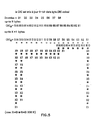
- the CRC N + 1 is updated after each reception of 9 bits of data by calculating the CRC on 16 bits by a cyclic permutation algorithm shown in fig. 5 on the values calculated X i from the data received D i and the values R i of the bits of the preceding CRC N according to the formula given in fig. 5.
- the information transmitted by this decoder (108R) is also transmitted on the one hand, to a state machine constituting a history buffer (1022 R ), and on the other hand, to a machine of state of the receiving port (1021 R ), and finally to an initialization state machine (1023 R ) of the port.
- the reception buffer management machine (101 R ) sends three signals (Connect, Outrdy, Status 0: 10), and receives the information on three lines as input (Istrr 0: 3).
- the signal (Outrdy) indicates that the output is ready, this signal indicates that there is a complete message awaiting reading.
- the Status signal indicates the status of the outputs: interruptions or not, indivisible operations or not, memory access / access registers, local / remote or ISCON / non ISCON, micro / displacement source (MOVER) - slaves (SLAVE), delayed responses where no, last message or not, data error or not, access out of memory or not, message insignificant or not.
- the Connect output indicates that the SLC port (10 0 ) is disconnected when this output is deactivated.
- the Istrr inputs allow the reception ports to be read in FIFO order, and the command which reads the last double word of a message generates the generation of a flow control character (token) associated with the buffer which becomes thus free.
- This flow control character is transmitted from the state machine for managing the reception buffers (101 R ) to the state machine for managing the transmission, and through the latter to the multiplexer (107). so as to transmit this information to the input port (10c) of the card (1c) associated in the serial link to the reception port (109 R ) from which the reception buffers (RDBUF) have just been read.
- the state machine for managing the transmission buffers (101 T ) has two Istatus and Istrw inputs, and an Inrdy output.
- This Inrdy output indicates that there is a free transmission buffer (TDBUF) waiting to be written.
- TBUF free transmission buffer
- the Istatus lines make it possible to specify the types of message to write, and to determine according to the value of the first two status bits the following meanings: 00 are not used, 01 it is only data, 10 it is is a header, 11 it is a header and data.
- the third bit Istatus indicates whether it is the last message or not.
- the fourth bit whether it is a data error or not; and the fifth bit if we have an external access to the memory or not.
- the signal Istrw makes it possible to write the buffers of transmissions (TDBUF) in FIFO order.
- the signal Istrw which writes the last double word of a message initializes the transmission of the message as soon as a remote reception buffer (RDBUF) (for example from port 10c) is declared free by a reception port (109 R ) connected to the serial link (120).
- RBUF remote reception buffer
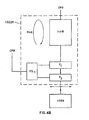
- the history buffer (I-HB) has 16 entries and contains either the last 16 characters which come from the serial link by the decoder (108R), or the last 16 control characters excluding the characters zero.
- writing to the history buffer can be inhibited by a specific command and the reading of the buffer is carried out thanks to a pointer (PHB) which allows a cyclic scanning of the buffer controlled by the microprocessor (11).
- the command of the history buffer is carried out by a register of commands (ICL1) (Fig. 4B) connected to the CPB command bus.
- the IHB history buffer is accessible to the microprocessor (11a, 11c) via the CPB control bus.
- the command register ICL1 is connected to 2 filters (F1, F2).
- the first F1 when activated by ICL1 does not leave pass that control characters, and when not enabled, is transparent.
- the second filter F2 lets pass all the characters not zero.
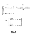
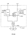
- the substitution state machine (1022 T ) (Fig. 4A) has a substitution buffer (I-sb) which has eight entries and its content is combined in an exclusive OR (10221) with the outgoing flow ( os, Out going stream) characters over a length of 7 characters.
- Substitution starts with the last character of a sequence activation.
- the read pointer PL of the substitution buffer (I-sb) addresses the first character of the buffer substitution (I-sb). This character which is null, by combining in the OR exclusive (10221) with the characters of the stream (o-s) does not modify these last, and the stream (o-s) is transmitted to the multiplexer (107).
- This I-tb buffer sends the activation sequence tc on an associated comparator (10222) which receives on its other inputs the outgoing flow (o-s).
- This start-up time is given when the activation sequence (tc) corresponds to the character stream outgoing (o-s).
- the output (10224) of the comparator activates the incrementer (10223) of the read pointer PL to allow simultaneous sending with each new character of the flow leaving a substitution character addressed among the 8 characters of the I-sb buffer by the read pointer.
- This activation buffer (I-tb) includes information (tv) who participates in the comparison and who indicates when it takes the value 00 that she doesn't use substitution. In case the information (tv) takes the value 10, the length of the activation sequence is equal to 1. When tv is 11, the length of the activation sequence is two characters. This substitution circuit is shown in FIG. 4A.
- a PE writing pointer accessible by the microprocessor (11a, 11c) through the CPB bus allows loading into the substitution buffer by the CPB bus the substitution characters.
- substitution circuit we manage to insert errors at the when desired, and by the circuit (CRC) to detect these errors. he is therefore possible by looping back the port on itself by the link (1090) and the Ict03 command, to detect correct operation of the error detection (CRC).
- CRC error detection
- the processor (11a) forces the port error injection mechanism (10a) and deliberately inserts a CRC control character into the message false. This character is transmitted by the port (10a) to the port (10c) of the circuit integrated (1c) slave and also coupled to a second processor (11c).
- This port (10c) detects a data error by calculating the message CRC receipt that does not correspond to the wrong CRC included by the mechanism insertion in the received message. This error detection generates the sending an interrupt message to the transmission circuit (1a), which is received by the processor (11a).
- This processor (11a) comes to read in the circuit of the second port (10c) the CRC value calculated on the transmitted data and deducted if the CRC circuit worked correctly by checking that the CRC value stored corresponds to the received CRC value.
- Error diagnosis is performed by reading the buffer history of occurrences that generate the interruption. This occurrence of errors also generates the interruption of the communication link to the processor so as to avoid the propagation of the error in the machine.
Landscapes
- Engineering & Computer Science (AREA)
- General Engineering & Computer Science (AREA)
- Theoretical Computer Science (AREA)
- Computer Hardware Design (AREA)
- Quality & Reliability (AREA)
- Physics & Mathematics (AREA)
- General Physics & Mathematics (AREA)
- Information Transfer Systems (AREA)
- Detection And Correction Of Errors (AREA)
- Test And Diagnosis Of Digital Computers (AREA)
Claims (16)
- Vorrichtung für die Erfassung von Fehlern mit integriertem Selbsttest auf einer integrierten Schaltung, die eine Funktion für Befehle für eine serielle Verbindung umfaßt, um einen Eingangs/Ausgangs-Port (100) für eine Kommunikation mit hohem Durchsatz zwischen einem parallelen Bus (L2CB, C2LB) und einer seriellen Verbindung zu bilden, wobei die integrierte Schaltung eine Ausgangs-Serialisierungsschaltung (109T) und eine Eingangs-Deserialisierungsschaltung (109R) umfaßt, dadurch gekennzeichnet, daß ein Einfügungspuffer (1022T, I-sb) an jedem ihrer Ausgänge mit einer Exklusiv-ODER-Funktion (10221) mit zwei Eingängen verbunden ist, wovon jeder zweite Eingang zu übertragende Informationen (o-s) empfängt, um mit Einfügungsinformationen, die vom Einfügungspufferspeicher stammen, Substitutionsinformationen zu bilden, wobei ein zusätzlicher Aktivierungspuffer (1022T, I-tb) den Vergleich der am Ausgang des Exklusiv-ODER gelieferten Folge mit einer in dem zusätzlichen Aktivierungspufferspeicher (I-tb) gespeicherten Folge ermöglicht, um das Aussenden der Substitutionsfolge zu validieren.
- Erfassungsvorrichtung nach Anspruch 1, dadurch gekennzeichnet, daß der zusätzliche Aktivierungspufferspeicher (I-tb) ein Gültigkeitsbit (tv) und die zu vergleichende Folge (tc) enthält.
- Erfassungsvorrichtung nach Anspruch 2, dadurch gekennzeichnet, daß die zu vergleichende Folge (tc) ein Null-Zeichen oder eine neutrale Nachricht (idle) sein kann.
- Vorrichtung nach Anspruch 2, dadurch gekennzeichnet, daß die zu vergleichende Folge (tc) entweder Steuerzeichen wie etwa die Rahmenanfänge (frame), die Rahmenenden, Jetons oder alle nicht neutralen Zeichen (non idle) umfassen kann.
- Vorrichtung nach einem der Ansprüche 1 bis 4, dadurch gekennzeichnet, daß der Port (100) eine serielle Verbindung (1090) umfaßt, die den Ausgang des Serialisierers (109T) zum Eingang des Deserialisierers (109R) zurückschleift, wobei die serielle Verbindung durch einen Rückschleifbefehlseingang, der von einem Steuerregister versorgt wird, validiert wird.
- Vorrichtung nach Anspruch 5, dadurch gekennzeichnet, daß der Port am Ausgang des Deserialisierers (109R) einen Historien-Pufferspeicher (1022) umfaßt, der entweder Steuerzeichen wie etwa die Rahmenanfänge (frame), die Rahmenenden, Jetons oder alle nicht neutralen Zeichen (non idle) speichert.
- Vorrichtung nach Anspruch 6, dadurch gekennzeichnet, daß die in dem Historienpufferspeicher (1022) gespeicherten Zeichen von der integrierten Schaltung verwendet werden, um die Ursache eines erfaßten Fehlers zu bestimmen oder um zu verifizieren, daß der Fehlererfassungsmechanismus in Betrieb ist.
- Vorrichtung nach einem der Ansprüche 1 bis 7, dadurch gekennzeichnet, daß der Port (109) wenigstens einen Pufferspeicher (TDBUF) für zu sendende Daten, die vom parallelen Bus stammen, oder einen Pufferspeicher (RDBUF) für zu empfangende Daten umfaßt und zwischen dem Eingangspufferspeicher (TDBUF) und der Ausgangsserialisiererschaltung oder zwischen dem Ausgangspufferspeicher (RDBUF) und der Eingangsdeserialisiererschaltung für den Sendeabschnitt eine Codeerzeugungsschaltung (CRC) bzw. für den Empfangsabschnitt eine Codesteuerschaltung (CRC) umfaßt.
- Vorrichtung nach Anspruch 5, dadurch gekennzeichnet, daß die Serialisiererschaltung und die Deserialisiererschaltung mit 1 Gigabaud, der Geschwindigkeit der seriellen Verbindung, arbeiten.
- Vorrichtung nach Anspruch 8, dadurch gekennzeichnet, daß die CRC-Erzeugungsschaltung unter Verwendung eines parallelen Algorithmes ein Wort mit 16 Bit liefert, um den CRC nach der Verschiebung, die der Steuerung eines Nonetts entspricht, zu berechnen.
- Vorrichtung nach Anspruch 8, dadurch gekennzeichnet, daß der Pufferspeicher (TDBUF) für Sendedaten oder der Pufferspeicher (RDBUF) für Empfangsdaten mit einem bestimmten Systemtakt arbeiten, der eine Frequenz besitzt, die jener des internen Busses der integrierten Schaltung entspricht.
- Vorrichtung nach einem der vorhergehenden Ansprüche, dadurch gekennzeichnet, daß eine 9/12-Codierungsschaltung für serielles Senden mit dem Serialisierer (109T) gekoppelt ist und daß eine 9/12-Decodierungsschaltung für den Empfang mit dem Deserialisierer (109R) gekoppelt ist, um ein normales Zeichen aus neun Bit und ein Steuerzeichen im Code mit 12 Bit zu transformieren, was beim Empfang eine Extraktion des Taktsignals und einer kontinuierlichen Null-Komponente beim Senden ermöglicht.
- Verfahren für die Erfassung von Fehlern, das an einem Seriell-Parallel-Kommunikationsport mit hohem Durchsatz die Vorrichtung nach Anspruch 1 verwendet und ferner eine Schaltung für die Erzeugung von Steuerzeichen CRC mit zyklischer Redundanz, die einen Fehlereinleitungsmechanismus enthält, verwendet, dadurch gekennzeichnet, daß es umfaßt:einen Schritt bei, dem zu sendende Informationen an den Port geschickt werden;einen Schritt, bei dem die CRC der zu sendenden Informationen berechnet und die CRC, die den zu sendenden Informationen entsprechen, gespeichert werden;einen Schritt, bei dem Informationen, die durch Validierung des Fehlereinleitungsmechanismus fehlerhaft gemacht werden, erzeugt werden, und einen Schritt, bei dem die fehlerhaft gemachten Informationen zu einer integrierten Schaltung, die mit demselben Port-Typ ausgerüstet ist, gesendet werden;einen Schritt, bei dem Datenfehler von der CRC-Steuerschaltung des Empfangs-Ports erfaßt werden;einen Schritt, bei dem eine Unterbrechungsnachricht zur integrierten Schaltung des Sende-Ports gesendet wird;einen Schritt, bei dem durch einen mit dem parallelen Bus des Sende-Ports verbundenen Mikroprozessors der von der CRC-Schaltung des Empfangs-Ports berechnete Wert gelesen wird; undeinen Schritt, bei dem der gespeicherte Wert mit dem gelesenen Wert verglichen wird.
- Fehlererfassungsverfahren nach Anspruch 13, dadurch gekennzeichnet, daß das Verfahren einen Schritt umfaßt, bei dem die Sende-Serialisiererschaltung (109T) zur Empfangs-Deserialisiererschaltung (109R) desselben Ports der integrierten Schaltung zurückgeschleift wird.
- Verfahren nach Anspruch 13, dadurch gekennzeichnet, daß der Fehlereinleitungsmechanismus umfaßt:einen Schritt, bei dem Einleitungsinformationen, die mit den gesendeten Informationen zu kombinieren sind, um den Fehler zu erzeugen, in dem Einfügungspuffer (I-sb) gespeichert werden;einen Schritt, bei dem der Aktivierungspuffer (I-tb) des Einleitungsmechanismus, der eine Folge aus einem oder aus zwei Zeichen enthält, geladen wird;einen Schritt, bei dem Substitutionsinformationen, die sich aus der Kombination der gesendeten Informationen mit den eingeleiteten Informationen ergeben, substituiert werden, sobald die kombinierten Informationen jenen des Aktivierungspuffers (I-tb) entsprechen.
- Verfahren nach Anspruch 15, dadurch gekennzeichnet, daß die Länge der Substitutionsfolge auf 8 Zeichen begrenzt ist.
Applications Claiming Priority (2)
| Application Number | Priority Date | Filing Date | Title |
|---|---|---|---|
| FR9701944 | 1997-02-19 | ||
| FR9701944A FR2759796B1 (fr) | 1997-02-19 | 1997-02-19 | Dispositif et procede de detection d'erreurs sur un circuit integre comportant un port parallele serie |
Publications (2)
| Publication Number | Publication Date |
|---|---|
| EP0860778A1 EP0860778A1 (de) | 1998-08-26 |
| EP0860778B1 true EP0860778B1 (de) | 2003-05-14 |
Family
ID=9503904
Family Applications (1)
| Application Number | Title | Priority Date | Filing Date |
|---|---|---|---|
| EP98400331A Expired - Lifetime EP0860778B1 (de) | 1997-02-19 | 1998-02-12 | Vorrichtung und Verfahren zur Fehlererkennung in einer integrierten Schaltung mit einer parallelen-seriellen Anschlussstelle |
Country Status (5)
| Country | Link |
|---|---|
| US (1) | US6173423B1 (de) |
| EP (1) | EP0860778B1 (de) |
| JP (1) | JP2988901B2 (de) |
| DE (1) | DE69814491T2 (de) |
| FR (1) | FR2759796B1 (de) |
Families Citing this family (26)
| Publication number | Priority date | Publication date | Assignee | Title |
|---|---|---|---|---|
| US6560290B2 (en) * | 1998-01-20 | 2003-05-06 | Silicon Image, Inc. | CMOS driver and on-chip termination for gigabaud speed data communication |
| US7167892B2 (en) * | 1998-03-19 | 2007-01-23 | Isochron, Inc. | System, method and apparatus for vending machine wireless audit and cashless transaction transport |
| US6385236B1 (en) * | 1998-10-05 | 2002-05-07 | Lsi Logic Corporation | Method and Circuit for testing devices with serial data links |
| US6886126B1 (en) * | 2000-03-23 | 2005-04-26 | Cypress Semiconductor Corp. | Apparatus and protocol for detected error propagation in serial-transport block-coded interfaces |
| US7016430B1 (en) | 2001-03-21 | 2006-03-21 | Cyrpess Semiconductor Corp. | Apparatus and protocol for exception propagation in serial transport block coded interfaces |
| US20030165242A1 (en) * | 2001-11-19 | 2003-09-04 | Adrian Walker | Confusion encryption |
| US8185812B2 (en) * | 2003-03-20 | 2012-05-22 | Arm Limited | Single event upset error detection within an integrated circuit |
| DE602004001869T2 (de) * | 2003-03-20 | 2007-05-03 | Arm Ltd., Cherry Hinton | Fehlererkennung und fehlerbehebung für systematische und zufällige fehler innerhalb einer verarbeitungsstufe einer integrierten schaltung |
| US7278080B2 (en) * | 2003-03-20 | 2007-10-02 | Arm Limited | Error detection and recovery within processing stages of an integrated circuit |
| US7260001B2 (en) * | 2003-03-20 | 2007-08-21 | Arm Limited | Memory system having fast and slow data reading mechanisms |
| US8650470B2 (en) | 2003-03-20 | 2014-02-11 | Arm Limited | Error recovery within integrated circuit |
| US8234399B2 (en) * | 2003-05-29 | 2012-07-31 | Seagate Technology Llc | Method and apparatus for automatic phy calibration based on negotiated link speed |
| US7725892B2 (en) | 2003-07-01 | 2010-05-25 | Hewlett-Packard Development Company, L.P. | Field-replaceable unit revision compatibility |
| US7730476B2 (en) | 2003-07-01 | 2010-06-01 | Hewlett-Packard Development Company, L.P. | Field-replaceable unit revision compatibility |
| US7606253B2 (en) * | 2004-01-12 | 2009-10-20 | Hewlett-Packard Development Company, L.P. | Successful transactions |
| US7613958B2 (en) | 2004-01-12 | 2009-11-03 | Hewlett-Packard Development Company, L.P. | Error detection in a system having coupled channels |
| US7672222B2 (en) * | 2004-01-12 | 2010-03-02 | Hewlett-Packard Development Company, L.P. | Link failures |
| US7624213B2 (en) * | 2005-02-11 | 2009-11-24 | Hewlett-Packard Development Company, L.P. | Passing identification information |
| FR2870958B1 (fr) * | 2004-05-25 | 2008-01-25 | Hewlett Packard Development Co | Systeme pour injecter des erreurs dans une liaison de commun ications |
| US20060184707A1 (en) * | 2005-02-11 | 2006-08-17 | Lesartre Gregg B | Error injection |
| US7721159B2 (en) * | 2005-02-11 | 2010-05-18 | Hewlett-Packard Development Company, L.P. | Passing debug information |
| US8073042B1 (en) | 2005-04-13 | 2011-12-06 | Cypress Semiconductor Corporation | Recursive range controller |
| US8171386B2 (en) * | 2008-03-27 | 2012-05-01 | Arm Limited | Single event upset error detection within sequential storage circuitry of an integrated circuit |
| US8161367B2 (en) * | 2008-10-07 | 2012-04-17 | Arm Limited | Correction of single event upset error within sequential storage circuitry of an integrated circuit |
| US8493120B2 (en) | 2011-03-10 | 2013-07-23 | Arm Limited | Storage circuitry and method with increased resilience to single event upsets |
| US9262270B2 (en) * | 2012-12-28 | 2016-02-16 | Intel Corporation | Live error recovery |
Family Cites Families (12)
| Publication number | Priority date | Publication date | Assignee | Title |
|---|---|---|---|---|
| GB2097653B (en) | 1981-04-07 | 1985-06-05 | Sadler James & Sons Ltd | Insulated containers for dispensing liquids |
| JPS59136843A (ja) * | 1983-01-27 | 1984-08-06 | Yokogawa Hokushin Electric Corp | シリアルデ−タ転送における誤り訂正機能の動作チエツク方法 |
| JPS6159547A (ja) * | 1984-08-30 | 1986-03-27 | Yokogawa Hokushin Electric Corp | 誤り訂正機能の動作チエツク装置 |
| US4712215A (en) * | 1985-12-02 | 1987-12-08 | Advanced Micro Devices, Inc. | CRC calculation machine for separate calculation of checkbits for the header packet and data packet |
| US4809273A (en) * | 1987-01-29 | 1989-02-28 | International Business Machines Corporation | Device for verifying operation of a checking code generator |
| US4935925A (en) * | 1987-03-11 | 1990-06-19 | Aristacom International, Inc. | Adaptive digital network interface |
| US4907225A (en) * | 1987-04-03 | 1990-03-06 | Advanced Micro Devices, Inc. | Data protocol controller |
| US4827477A (en) * | 1987-05-15 | 1989-05-02 | Grumman Aerospace Corporation | Bus interface unit |
| US5394390A (en) * | 1993-10-29 | 1995-02-28 | International Business Machines Corporation | FDDI network test adapter history store circuit (HSC) |
| US5754525A (en) * | 1994-12-30 | 1998-05-19 | Advanced Micro Devices Inc. | Programmable delay of disrupt for secure networks |
| US5581559A (en) * | 1995-03-17 | 1996-12-03 | Advanced Micro Devices, Inc. | Inverse packet disrupt for secure networks |
| US5907566A (en) * | 1997-05-29 | 1999-05-25 | 3Com Corporation | Continuous byte-stream encoder/decoder using frequency increase and cyclic redundancy check |
-
1997
- 1997-02-19 FR FR9701944A patent/FR2759796B1/fr not_active Expired - Fee Related
-
1998
- 1998-02-09 US US09/020,671 patent/US6173423B1/en not_active Expired - Lifetime
- 1998-02-12 DE DE69814491T patent/DE69814491T2/de not_active Expired - Lifetime
- 1998-02-12 EP EP98400331A patent/EP0860778B1/de not_active Expired - Lifetime
- 1998-02-19 JP JP10037111A patent/JP2988901B2/ja not_active Expired - Fee Related
Also Published As
| Publication number | Publication date |
|---|---|
| US6173423B1 (en) | 2001-01-09 |
| EP0860778A1 (de) | 1998-08-26 |
| DE69814491D1 (de) | 2003-06-18 |
| FR2759796B1 (fr) | 2001-12-07 |
| JP2988901B2 (ja) | 1999-12-13 |
| DE69814491T2 (de) | 2004-04-08 |
| FR2759796A1 (fr) | 1998-08-21 |
| JPH10260914A (ja) | 1998-09-29 |
Similar Documents
| Publication | Publication Date | Title |
|---|---|---|
| EP0860778B1 (de) | Vorrichtung und Verfahren zur Fehlererkennung in einer integrierten Schaltung mit einer parallelen-seriellen Anschlussstelle | |
| EP0094179B1 (de) | AnschluB für Rechnerverbindung | |
| EP0003493B1 (de) | Datenübertragungssystem zwischen Stationen die in einer Schleife miteinander verbunden sind | |
| EP0349371B1 (de) | Rechneranlage mit einer zentralen Zwischenverbindung | |
| EP0272969B1 (de) | Verfahren und programmierbare Vorrichtung zur Umkodierung von Zeichenketten | |
| EP0159941A2 (de) | Serieller Verbindungsbus für Datenverabeitungssystem und Verfahren zum Informationsaustausch | |
| FR2637997A1 (fr) | Procede et dispositif pour mettre en file d'attente des requetes et des reponses sur un bus | |
| FR2479534A1 (fr) | Circuit de detection d'erreur pour une memoire | |
| US6202108B1 (en) | Process and system for initializing a serial link between two integrated circuits comprising a parallel-serial port using two clocks with different frequencies | |
| FR2737029A1 (fr) | Dispositif d'interface entre un calculateur a architecture redondante et un moyen de communication | |
| US20220398177A1 (en) | Error rate measuring apparatus and error rate measuring method | |
| EP0048781A1 (de) | Leitungssteuerung für einen Vorschaltrechner in einem Datennetz | |
| US6141350A (en) | Auto-negotiation using negative link pulses | |
| EP0120495B1 (de) | Einrichtung zum Austausch von kodierten Nachrichten zwischen Stationen | |
| EP0102434A1 (de) | Anordnung zur Meldung an die zentrale Steuereinheit einer Datenverarbeitungsanlage von Fehlern, die sich in Adaptern ereignen | |
| FR2765425A1 (fr) | Procede de detection d'erreurs sur une liaison serie d'un circuit integre et dispositif de mise en oeuvre du procede | |
| US6862283B2 (en) | Method and apparatus for maintaining packet ordering with error recovery among multiple outstanding packets between two devices | |
| US4555774A (en) | Fast response for switched data networks | |
| EP0860782B1 (de) | Initialisierungsverfahren einer seriellen Verbindung zwischen zwei integrierten Schaltungen mit einer parallelen zu seriellen Schnittstelle und Anordnung zur Durchführung des Verfahrens | |
| EP0974902B1 (de) | Verfahren um Fehler auf einer seriellen Verbindung einer integrierten Schaltung zu erkennen und Vorrichtung zur Durchführung des Verfahrens | |
| KR0174853B1 (ko) | 상대방 메모리를 이용한 두 프로세서간 비동기 직렬 통신 송/수신 장치 | |
| US7362739B2 (en) | Methods and apparatuses for detecting clock failure and establishing an alternate clock lane | |
| EP1560372A1 (de) | Verfahren und Vorrichtung zur automatischen Erkennung der Bitrate von CAN-Bus-Netzwerk | |
| EP0190060B1 (de) | Verfahren und Vorrichtung zur sicheren Nachrichtenrundsendung in einem Ringnetz | |
| EP0895159B1 (de) | Verfahren zur Entleeren von Hochdurchsatzübertragungspuffern und Vorrichtung zur Ausführung des Verfahrens |
Legal Events
| Date | Code | Title | Description |
|---|---|---|---|
| PUAI | Public reference made under article 153(3) epc to a published international application that has entered the european phase |
Free format text: ORIGINAL CODE: 0009012 |
|
| AK | Designated contracting states |
Kind code of ref document: A1 Designated state(s): DE FR GB IT |
|
| AX | Request for extension of the european patent |
Free format text: AL;LT;LV;MK;RO;SI |
|
| 17P | Request for examination filed |
Effective date: 19990226 |
|
| AKX | Designation fees paid |
Free format text: DE FR GB IT |
|
| RBV | Designated contracting states (corrected) |
Designated state(s): DE FR GB IT |
|
| GRAH | Despatch of communication of intention to grant a patent |
Free format text: ORIGINAL CODE: EPIDOS IGRA |
|
| RIC1 | Information provided on ipc code assigned before grant |
Free format text: 7G 06F 11/267 A |
|
| GRAH | Despatch of communication of intention to grant a patent |
Free format text: ORIGINAL CODE: EPIDOS IGRA |
|
| GRAA | (expected) grant |
Free format text: ORIGINAL CODE: 0009210 |
|
| RTI1 | Title (correction) |
Free format text: DEVICE AND METHOD FOR ERROR DETECTION IN AN INTEGRATED CIRCUIT WITH A PARALLEL-SERIAL PORT |
|
| AK | Designated contracting states |
Designated state(s): DE FR GB IT |
|
| REG | Reference to a national code |
Ref country code: GB Ref legal event code: FG4D Free format text: NOT ENGLISH |
|
| GBT | Gb: translation of ep patent filed (gb section 77(6)(a)/1977) |
Effective date: 20030515 |
|
| REF | Corresponds to: |
Ref document number: 69814491 Country of ref document: DE Date of ref document: 20030618 Kind code of ref document: P |
|
| PLBE | No opposition filed within time limit |
Free format text: ORIGINAL CODE: 0009261 |
|
| STAA | Information on the status of an ep patent application or granted ep patent |
Free format text: STATUS: NO OPPOSITION FILED WITHIN TIME LIMIT |
|
| 26N | No opposition filed |
Effective date: 20040217 |
|
| REG | Reference to a national code |
Ref country code: FR Ref legal event code: PLFP Year of fee payment: 18 |
|
| PGFP | Annual fee paid to national office [announced via postgrant information from national office to epo] |
Ref country code: DE Payment date: 20150623 Year of fee payment: 18 Ref country code: GB Payment date: 20150626 Year of fee payment: 18 |
|
| PGFP | Annual fee paid to national office [announced via postgrant information from national office to epo] |
Ref country code: FR Payment date: 20150625 Year of fee payment: 18 |
|
| PGFP | Annual fee paid to national office [announced via postgrant information from national office to epo] |
Ref country code: IT Payment date: 20150624 Year of fee payment: 18 |
|
| REG | Reference to a national code |
Ref country code: DE Ref legal event code: R119 Ref document number: 69814491 Country of ref document: DE |
|
| GBPC | Gb: european patent ceased through non-payment of renewal fee |
Effective date: 20160212 |
|
| REG | Reference to a national code |
Ref country code: FR Ref legal event code: ST Effective date: 20161028 |
|
| PG25 | Lapsed in a contracting state [announced via postgrant information from national office to epo] |
Ref country code: IT Free format text: LAPSE BECAUSE OF NON-PAYMENT OF DUE FEES Effective date: 20160212 |
|
| PG25 | Lapsed in a contracting state [announced via postgrant information from national office to epo] |
Ref country code: DE Free format text: LAPSE BECAUSE OF NON-PAYMENT OF DUE FEES Effective date: 20160901 Ref country code: GB Free format text: LAPSE BECAUSE OF NON-PAYMENT OF DUE FEES Effective date: 20160212 Ref country code: FR Free format text: LAPSE BECAUSE OF NON-PAYMENT OF DUE FEES Effective date: 20160229 |