EP0860879A2 - Interconnexion multicouche d'un dispositif semi-conducteur et son procédé de fabrication - Google Patents
Interconnexion multicouche d'un dispositif semi-conducteur et son procédé de fabrication Download PDFInfo
- Publication number
- EP0860879A2 EP0860879A2 EP98102926A EP98102926A EP0860879A2 EP 0860879 A2 EP0860879 A2 EP 0860879A2 EP 98102926 A EP98102926 A EP 98102926A EP 98102926 A EP98102926 A EP 98102926A EP 0860879 A2 EP0860879 A2 EP 0860879A2
- Authority
- EP
- European Patent Office
- Prior art keywords
- film
- insulator
- level interconnections
- level
- interconnections
- Prior art date
- Legal status (The legal status is an assumption and is not a legal conclusion. Google has not performed a legal analysis and makes no representation as to the accuracy of the status listed.)
- Withdrawn
Links
Images


Classifications
-
- H—ELECTRICITY
- H10—SEMICONDUCTOR DEVICES; ELECTRIC SOLID-STATE DEVICES NOT OTHERWISE PROVIDED FOR
- H10W—GENERIC PACKAGES, INTERCONNECTIONS, CONNECTORS OR OTHER CONSTRUCTIONAL DETAILS OF DEVICES COVERED BY CLASS H10
- H10W20/00—Interconnections in chips, wafers or substrates
- H10W20/01—Manufacture or treatment
- H10W20/071—Manufacture or treatment of dielectric parts thereof
- H10W20/072—Manufacture or treatment of dielectric parts thereof of dielectric parts comprising air gaps
-
- H—ELECTRICITY
- H10—SEMICONDUCTOR DEVICES; ELECTRIC SOLID-STATE DEVICES NOT OTHERWISE PROVIDED FOR
- H10W—GENERIC PACKAGES, INTERCONNECTIONS, CONNECTORS OR OTHER CONSTRUCTIONAL DETAILS OF DEVICES COVERED BY CLASS H10
- H10W20/00—Interconnections in chips, wafers or substrates
- H10W20/40—Interconnections external to wafers or substrates, e.g. back-end-of-line [BEOL] metallisations or vias connecting to gate electrodes
- H10W20/45—Interconnections external to wafers or substrates, e.g. back-end-of-line [BEOL] metallisations or vias connecting to gate electrodes characterised by their insulating parts
- H10W20/46—Interconnections external to wafers or substrates, e.g. back-end-of-line [BEOL] metallisations or vias connecting to gate electrodes characterised by their insulating parts comprising air gaps
-
- H—ELECTRICITY
- H10—SEMICONDUCTOR DEVICES; ELECTRIC SOLID-STATE DEVICES NOT OTHERWISE PROVIDED FOR
- H10W—GENERIC PACKAGES, INTERCONNECTIONS, CONNECTORS OR OTHER CONSTRUCTIONAL DETAILS OF DEVICES COVERED BY CLASS H10
- H10W20/00—Interconnections in chips, wafers or substrates
- H10W20/40—Interconnections external to wafers or substrates, e.g. back-end-of-line [BEOL] metallisations or vias connecting to gate electrodes
- H10W20/45—Interconnections external to wafers or substrates, e.g. back-end-of-line [BEOL] metallisations or vias connecting to gate electrodes characterised by their insulating parts
- H10W20/48—Insulating materials thereof
-
- H—ELECTRICITY
- H10—SEMICONDUCTOR DEVICES; ELECTRIC SOLID-STATE DEVICES NOT OTHERWISE PROVIDED FOR
- H10W—GENERIC PACKAGES, INTERCONNECTIONS, CONNECTORS OR OTHER CONSTRUCTIONAL DETAILS OF DEVICES COVERED BY CLASS H10
- H10W20/00—Interconnections in chips, wafers or substrates
- H10W20/40—Interconnections external to wafers or substrates, e.g. back-end-of-line [BEOL] metallisations or vias connecting to gate electrodes
- H10W20/495—Capacitive arrangements or effects of, or between wiring layers
-
- H—ELECTRICITY
- H10—SEMICONDUCTOR DEVICES; ELECTRIC SOLID-STATE DEVICES NOT OTHERWISE PROVIDED FOR
- H10W—GENERIC PACKAGES, INTERCONNECTIONS, CONNECTORS OR OTHER CONSTRUCTIONAL DETAILS OF DEVICES COVERED BY CLASS H10
- H10W20/00—Interconnections in chips, wafers or substrates
- H10W20/01—Manufacture or treatment
- H10W20/071—Manufacture or treatment of dielectric parts thereof
- H10W20/098—Manufacture or treatment of dielectric parts thereof by filling between adjacent conductive parts
Definitions
- the present invention relates to a semiconductor device and a method for manufacturing the same, and more specifically to a multilevel interconnection in a semiconductor device and a method for forming the same.
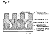
- Reference Numeral 1 designates a substrate
- Reference Numeral 2 indicates an insulator layer formed on the substrate 1.
- Reference Numeral 3 shows lower level interconnections 3 formed on the insulator layer 2
- Reference Numerals 4a and 4b denote insulator films formed to cover the lower level interconnections 3.
- Reference Numeral 5 designates a cavity formed between adjacent lower level interconnection 3
- Reference Numeral 6 indicates a metal pillar extending through the insulator films 4a and 4b to contact with a target one of the lower level interconnection 3.
- Reference Numeral 7 shows upper level interconnections formed on the insulator film 4b, and one of the upper level interconnections 7 is connected to the metal pillar 7.
- Reference Numeral 8 denotes an organic film 8
- Reference Numeral 10 designates a hollow formed in the metal pillar 7.
- the metal pillar 6 for electrically connecting the upper level interconnection 7 and the lower level interconnection 3 has often become formed to deviate from the lower level interconnection 3, so that a portion of the metal pillar 6 extends into a region between two adjacent lower level interconnections 3.
- the metal pillar 6 reaches the cavity 5 in a deviated portion of the metal pillar 6, so that a gas retained in the cavity 5 is discharged to create the hollow 10 in the metal pillar 6.
- the metal pillar 5 is formed to fill up the cavity 5 between the lower level interconnections 3, which results in an increased leak current between the lower level interconnections 3.
- the metal pillar 6 contacts with the organic film 8 in a deviated portion of the metal pillar 6, so that because of a degasification of the organic film 8, the hollow 10 is formed in the metal pillar 6. Similarly, this results in an increased resistance of a connection resistance and in a lowered reliability.
- Another object of the present invention is to provide a multilevel interconnection in a semiconductor device in which a metal pillar for connecting interconnections of different levels is stably formed by forming between adjacent interconnections of the same level, an insulator having a lower dielectric constant, such as a cavity and an organic film having a lower dielectric constant, other than a silicon oxide film, and by forming the metal pillar in no contact with the insulator having the lower dielectric constant.
- Still another object of the present invention is to provide a method for forming the above mentioned multilevel interconnection in the semiconductor device.
- a semiconductor device including first level interconnections and second level interconnections separated from each other by an interlayer insulator film, and a connection member for electrically connecting one of the first level interconnections and one of the second level interconnections to each other, wherein a capacitance reducing insulator is formed between adjacent first level interconnections to reduce a line-to-line capacitance in the first level interconnections, and a separation film is formed to surround the capacitance reducing insulator so as to isolate the connection member from the capacitance reducing insulator film.
- the capacitance reducing insulator can be formed of air, an insulating gas, an insulating liquid, an insulating organic material, an insulating inorganic material excluding a silicon oxide, or a porous insulator.
- a method for forming a semiconductor device including first level interconnections and second level interconnections separated from each other by an interlayer insulator film, and a connection member for electrically connecting one of the first level interconnections and one of the second level interconnections to each other, the method including:
- the capacitance reducing step is achieved by growing the separation film between the first level interconnections on the insulator layer by means of a plasma chemical vapor deposition process applying a high frequency electric field, so that, as the capacitance reducing insulator, a cavity is simultaneously created in the separation film between adjacent first level interconnections.
- the interlayer insulator film forming step is achieved by forming a silicon oxide film as the interlayer insulator film by means of a plasma chemical vapor deposition process applying a high frequency electric field.
- connection member for connecting one of the first level interconnections to one of the second level interconnections is surrounded by the silicon oxide. Therefore, the connection member is not subjected to any influence of the insulator material other than the silicon oxide.
- a portion of an insulating film for insulating the first level interconnections from one another and from the second level interconnections is formed of an insulator material other than the silicon oxide, and the insulator material other than the silicon oxide is selectively removed from a location where the connection member for connecting one of the first level interconnections to one of the second level interconnections is to be formed.
- a silicon oxide is filled into the selectively removed portion of the insulator material other than the silicon oxide, and the connection member for connecting the one first level interconnection to the one second level interconnection is formed to penetrate through the silicon oxide to reach the one first level interconnection, with the result that the connection member for connecting the one first level interconnection to the one second level interconnection is surrounded by the silicon oxide. Since the second insulator film is formed of the silicon oxide having a high reliability, a stable connection can be obtained.
- FIG. 2 there is shown a diagrammatic sectional view of an embodiment of the multilevel interconnection structure in the semiconductor device in accordance with the present invention.
- the shown embodiment includes, as fundamental constituents, first level interconnections 3, capacitance reducing insulators 5, a separation film 4a, an interlayer insulator film 4b, second level interconnections 7, and a vertical connection member 6.
- the first level interconnections 3 are formed in a given pattern on an insulator layer 2 formed on a substrate 1.
- the capacitance reducing insulators 5 are formed between adjacent first level interconnections 3 and 3 on the insulator layer 2, for the purpose of reducing the line-to-line capacitance of the first level interconnections 3.
- the capacitance reducing insulators 5 are formed of a cavity, but is not limited to only the cavity.
- the capacitance reducing insulators 5 can be formed of an insulating gas, an insulating liquid, an insulating organic material, an insulating inorganic material excluding a silicon oxide, or a porous insulator, or a stacked or layered matter of two or more of these materials.
- the separation film 4a surrounds the capacitance reducing insulators 5 for preventing the capacitance reducing insulators 5 from being contacted with the vertical connection member 6.
- the interlayer insulator film 4b is formed to cover all the surface for insulating between the first level interconnections and the second level interconnections 7.
- the second level interconnections 7 are formed in a given pattern on an upper planarized surface of the interlayer insulator film 4b, and one of the second level interconnections 7 is electrically connected through the vertical connection member 6 to one of the first level interconnections 3.
- the insulator layer 2 is preferably formed of an silicon oxide film, a BPSG (borophosphosilicate glass) film, a PSG (phosphosilicate glass) film, a silicon nitride film, or a stacked or layered structure of two or more of these materials.
- the first level interconnections 3 and the second level interconnections 6 are preferably formed of polysilicon, a metal silicide, aluminum or alloy thereof, copper or alloy thereof, silver or alloy thereof, or a refractory metal such as tungsten.
- the separation film 4a and the interlayer insulator film 4b are preferably formed of silicon oxide, fluorine-added silicon oxide or silicon oxynitride film.
- the one first level interconnection 3 and the one second level interconnection 7 are electrically connected to each other by a metal pillar formed as the vertical connection member 6.
- the metal pillar 6 since there is a limitation in a photolithography, the metal pillar 6 is often formed to partially deviate from the upper surface of the one first level interconnection 3, and the portion of the metal pillar 6 deviated from the upper surface of the one first level interconnection 3 extends into a region between the adjacent first level interconnections 3, as mentioned hereinbefore.
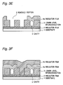
- lower level interconnections 3 are formed in a given pattern on the insulator layer 2 formed on the substrate 1, and then, as shown in Fig. 3B, as the separation film, a silicon oxide film 4a is formed to cover the lower level interconnections 3 and the insulator layer 2, by means of a biased ECR-CVD (electron cyclotron resonance plasma CVD) process which is one kind of a plasma CVD process applying a high frequency electric field onto the substrate.
- ECR-CVD electron cyclotron resonance plasma CVD
- a microwave introducing port 14 is provided above a plasma chamber 13 so that a microwave is introduced through this port 14 into the plasma chamber 13.
- the plasma chamber 13 includes gas supplying ports 11a and 11b and an exhausting port 15, so that reaction gases are supplied through the gas supplying ports 11a and 11b into the plasma chamber 13, and unnecessary gases are exhausted through the exhausting port 15 from the plasma chamber 13.
- a susceptor 12 is provided in the plasma chamber 13.
- a substrate 1, which is a workpiece, is located on the susceptor 12.
- This susceptor 12 is connected to a high frequency power supply 16 for a RF biasing.
- a main coil 17 and an auxiliary coil 18 are provided as shown to generate a magnetic field.
- An example of the specific film deposition condition is that the flow rate of the silane is 50 sccm, the flow rate of oxygen is 75 sccm, the flow rate of argon is 70 sccm, the microwave power is 2000 W, the RF biasing power is 1400 W and the film deposition temperature is about 350°C.
- the cavity 5 is formed as the capacitance reducing insulator, as shown in Fig. 3B.
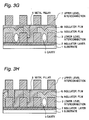
- the silicon oxide film 4a is removed from a tolerable region covering the extent in which a hole for the metal pillar 6 formed by a photolithography and a dry etching is allowed to deviate from a target lower level interconnection 3 to be contacted with the possible metal pillar. Namely, a removed portion 9 is formed in the silicon oxide film 4a. At this time, when two or more metal pillars 6 are to be formed adjacent to each other, the removed portion 4 is formed to extend over a continuous tolerable region covering a plurality of metal pillar formation positions, as shown in Fig. 3E.
- the silicon oxide film 4a when the silicon oxide film 4a is selectively removed by the dry etching, the silicon oxide film 4a in contact with the target lower level interconnection 3 in the above mentioned tolerable region in which the hole for the metal pillar 6 is allowed to deviate from the target lower level interconnection 3, is not completely removed, but can be rather partially left to form a side wall covering the lower level interconnection 3, as shown in Fig. 3D.
- a silicon oxide film 4b is deposited to fill up the removed portion 9 and to cover the insulator film 4a, also by the biased ECR-CVD process.
- an example of the specific film deposition condition is that the flow rate of the silane is 30 sccm, the flow rate of oxygen is 45 sccm, the flow rate of argon is 70 sccm, the microwave power is 2000 W, the RF biasing power is 1400 W and the film deposition temperature is about 350°C.
- an upper surface of the silicon oxide film 4b is planarized by for example a CMP (chemical mechanical polishing) process, and a hole for the metal pillar 6 is formed to penetrate through the insulator film 4b filled in the removed portion, to reach the target lower level interconnection 3, and then, the hole is filled with a metal, so that the metal pillar 6 is formed in contact with the target lower level interconnection 3, as shown in Fig. 3G.
- upper level interconnections 7 are formed in a given pattern on the upper surface of the silicon oxide film 4b, as shown in Fig. 3G.
- the removed portion 4 is formed to extend over a plurality of metal pillar formation positions as shown in Fig. 3E, two or more metal pillars 6 are formed to penetrate through the insulator film 4b so as to contact with two or more adjacent lower level interconnections as shown in Fig. 3H.
- the metal pillar 6 and the cavity 5 can be prevented from being contacted to each other.
- interconnections for example, metal interconnections, of different levels, with high stability and high reliability.
- the embodiment shown in Figs. 3A to 3H has two levels of metal interconnection.
- the present invention can be applied to a multilevel interconnection structure including three or more levels of metal interconnection.
- the capacitance reducing insulator formed between adjacent interconnections of the same level has been constituted of cavity, but can be formed of an organic insulator film having a lower dielectric constant, a porous silicon oxide film or a fluorine-added silicon oxide. This would also be a matter of course to persons skilled in the art.
- the capacitance reducing insulator formed between adjacent interconnections is completely surrounded by the separation film, so that the capacitance reducing insulator is maintained to be never contacted with the vertical connection member, with the result that the vertical connection member is protected from the adverse affect of the capacitance reducing insulator. Accordingly, the interconnections of different levels can be surely connected to each other through the vertical connection member, and the vertical connection having a reduced resistance can be formed.
Landscapes
- Internal Circuitry In Semiconductor Integrated Circuit Devices (AREA)
- Electrodes Of Semiconductors (AREA)
- Local Oxidation Of Silicon (AREA)
Applications Claiming Priority (3)
| Application Number | Priority Date | Filing Date | Title |
|---|---|---|---|
| JP36424/97 | 1997-02-20 | ||
| JP3642497 | 1997-02-20 | ||
| JP09036424A JP3085231B2 (ja) | 1997-02-20 | 1997-02-20 | 半導体装置の製造方法 |
Publications (2)
| Publication Number | Publication Date |
|---|---|
| EP0860879A2 true EP0860879A2 (fr) | 1998-08-26 |
| EP0860879A3 EP0860879A3 (fr) | 2000-05-24 |
Family
ID=12469454
Family Applications (1)
| Application Number | Title | Priority Date | Filing Date |
|---|---|---|---|
| EP98102926A Withdrawn EP0860879A3 (fr) | 1997-02-20 | 1998-02-19 | Interconnexion multicouche d'un dispositif semi-conducteur et son procédé de fabrication |
Country Status (4)
| Country | Link |
|---|---|
| US (2) | US5861674A (fr) |
| EP (1) | EP0860879A3 (fr) |
| JP (1) | JP3085231B2 (fr) |
| KR (1) | KR100262917B1 (fr) |
Cited By (3)
| Publication number | Priority date | Publication date | Assignee | Title |
|---|---|---|---|---|
| WO2000044044A1 (fr) * | 1999-01-20 | 2000-07-27 | Koninklijke Philips Electronics N.V. | Procede de reduction de la capacitance entre des interconnexions en formant des vides dans le materiau dielectrique |
| EP1146567A1 (fr) * | 2000-04-14 | 2001-10-17 | Infineon Technologies AG | Diode et procédé pour sa fabrication |
| RU2459313C1 (ru) * | 2011-03-21 | 2012-08-20 | Открытое акционерное общество "НИИ молекулярной электроники и завод "Микрон" | Способ изготовления многоуровневой металлизации интегральных микросхем с пористым диэлектрическим слоем в зазорах между проводниками |
Families Citing this family (28)
| Publication number | Priority date | Publication date | Assignee | Title |
|---|---|---|---|---|
| JP2914282B2 (ja) * | 1996-03-25 | 1999-06-28 | 日本電気株式会社 | 半導体装置の製造方法 |
| TW571373B (en) * | 1996-12-04 | 2004-01-11 | Seiko Epson Corp | Semiconductor device, circuit substrate, and electronic machine |
| JP2900909B2 (ja) * | 1997-04-07 | 1999-06-02 | 日本電気株式会社 | 半導体装置の製造方法 |
| JP3186664B2 (ja) * | 1997-09-19 | 2001-07-11 | 日本電気株式会社 | 半導体装置およびその製造方法 |
| JPH11150185A (ja) | 1997-11-14 | 1999-06-02 | Nippon Steel Corp | 半導体装置及びその製造方法 |
| JPH11154675A (ja) * | 1997-11-20 | 1999-06-08 | Toshiba Corp | 半導体装置及びその製造方法 |
| US6380607B2 (en) * | 1997-12-31 | 2002-04-30 | Lg Semicon Co., Ltd. | Semiconductor device and method for reducing parasitic capacitance between data lines |
| JP2001135631A (ja) | 1999-11-10 | 2001-05-18 | Matsushita Electronics Industry Corp | 半導体装置及びその製造方法 |
| US6291030B1 (en) * | 1999-12-21 | 2001-09-18 | Promos Technologies, Inc. | Method for reducing capacitance in metal lines using air gaps |
| KR20010063852A (ko) * | 1999-12-24 | 2001-07-09 | 박종섭 | 반도체소자의 자기정렬적인 콘택 형성방법 |
| JP2002026016A (ja) * | 2000-07-13 | 2002-01-25 | Matsushita Electric Ind Co Ltd | 半導体装置及びその製造方法 |
| US6524948B2 (en) * | 2000-10-13 | 2003-02-25 | Matsushita Electric Industrial Co., Ltd. | Semiconductor device and method for fabricating the same |
| US6423630B1 (en) * | 2000-10-31 | 2002-07-23 | Lsi Logic Corporation | Process for forming low K dielectric material between metal lines |
| GB0129450D0 (en) * | 2001-12-08 | 2002-01-30 | Koninkl Philips Electronics Nv | Trenched semiconductor devices and their manufacture |
| KR100478497B1 (ko) * | 2002-12-05 | 2005-03-29 | 동부아남반도체 주식회사 | 반도체 소자의 제조 방법 |
| US6838355B1 (en) * | 2003-08-04 | 2005-01-04 | International Business Machines Corporation | Damascene interconnect structures including etchback for low-k dielectric materials |
| JP4106048B2 (ja) | 2004-10-25 | 2008-06-25 | 松下電器産業株式会社 | 半導体装置の製造方法及び半導体装置 |
| JP2008010551A (ja) * | 2006-06-28 | 2008-01-17 | Toshiba Corp | 半導体装置およびその製造方法 |
| JP4827639B2 (ja) * | 2006-07-12 | 2011-11-30 | ルネサスエレクトロニクス株式会社 | 半導体装置およびその製造方法 |
| JP2008270641A (ja) * | 2007-04-24 | 2008-11-06 | Elpida Memory Inc | 電界効果トランジスタ |
| US20090061619A1 (en) * | 2007-08-31 | 2009-03-05 | Sang-Il Hwang | Method of fabricating metal line |
| JP5303139B2 (ja) * | 2007-11-22 | 2013-10-02 | シャープ株式会社 | 半導体装置及びその製造方法 |
| JP4856107B2 (ja) * | 2008-02-14 | 2012-01-18 | パナソニック株式会社 | 半導体装置の製造方法及び半導体装置 |
| JP5326949B2 (ja) * | 2009-09-09 | 2013-10-30 | 株式会社日立製作所 | 半導体装置 |
| KR20120025315A (ko) * | 2010-09-07 | 2012-03-15 | 삼성전자주식회사 | 반도체 소자 및 그 제조 방법 |
| CN103151301A (zh) * | 2013-02-25 | 2013-06-12 | 上海宏力半导体制造有限公司 | 半导体器件的形成方法 |
| US9343417B2 (en) | 2013-09-18 | 2016-05-17 | Taiwan Semiconductor Manufacturing Company, Ltd. | Hollow metal pillar packaging scheme |
| US12463130B2 (en) | 2022-11-18 | 2025-11-04 | International Business Machines Corporation | Wrap around metal via structure |
Family Cites Families (24)
| Publication number | Priority date | Publication date | Assignee | Title |
|---|---|---|---|---|
| JPS5165585A (fr) * | 1974-12-04 | 1976-06-07 | Hitachi Ltd | |
| SE437031B (sv) * | 1983-06-20 | 1985-02-04 | Rybro Hb | Temperaturstabiliserad soldamm |
| JPS625643A (ja) * | 1985-07-01 | 1987-01-12 | Nec Corp | 半導体集積回路 |
| JPH07114236B2 (ja) | 1986-10-15 | 1995-12-06 | 日本電信電話株式会社 | 配線構造の製造方法 |
| JPS63318752A (ja) | 1987-06-22 | 1988-12-27 | Matsushita Electric Ind Co Ltd | 半導体装置 |
| JPH01303742A (ja) * | 1988-05-31 | 1989-12-07 | Nec Corp | 半導体装置 |
| JPH0286146A (ja) * | 1988-09-22 | 1990-03-27 | Hitachi Ltd | 半導体装置 |
| US5200808A (en) * | 1989-11-29 | 1993-04-06 | Mitsubishi Denki Kabushiki Kaisha | Semiconductor device having smooth contact holes formed through multi-layer insulators of different etching speeds |
| JPH04174541A (ja) * | 1990-03-28 | 1992-06-22 | Nec Corp | 半導体集積回路及びその製造方法 |
| JP2960538B2 (ja) * | 1990-11-30 | 1999-10-06 | 関西日本電気株式会社 | 半導体装置の製造方法 |
| JP3042127B2 (ja) * | 1991-09-02 | 2000-05-15 | 富士電機株式会社 | 酸化シリコン膜の製造方法および製造装置 |
| US5384483A (en) * | 1992-02-28 | 1995-01-24 | Sgs-Thomson Microelectronics, Inc. | Planarizing glass layer spaced from via holes |
| JPH05275551A (ja) * | 1992-03-25 | 1993-10-22 | Nec Corp | 多層配線構造 |
| US5310700A (en) * | 1993-03-26 | 1994-05-10 | Integrated Device Technology, Inc. | Conductor capacitance reduction in integrated circuits |
| US5539227A (en) * | 1993-11-24 | 1996-07-23 | Mitsubishi Denki Kabushiki Kaisha | Multi-layer wiring |
| JP2600600B2 (ja) * | 1993-12-21 | 1997-04-16 | 日本電気株式会社 | 研磨剤とその製法及びそれを用いた半導体装置の製造方法 |
| US5413952A (en) * | 1994-02-02 | 1995-05-09 | Motorola, Inc. | Direct wafer bonded structure method of making |
| US5641711A (en) * | 1994-04-28 | 1997-06-24 | Texas Instruments Incorporated | Low dielectric constant insulation in VLSI applications |
| US5488015A (en) * | 1994-05-20 | 1996-01-30 | Texas Instruments Incorporated | Method of making an interconnect structure with an integrated low density dielectric |
| JP3371576B2 (ja) * | 1994-10-27 | 2003-01-27 | ソニー株式会社 | 半導体集積回路装置の製法 |
| US5691573A (en) * | 1995-06-07 | 1997-11-25 | Advanced Micro Devices, Inc. | Composite insulation with a dielectric constant of less than 3 in a narrow space separating conductive lines |
| US5792703A (en) * | 1996-03-20 | 1998-08-11 | International Business Machines Corporation | Self-aligned contact wiring process for SI devices |
| US5783864A (en) * | 1996-06-05 | 1998-07-21 | Advanced Micro Devices, Inc. | Multilevel interconnect structure of an integrated circuit having air gaps and pillars separating levels of interconnect |
| US5789807A (en) * | 1996-10-15 | 1998-08-04 | International Business Machines Corporation | On-chip power distribution for improved decoupling |
-
1997
- 1997-02-20 JP JP09036424A patent/JP3085231B2/ja not_active Expired - Fee Related
-
1998
- 1998-02-19 EP EP98102926A patent/EP0860879A3/fr not_active Withdrawn
- 1998-02-20 US US09/027,491 patent/US5861674A/en not_active Expired - Fee Related
- 1998-02-20 KR KR1019980005385A patent/KR100262917B1/ko not_active Expired - Fee Related
- 1998-08-17 US US09/134,938 patent/US6239016B1/en not_active Expired - Fee Related
Cited By (4)
| Publication number | Priority date | Publication date | Assignee | Title |
|---|---|---|---|---|
| WO2000044044A1 (fr) * | 1999-01-20 | 2000-07-27 | Koninklijke Philips Electronics N.V. | Procede de reduction de la capacitance entre des interconnexions en formant des vides dans le materiau dielectrique |
| EP1146567A1 (fr) * | 2000-04-14 | 2001-10-17 | Infineon Technologies AG | Diode et procédé pour sa fabrication |
| WO2001080320A1 (fr) * | 2000-04-14 | 2001-10-25 | Infineon Technologies Ag | Diode et son procédé de production |
| RU2459313C1 (ru) * | 2011-03-21 | 2012-08-20 | Открытое акционерное общество "НИИ молекулярной электроники и завод "Микрон" | Способ изготовления многоуровневой металлизации интегральных микросхем с пористым диэлектрическим слоем в зазорах между проводниками |
Also Published As
| Publication number | Publication date |
|---|---|
| US5861674A (en) | 1999-01-19 |
| EP0860879A3 (fr) | 2000-05-24 |
| US6239016B1 (en) | 2001-05-29 |
| KR100262917B1 (ko) | 2000-09-01 |
| JP3085231B2 (ja) | 2000-09-04 |
| JPH10233448A (ja) | 1998-09-02 |
| KR19980071572A (ko) | 1998-10-26 |
Similar Documents
| Publication | Publication Date | Title |
|---|---|---|
| US5861674A (en) | Multilevel interconnection in a semiconductor device and method for forming the same | |
| US6057226A (en) | Air gap based low dielectric constant interconnect structure and method of making same | |
| JP6620112B2 (ja) | 処理システムを使用した空隙構造の組込 | |
| US6492256B2 (en) | Method for forming an interconnect structure with air gap compatible with unlanded vias | |
| US6177329B1 (en) | Integrated circuit structures having gas pockets and method for forming integrated circuit structures having gas pockets | |
| US5759913A (en) | Method of formation of an air gap within a semiconductor dielectric by solvent desorption | |
| JP4283106B2 (ja) | 犠牲材料を用いた半導体構造およびその製造方法並びに実施方法 | |
| US6507081B2 (en) | In-situ silicon nitride and silicon based oxide deposition with graded interface for damascene application | |
| KR100702549B1 (ko) | 반도체 인터커넥트 구조 상의 금속층 증착 방법 | |
| US7052971B2 (en) | Method for manufacturing semiconductor device | |
| KR100772602B1 (ko) | 라인과 바이어 도체에 대해 다른 재료를 갖는 이중 다마신인터커넥트 구조물 | |
| EP1064674B1 (fr) | Procede de fabrication d'un dispositif electronique comprenant deux couches de materiau contenant des elements organiques | |
| US6576976B2 (en) | Semiconductor integrated circuit with an insulation structure having reduced permittivity | |
| US20040232552A1 (en) | Air gap dual damascene process and structure | |
| US20090093100A1 (en) | Method for forming an air gap in multilevel interconnect structure | |
| US5631197A (en) | Sacrificial etchback layer for improved spin-on-glass planarization | |
| US5880030A (en) | Unlanded via structure and method for making same | |
| KR100780680B1 (ko) | 반도체 소자의 금속배선 형성방법 | |
| US7351653B2 (en) | Method for damascene process | |
| US6358845B1 (en) | Method for forming inter metal dielectric | |
| KR100688758B1 (ko) | 반도체 소자의 금속 배선용 갭필 형성 방법 | |
| US6472330B1 (en) | Method for forming an interlayer insulating film, and semiconductor device | |
| KR20020047523A (ko) | 반도체 소자의 층간 절연막 형성 방법 | |
| KR100552810B1 (ko) | 반도체 소자의 금속 배선 형성 방법 | |
| JPH1064995A (ja) | 半導体装置の製造方法 |
Legal Events
| Date | Code | Title | Description |
|---|---|---|---|
| PUAI | Public reference made under article 153(3) epc to a published international application that has entered the european phase |
Free format text: ORIGINAL CODE: 0009012 |
|
| AK | Designated contracting states |
Kind code of ref document: A2 Designated state(s): DE FR GB |
|
| AX | Request for extension of the european patent |
Free format text: AL;LT;LV;MK;RO;SI |
|
| PUAL | Search report despatched |
Free format text: ORIGINAL CODE: 0009013 |
|
| AK | Designated contracting states |
Kind code of ref document: A3 Designated state(s): AT BE CH DE DK ES FI FR GB GR IE IT LI LU MC NL PT SE |
|
| AX | Request for extension of the european patent |
Free format text: AL;LT;LV;MK;RO;SI |
|
| 17P | Request for examination filed |
Effective date: 20000419 |
|
| AKX | Designation fees paid |
Free format text: DE FR GB |
|
| 17Q | First examination report despatched |
Effective date: 20030205 |
|
| RAP1 | Party data changed (applicant data changed or rights of an application transferred) |
Owner name: NEC ELECTRONICS CORPORATION |
|
| STAA | Information on the status of an ep patent application or granted ep patent |
Free format text: STATUS: THE APPLICATION IS DEEMED TO BE WITHDRAWN |
|
| 18D | Application deemed to be withdrawn |
Effective date: 20040422 |