EP0862062A2 - Procédé et dispositif de contrÔle de cartes de circuit - Google Patents
Procédé et dispositif de contrÔle de cartes de circuit Download PDFInfo
- Publication number
- EP0862062A2 EP0862062A2 EP98103455A EP98103455A EP0862062A2 EP 0862062 A2 EP0862062 A2 EP 0862062A2 EP 98103455 A EP98103455 A EP 98103455A EP 98103455 A EP98103455 A EP 98103455A EP 0862062 A2 EP0862062 A2 EP 0862062A2
- Authority
- EP
- European Patent Office
- Prior art keywords
- circuit board
- terminals
- inspection apparatus
- wiring
- board inspection
- Prior art date
- Legal status (The legal status is an assumption and is not a legal conclusion. Google has not performed a legal analysis and makes no representation as to the accuracy of the status listed.)
- Granted
Links
Images


Classifications
-
- H—ELECTRICITY
- H05—ELECTRIC TECHNIQUES NOT OTHERWISE PROVIDED FOR
- H05K—PRINTED CIRCUITS; CASINGS OR CONSTRUCTIONAL DETAILS OF ELECTRIC APPARATUS; MANUFACTURE OF ASSEMBLAGES OF ELECTRICAL COMPONENTS
- H05K1/00—Printed circuits
- H05K1/02—Details
- H05K1/0266—Marks, test patterns or identification means
- H05K1/0268—Marks, test patterns or identification means for electrical inspection or testing
-
- G—PHYSICS
- G01—MEASURING; TESTING
- G01R—MEASURING ELECTRIC VARIABLES; MEASURING MAGNETIC VARIABLES
- G01R31/00—Arrangements for testing electric properties; Arrangements for locating electric faults; Arrangements for electrical testing characterised by what is being tested not provided for elsewhere
- G01R31/28—Testing of electronic circuits, e.g. by signal tracer
- G01R31/302—Contactless testing
- G01R31/312—Contactless testing by capacitive methods
Definitions
- the present invention relates to a circuit board inspection apparatus and method for the inspection of the continuity of wiring formed on a circuit board.
- a method of contacting probes with both ends of a printed pattern is one of the methods for inspecting the continuity of a printed pattern formed on a printed circuit board.
- the continuity of the printed pattern can be inspected by checking whether a predetermined current flows when a voltage is applied between both probes.
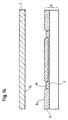
- the method described in Japanese Patent Application Laid Open No. 4-244976 connects to probes (not shown) one ends 12a, 12b of a plurality of printed patterns 10a, 10b to be inspected and collectively couples the other ends 14a, 14b to a non-contact sensor, 16,, as shown in Figure 15.
- the printed patterns are complicated or irregular, e.g., if they branch on the side of the non - contact Sensor 16 as shown in Figure 15B and if one of the branching printed patterns 10c or 10d is open-circuited, an inspection current flows between the probe connected to the end 12b and the non-contact sensor 16 when the other printed pattern 10c or 10d and the printed pattern 10b are not open-circuited. Consequently, the open circuit of the branching portion cannot be detected accurately.
- circuit board refers to a substrate on which wiring can be or has been formed and is not limited in terms of its material, structure, shape, or sizes.
- the circuit board includes, for example, a glass epoxy circuit board, a film-like circuit board, and a package on which circuit elements such as EL CPU are mounted. It also includes a composite circuit board comprising sockets on a glass epoxy circuit board and a circuit board on which circuit elements are mounted.
- wiring refers to a conductor that is used to conduct electricity and is not limited in terms of its material, structure, shape, or sizes. This includes printed patterns, through-holes, and pins that are formed on the circuit board as well as the conducting section of electric cords, sockets, connectors, and pins attached to the circuit board.
- one end of the wiring refers to a point of the wiring to or from which an inspection signal is input or output and that is not limited in terms of its material, structure, shape, or size.
- This includes an electric connection point to which a different component is connected such as an inspection-end or a connector-connection-end of the printed pattern, a connection pin, a pad to which a bonding wire is connected, a pad to which a circuit element or a socket is connected, an insertion portion formed in a socket mounted on the circuit board, and an I/O end of a connector, as well as an arbitrary point within the wiring.
- Coupled refers to coupling two or more members together so that a signal can be transmitted among the members while they are insulated from one another. This includes coupling by means of electrostatic capacity or inductance.
- signal refers to a signal used for inspections and is a concept including either a voltage or a current. It includes an alternating signal such as sine waves, a direct signal, rectangular and triangular signals, and a pulse signal.
- the expression "based on a voltage generated between the first and the second terminals" means that something is based on a voltage generated between the first and the second terminals or a physical quantity corresponding to or associated with the voltage.
- this physical quantity includes not only the voltage but also a current corresponding to or associated with the voltage, and its integrated and differential values.
- detection of the continuity of the wiring includes the detection of an open circuit or shorting in the wiring and the detection of the resistance value of the wiring such as a semi-open-circuit.
- group refers to a set of one or two or more elements.
- signal with rapid changes refers to a signal such as a voltage or a current that is subjected to frequent changes per unit time, and it includes, for example, a direct signal having a step-like rising or falling edge, triangular and a rectangular signals, and a pulse signal.
- electrode section refers to a conductor constituting an electrode on the second electrode side when electrostatic capacity is used for coupling and is not limited in terms of its material, structure, shape or sizes.
- Figure 1 shows the configuration of a bare-board tester that is a circuit-board inspection apparatus according to one embodiment of this invention.
- Figure 2 shows the detailed view of a printed pattern section 34 on an inspected circuit board 32.
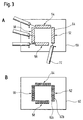
- Figure 3A is a plan view of a sensor module 50.
- Figure 3B is a perspective view of the bottom surface of the sensor module 50 as seen from above.
- Figure 4A is a plan view schematically showing a sensor unit 52.
- Figure 4B is a cross-sectional view schematically showing the integral part of the sensor unit 52.
- Figure 4C is a bottom view schematically showing the sensor unit 52.
- Figure 5A is a plan view schematically showing a sensor unit 52 according to another embodiment.
- Figure 5B is a cross-sectional view schematically showing the integral part of this sensor unit 52.
- Figure 5C is a bottom view schematically showing this sensor unit 52.
- Figure 6A is a plan view schematically showing a sensor unit 52 according to yet another embodiment.
- Figure 6B is a cross-sectional view schematically showing the integral part of this sensor unit 52;
- Figure 6C is a bottom view schematically showing this sensor unit 52.
- FIG. 7A schematically shows the switch section SW1.
- Figure 7B schematically shows the switch section SW2.
- FIG. 8 illustrates signal processing
- Figure 9 is a timing chart showing signal processing.
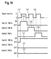
- Figure 10 is a timing chart showing another example of signal processing.
- Figure 11A shows a signal output from a signal source 46 in the example in Figure 10.
- Figure 11B shows a signal output from the signal source 46 in yet another example.
- Figure 12 illustrates signal processing according to another embodiment.
- Figure 13 is a timing chart showing signal processing according to the embodiment in Figure 12.
- Figure 14 illustrates an example of a conventional inspection of the continuity of printed patterns.
- Figure 15A illustrates another example of a conventional inspection of the continuity of printed patterns.
- Figure 15B illustrates yet another example of a conventional inspection of the continuity of printed patterns.
- Figure 1 shows a bare board tester that is a circuit board inspection apparatus according to one embodiment of the present invention.
- This bare board tester inspects the continuity of printed patterns on a printed circuit board (a bare board) before circuit elements are mounted on the board.
- a plurality of printed patterns 34a, 34b, ... are formed on a circuit board 32 and collectively called a printed pattern section 34.
- Pads 36a, 36b, ... are formed at one end of the printed patterns 34a, 34b, ... and collectively called a pad section 36.
- FIG. 2 shows the printed pattern section 34 in detail.
- Pads 38a, 38b, ... are formed at the other ends of the printed patterns 34a, 34b, ... and collectively called a pad section 38.
- the pad section 38 shown in Figure 2 is called a QFP pattern on which QFPs (quad flat packages that are thin and roughly square) are mounted. Thus, the pitch at which the pads 38a, 38b, ... are arranged is very small.
- the pad 38b and the pads 38x, 38y and 38z are connected by the printed pattern 34x to form a ground line.
- the bare board tester includes probes 40a, 40b, ... that are a plurality of first terminals connected to the pads 36a, 36b, ... on the circuit board 32.
- the plurality of probes 40a, 40b, ... is collectively called a probe section 40.
- FIG. 7A schematically shows the switch SW1.
- the switch section SW1 includes a plurality of switches SW1a, SW1b, ... Each switch is turned on and off in response to an instruction from a computer 44 to transmit a signal provided by the signal source 46 to a desired probe in the prove section 40, for example, the probe 40a, as shown in Figure 1 (in this case, only the switch SW1a is turned on)
- the signal transmitted to the probe 40a is provided to the pad 38a (see Figure 2) of the pad section 38 via the pad 36a of the pad section 36 connected to the probe 40a and the printed pattern 34a in the printed pattern section 34.
- a sensor module 50 is located on the pad section 38 on the circuit board 32.
- the sensor module 50 is coupled to the pad section 38 to obtain a signal from the pad section 38 and to supply it to a switch section SW2 that is a second switch means.
- the sensor module 50 comprises a four sensor units 52, 54, 56 and 58 integrally formed. Each sensor unit corresponds to a second terminal. According to this embodiment, the sensor module 50 is composed of a circuit board 60 (see Fig. 4B) that is manufactured through a process similar to the inspected circuit board 32.
- Figures 4A, 4B and 4C schematically shows the sensor unit 52 constituting part of the sensor module 50.
- the sensor unit 52 corresponds to the eight pads 38a, 38b, ... (these eight pads form one group) but is shown to correspond to four pads in Figures 4A, 4B and 4C for the convenience of explanation.
- Figure 4A is a plan view of the sensor unit 52.
- Figure 4B is a cross sectional view showing an integral part.
- Figure 4C is a bottom view.
- electrode plates 62a, 62b, ... constituting an electrode section are independently provided on the bottom surface of the circuit board 60.
- An insulating film 70 is formed to cover the electrode plates 62a, 62b, ...
- the electrode plates 62a, 62b, ... are located opposite to the pads 38a, 38b, ... (see Figure 2) of the pad section 38 of the inspected circuit board 32 which are located to correspond to the sensor unit 52 so as to form a group.
- the electrode plate is designed with nearly the same shape as each pad.
- the electrode 62a and insulating film 70 of the sensor unit 52 and the pad 38a of the inspected circuit board 32 form a capacitor. This is true of the other electrode plates 62b, ...
- connection plate 64 that is a connection conducting section is provided on the top surface of the circuit board 60.
- the connection plate 64 is electrically connected to the electrode plates 62a, 62b, ... via through-holes 66a, 66b, ...
- the connection plate 64 of the sensor unit 52 is capacitively coupled to the group of pads 38a, 38b, ... described above.
- the connection plate 64 is connected to the switch section SW2 via a connection cord 72.
- the connection plate 64 and the through-holes 66a, 66b, ... correspond to connection means.
- shield films 68a and 68b that are shield members are formed on the bottom and top surfaces of the circuit board 60 and connected to each other via a through-hole 68c.
- a ground potential is applied to the shield films 68a and 68b.
- FIG. 3A shows a plan view of the sensor module 50.
- Figure 3B is a perspective view of the bottom surface of the sensor module 50 as seen from above.
- FIG 7B schematically shows the switch section SW2.
- the switch section SW2 comprises four switches SW2a, SW2b, SW2c and SW2d. Each switch is turned on and off in response to an instruction from the computer 44 (see Figure 1) to supply a signal detection section 48 with a signal from a desired one of the four sensor units 52, 54, 56 and 58 constituting the sensor module 50 (in this case, only the switch SW2a is turned on), for example, the sensor unit 52.
- the signal provided by the desired sensor unit 52 is subjected to a predetermined processing in the detection section 48, as shown in Figure 1, and then delivered to the computer 44. Based on the transmitted signal, the computer 44 determines the continuity of a printed pattern selected by the switch sections SW1 and SW2 (in the above example, the printed pattern 34a).
- the computer 44, the signal source 46 and the signal detection section 48 constitute a controller 42.
- the sensor module 50 of the four sensor units 52, 54, 56 and 58 By making the sensor module 50 of the four sensor units 52, 54, 56 and 58 so that a signal can be independently obtained from each sensor unit in this manner, the following advantages can be achieved.
- the pad section 38 (the QFP pattern) of the printed pattern section 34 shown in Figure 2 the pad 38b and the pads 38x, 38y and 38z are connected together by the printed pattern 34x to form a ground line.
- the sensor module of the plurality of sensor units so that a signal can be independently obtained from each sensor unit, complicated or irregular printed patterns can be inspected accurately.
- a single large electrode plate 62 may be provided on the bottom surface of the circuit board 60 as shown in Figures 5A, 5B and 5C. That is, the single large electrode plate 62 of the sensor unit 52 is coupled to the group of pads 38a, 38b, ... (see Figure 2) corresponding to the sensor unit 52.
- This configuration is advantageous because the variation in the electrostatic capacity generated between the electrode plate 62 and the group pads 38a, 38b, ... shown in Figure 2 is relatively small, even if these components are somewhat roughly aligned with one another.
- the above embodiment connects the plurality of electrode plates 62a, 62b, ... to the single connection plate 64 to allow all of the plurality of pads 38a, 38b, ... corresponding to the sensor unit 52 shown in Figure 2 to be subjected to a single signal processing, as shown in Figures 4B and 4A.
- a plurality of connection plates 64a, 64b, ... may be provided on the top surface of the circuit board 60 and connected to the electrode plates 62a, 62b, ... respectively, via the through-holes 66a, 66b, ... to obtain a signal from the connection plates 64a, 64b, ...
- This configuration allows the plurality of pads 38a, 38b, ... shown in Figure 2 to be individually subjected to signal processing. This enables more delicate processing to allow the apparatus to inspect more complicated printed patterns.
- the pads 38a, 38b, ... individually form a group. That is, each group is composed of only a single pad.
- the above embodiment integrates the four sensor units 52, 54, 56, and 58 into the sensor module 50, these sensor units may be separately formed.
- the integration allows the plurality of sensor units to be handled easily compared to when the units are separated.
- the integral sensor module 50 can be more efficiently positioned on the circuit board 32.
- Figure 9 shows an equivalent circuit used for signal processing.
- the signal processing executed by the bare-board tester will be described with reference to Figures 1, 8 and 9. for the sake of convenience, Figure 9 omits the description of a few switches constituting the switch sections SW1 and SW2.
- This embodiment uses a constant-voltage source as the signal source 46 (see (a) in figure 9).
- a constant voltage E is applied to the switch SW1 by the signal source 46, as shown in Figure 1.
- the computer 44 first transmits an instruction to the switch section SW2 to turn on only the switch SW2a while turning off the other switches SW2b, SW2c, and SW2d (see Figures 7B and (b) in Figure 9). Then, only the sensor unit 52 is connected to the signal detection circuit 48, whereas the other sensor units 54, 56, and 58 remain disconnected from the signal detection circuit 48.
- the computer 44 then sends an instruction to the switch SW1 to turn on only the switch SW1a (see (c) in Figure 9) while turning off the other switches SW1b, SW1c, ... (see Figure 7A). Then, only the probe 40a is connected to the signal source 46, whereas the probes 40b, 40c, ... remain disconnected from the signal source 46. This causes the printed pattern 34a on the circuit board 32 to be selected and inspected.
- the resistor R1 represents the internal resistance of the switches SW1a and SW2a
- the resistor R2 represents the resistance of the printed pattern 34a on the circuit board 32.
- the resistor R3 represents the ground resistance in the signal detection section 48.
- the capacitance C1 represents a capacitor formed of the electrode plates 62a, 62b, ... of the sensor unit 52, the insulating film 70 (see Figure 4B), and the pads 38a, 38b, ... corresponding to the sensor unit 52.
- E represents the direct voltage from the signal source 46.
- a peak hold circuit 76 detects and holds its maximum value (corresponding to the voltage Va in (d) in Figure 9).
- the peak hold circuit 76 includes a D/A converter (not shown) that digitalizes and transmits the maximum value to the computer 44. Part of the function of the peak hold circuit 76 can be implemented by the computer 44.
- the computer 44 determines the continuity of the printed pattern 34a on the circuit board 32. For example, it makes a determination by checking whether the maximum value is between the upper and lower reference limits.
- the peak hold circuit 76 can finish detecting the maximum value in a very short time. This enables the continuity of the printed pattern to be determined in a very short time. As a result, the operation is unlikely to be affected by humming noises.
- the computer 44 then transmits an instruction to the switch SW1 to turn the switch SW1b on (see (e) in Figure 9).
- the switch SW1a remains on.
- the probes 40a and 40b are connected to the signal source 46. In this case, the condition of the switch section SW2 remains unchanged.
- the voltage Vx input into the amplifier 74 exhibits a maximum value Vb (see (f) in Figure 9) at almost the exact same time that the switch SW1b is turned on (see (e) in Figure 9).
- the computer 44 determines the continuity of the printed pattern 34b on the circuit board 32 based on the maximum value Vb, as described above.
- the sensor module 50 is composed of the plurality of sensor units 52, 53, ... (see Figure 2), each of which is coupled to the corresponding group of pads via the separate capacitor.
- the electrostatic capacity of each capacitor C1 is relatively small. that is, shown in Equation (1) has a relatively large value (that is, the time constant has a correspondingly small value).
- the time (t) required until the current (i) almost reaches zero is short, as is apparent from Equation (1).
- This embodiment can thus determine the continuity of the printed patterns in short cycles.
- the computer 44 then switches the switches of the switch sections SW1 and SW2 as required to inspect the continuity of the printed patterns 34c, ...
- the circuit board 32 is acceptable, as shown in Figure 9, that is, if the printed patterns 34a, 34b, 34c, ... are not open-circuited , the voltage Vx input to the amplifier 74 is as shown in (d), (f), (g), ..., respectively.
- This embodiment thus allows the continuity of the printed pattern to be inspected promptly and accurately.
- this embodiment turns on the switch SW1b while keeping the switch 1a on (see (c) and (e) in Figure 9), the switch SW1a may be turned off immediately after the peak hold circuit 76 has finished detecting the maximum value for the printed pattern 34a (the maximum value corresponding to the voltage Va), followed by the turning-on of the switch SW1b.
- This configuration eliminates the need to wait for the current (i) flowing through the printed pattern 34a to reach almost zero before starting to inspect the next printed pattern 34b. Thus, the continuity of the printed patterns can be inspected in shorter cycles.
- This configuration also prevents the length of the inspection cycle from being significantly increased even if the time constant (the inverse of ⁇ in Equations (1) and (2)) is large.
- the above embodiment uses the constant-voltage source as the signal source 46 (see (a) in Figure 9) and turns each switch of the switch section SW1 on and off (see (c) and (e) in Figure 9) to obtain a voltage with a step-shaped waveform and sharp rising edges, a circuit that sequentially generates signals with rapid changes may be used as the signal source 46.
- Figure 10 shows a timing chart of signal-processing executed when the signal source 46 described above is used.
- This example employs a rectangular-wave generation circuit as the signal source 46.
- the computer 44 distributes among the printed patterns 34a, 34b, ... each rectangular signal sequentially generated by the signal source 46 ( Figure 11).
- the condition of the voltage Vx input to the amplifier 74 and the processing executed after it has been input to the amplifier 74 are similar to those in the example shown in Figure 9.
- the source 46 may be configured to generate triangular waves as shown in Figure 11A.
- each triangular wave has sharp rising edges (a).
- the signal source 46 may be configured to generate a pulse train as shown in Figure 11B.
- each pulse signal has sharp rising edges (b), as in Figure 11A.
- Signals having sharp rising edges are not limited to those described above. It includes not only those taking no time to rise but also those taking a little time to do. It also includes those having sharp falling edges.
- this invention determines the continuity of the wiring based on the maximum voltage generated at the second terminal after the signal has changed rapidly
- This invention may be configured to determine the continuity of the wiring based on a quantity relating to the voltage generated between the first and second terminals when a signal with rapid changes is applied, such as the average of the voltage within a specified period of time, the voltage value obtained after a specified period of time, the steady-state deviation voltage, or the maximum, average, or integral value of the current flowing between the first and second terminals, all values obtained after the signal has changed rapidly.
- the continuity of the wiring can be determined in a shorter time by determining it based on the maximum voltage, as in the above embodiment.
- a sine-wave generator for example, may be used as the signal source 46, as shown in Figure 12.
- a sine wave with a frequency of approximately 10 MHz is generated by the signal source 46.
- the signal detection section 48 may be composed of a waveform observation circuit 80 instead of the peak hold circuit 76 in Figure 8.
- the wave observation circuit 80 is a circuit for processing an input signal and evaluating its level and waveform such as that from a wave detector or an oscilloscope.
- the computer 44 turns each of the switches SW1 and SW2 on and off as required (see (b) in Figure 13) to distribute among the printed patterns 34a, 34b, 34c, ... a sine wave generated by the signal source 46 (see (a) in Figure 13), while determining the continuity of each printed pattern based on the data obtained via the signal detection section 48, as shown in Figure 13.
- the voltage Vx input to the amplifier 74 is as shown in (c).
- the voltage Vx is as shown in (d). That is, the open circuit of the printed pattern can be determined easily because it reduces the input level of the signal to a very small value.
- the printed pattern 34c is open-circuited though the printed patterns 34a and 34b are not, so this circuit board 32 is determined to be unacceptable.
- alternating signal If such an alternating signal is used, inspections cannot be conducted as promptly as in the embodiment using a signal with rapid changes.
- the use of such an alternating signal allows the apparatus to be composed of a circuit such as a sine-wave generator or a wave detector that is relatively often used for a non-contact inspection apparatus.
- the use of such a signal is thus expected to reduce the design cost of the apparatus and the time required for delivery, as well as to reduce the manufacturing cost of the apparatus by allowing existing parts to be used for it.
- Part or all of the functions of the computer 44 shown in Figure 1 can also be implemented using hardware logic.
- part or all of the functions of the signal source 46 or the signal detection section 48 can also be implemented using the computer.
- the shield members may be eliminated.
- the use of the shield members can reduce noise.
- the above embodiment provides on the second terminal insulating film covering the electrode section, the insulating film may be eliminated. By providing insulating film on the second terminal, however, inspections can be conducted promptly, as the need to prepare separate insulating films prior to inspection is eliminated.
- connection-conducting section on the other side may be eliminated.
- the structure of the sensor module can be simplified, as a signal can be transmitted easily via this section.
- the sensor module is composed of the circuit board that is manufactured by a process similar to that used for the inspected circuit board, it may be made of a circuit board that is manufactured by a process dissimilar to that used for the inspected circuit board, or may be configured without a circuit board.
- the second terminal is capacitively coupled to the other end of the wiring, it may be inductively coupled to this other end.
- the capacitive coupling enables reliable inspections to be conducted using a simple configuration.
- the first terminal may be capacitively connected to one end of the wiring.
- the above embodiment provides a plurality of first terminals and uses the first switch means to select a desired first terminal in order to select one of the one ends of the wiring on the inspected circuit board, only one first terminal may be provided and the inspected circuit board may be moved relative to this first terminal to select one of the ends of the wiring.
- the former configuration eliminates the need to move the inspected circuit board relative to the first terminal, thereby enabling inspections to be conducted very accurately, reducing the manufacturing cost of the apparatus, and allowing inspections to be automated easily.
- this invention is not limited to such a tester.
- This invention is applicable to general circuit board inspection apparatuses and methods, such as those in which a circuit board on which circuit elements such as a CPU are mounted or a package on which circuit elements are mounted is inspected.
Landscapes
- Engineering & Computer Science (AREA)
- Microelectronics & Electronic Packaging (AREA)
- General Engineering & Computer Science (AREA)
- Physics & Mathematics (AREA)
- General Physics & Mathematics (AREA)
- Testing Of Short-Circuits, Discontinuities, Leakage, Or Incorrect Line Connections (AREA)
Applications Claiming Priority (3)
| Application Number | Priority Date | Filing Date | Title |
|---|---|---|---|
| JP4611497 | 1997-02-28 | ||
| JP46114/97 | 1997-02-28 | ||
| JP09046114A JP3080595B2 (ja) | 1997-02-28 | 1997-02-28 | 基板検査装置および基板検査方法 |
Publications (3)
| Publication Number | Publication Date |
|---|---|
| EP0862062A2 true EP0862062A2 (fr) | 1998-09-02 |
| EP0862062A3 EP0862062A3 (fr) | 2000-02-02 |
| EP0862062B1 EP0862062B1 (fr) | 2002-11-13 |
Family
ID=12737984
Family Applications (1)
| Application Number | Title | Priority Date | Filing Date |
|---|---|---|---|
| EP98103455A Expired - Lifetime EP0862062B1 (fr) | 1997-02-28 | 1998-02-27 | Procédé et dispositif de contrôle de cartes de circuit |
Country Status (4)
| Country | Link |
|---|---|
| US (1) | US6097202A (fr) |
| EP (1) | EP0862062B1 (fr) |
| JP (1) | JP3080595B2 (fr) |
| DE (1) | DE69809313T2 (fr) |
Cited By (2)
| Publication number | Priority date | Publication date | Assignee | Title |
|---|---|---|---|---|
| WO2009056820A1 (fr) * | 2007-10-31 | 2009-05-07 | Qrg Limited | Appareil et procédé de test |
| CN110619726A (zh) * | 2019-10-09 | 2019-12-27 | 苏州南师大科技园投资管理有限公司 | 一种用于信息技术防盗用安全监控装置 |
Families Citing this family (33)
| Publication number | Priority date | Publication date | Assignee | Title |
|---|---|---|---|---|
| US20020053734A1 (en) | 1993-11-16 | 2002-05-09 | Formfactor, Inc. | Probe card assembly and kit, and methods of making same |
| US6483328B1 (en) | 1995-11-09 | 2002-11-19 | Formfactor, Inc. | Probe card for probing wafers with raised contact elements |
| JP3006558B2 (ja) * | 1997-08-22 | 2000-02-07 | 日本電気株式会社 | フォトマスクの帯電防止方法およびそれに用いる装置 |
| IL124961A (en) | 1998-06-16 | 2006-10-05 | Orbotech Ltd | Contactless test method and system |
| JP4277398B2 (ja) * | 1999-03-26 | 2009-06-10 | 富士通株式会社 | 配線板の検査装置 |
| US6420878B1 (en) * | 1999-11-12 | 2002-07-16 | Agilent Technologies, Inc. | System and method of integrated circuit self-testing of circuit board connectors |
| JP2001153921A (ja) * | 1999-11-29 | 2001-06-08 | Ando Electric Co Ltd | 波形観測治具および波形観測装置 |
| JP2001221824A (ja) * | 2000-02-10 | 2001-08-17 | Oht Inc | 検査装置及び検査方法、検査ユニット |
| JP2001228192A (ja) * | 2000-02-18 | 2001-08-24 | Oht Inc | 検査装置及び検査装置の保持具 |
| JP2001235501A (ja) * | 2000-02-22 | 2001-08-31 | Oht Inc | 検査装置及びセンサ |
| US6330516B1 (en) * | 2000-03-27 | 2001-12-11 | Power Distribution, Inc. | Branch circuit monitor |
| JP2002311075A (ja) * | 2000-06-16 | 2002-10-23 | Oht Inc | 回路基板の検査装置及び検査方法 |
| JP2002156399A (ja) * | 2000-11-17 | 2002-05-31 | Oht Inc | 回路基板の検査装置及び検査方法 |
| JP2002156417A (ja) * | 2000-11-17 | 2002-05-31 | Oht Inc | 回路基板の検査装置及び検査方法 |
| US7562350B2 (en) * | 2000-12-15 | 2009-07-14 | Ricoh Company, Ltd. | Processing system and method using recomposable software |
| WO2002086520A1 (fr) * | 2001-04-19 | 2002-10-31 | Oht Inc. | Appareil d'inspection et procede d'inspection |
| US6600332B2 (en) * | 2001-08-16 | 2003-07-29 | Aiptek International Inc. | Tablet with short testing function and method of measuring |
| US20040234121A1 (en) * | 2001-08-27 | 2004-11-25 | Tatsuhisa Fujii | Circuit wiring inspetion instrument and circuit wiring inspecting method |
| JP4623887B2 (ja) * | 2001-08-27 | 2011-02-02 | オー・エイチ・ティー株式会社 | 検査装置用センサ及び検査装置 |
| US6573728B2 (en) | 2001-08-29 | 2003-06-03 | International Business Machines Corporation | Method and circuit for electrical testing of isolation resistance of large capacitance network |
| JP2003098212A (ja) * | 2001-09-20 | 2003-04-03 | Oht Inc | 検査装置並びに検査方法 |
| JP2003098213A (ja) * | 2001-09-20 | 2003-04-03 | Oht Inc | 検査装置並びに検査方法 |
| US6947853B2 (en) * | 2002-05-23 | 2005-09-20 | Oht, Inc. | Apparatus and method for inspecting electrical continuity of circuit board, jig for use therein, and recording medium thereon |
| US6999888B2 (en) * | 2002-09-30 | 2006-02-14 | Intel Corporation | Automated circuit board test actuator system |
| US7154257B2 (en) * | 2002-09-30 | 2006-12-26 | Intel Corporation | Universal automated circuit board tester |
| US7250781B2 (en) * | 2002-12-19 | 2007-07-31 | Fuji Xerox Co., Ltd. | Circuit board inspection device |
| JP4124337B2 (ja) * | 2003-01-17 | 2008-07-23 | ヤマハファインテック株式会社 | プリント基板の検査装置 |
| US6933730B2 (en) * | 2003-10-09 | 2005-08-23 | Agilent Technologies, Inc. | Methods and apparatus for testing continuity of electrical paths through connectors of circuit assemblies |
| US7323897B2 (en) * | 2004-12-16 | 2008-01-29 | Verigy (Singapore) Pte. Ltd. | Mock wafer, system calibrated using mock wafer, and method for calibrating automated test equipment |
| US7453267B2 (en) * | 2005-01-14 | 2008-11-18 | Power Measurement Ltd. | Branch circuit monitor system |
| US20080258704A1 (en) * | 2007-04-23 | 2008-10-23 | Ryskoski Matthew S | Method and apparatus for identifying broken pins in a test socket |
| JP6076178B2 (ja) * | 2013-04-02 | 2017-02-08 | ホリゾン・インターナショナル株式会社 | 断裁機 |
| US9121884B2 (en) | 2013-06-07 | 2015-09-01 | Infineon Technologies Ag | Capacitive test method, apparatus and system for semiconductor packages |
Family Cites Families (14)
| Publication number | Priority date | Publication date | Assignee | Title |
|---|---|---|---|---|
| DE3038665C2 (de) * | 1980-10-13 | 1990-03-29 | Riba-Prüftechnik GmbH, 7801 Schallstadt | Prüfeinrichtung zum Überprüfen von mit Leiterbahnen versehenen Leiterplatten |
| US4565966A (en) * | 1983-03-07 | 1986-01-21 | Kollmorgen Technologies Corporation | Method and apparatus for testing of electrical interconnection networks |
| GB2143954A (en) * | 1983-07-22 | 1985-02-20 | Sharetree Ltd | A capacitive method and apparatus for checking connections of a printed circuit board |
| US5006808A (en) * | 1989-03-21 | 1991-04-09 | Bath Scientific Limited | Testing electrical circuits |
| US5023545A (en) * | 1990-06-04 | 1991-06-11 | The United States Of America | Circuit probing system |
| US5625292A (en) * | 1990-12-20 | 1997-04-29 | Hewlett-Packard Company | System for measuring the integrity of an electrical contact |
| US5198756A (en) * | 1991-07-29 | 1993-03-30 | Atg-Electronics Inc. | Test fixture wiring integrity verification device |
| US5187430A (en) * | 1991-08-30 | 1993-02-16 | Compaq Computer Corporation | Method and apparatus for determining nets among nodes in a circuit board |
| US5266901A (en) * | 1992-05-29 | 1993-11-30 | International Business Machines Corp. | Apparatus and method for resistive detection and waveform analysis of interconenction networks |
| US5420500A (en) * | 1992-11-25 | 1995-05-30 | Hewlett-Packard Company | Pacitive electrode system for detecting open solder joints in printed circuit assemblies |
| IT1261074B (it) * | 1993-07-05 | 1996-05-08 | Luciano Bonaria | Metodo e dispositivo di collaudo per schede elettroniche |
| US5426372A (en) * | 1993-07-30 | 1995-06-20 | Genrad, Inc. | Probe for capacitive open-circuit tests |
| US5747999A (en) * | 1994-08-15 | 1998-05-05 | Okano Hitech Co., Ltd. | Feed control element used in substrate inspection and method and apparatus for inspecting substrates |
| JP3617013B2 (ja) * | 1994-08-15 | 2005-02-02 | オー・エイチ・ティー株式会社 | 電子回路基板の検査装置及び電子回路の検査方法 |
-
1997
- 1997-02-28 JP JP09046114A patent/JP3080595B2/ja not_active Expired - Lifetime
-
1998
- 1998-02-27 US US09/032,239 patent/US6097202A/en not_active Expired - Lifetime
- 1998-02-27 EP EP98103455A patent/EP0862062B1/fr not_active Expired - Lifetime
- 1998-02-27 DE DE69809313T patent/DE69809313T2/de not_active Expired - Fee Related
Cited By (2)
| Publication number | Priority date | Publication date | Assignee | Title |
|---|---|---|---|---|
| WO2009056820A1 (fr) * | 2007-10-31 | 2009-05-07 | Qrg Limited | Appareil et procédé de test |
| CN110619726A (zh) * | 2019-10-09 | 2019-12-27 | 苏州南师大科技园投资管理有限公司 | 一种用于信息技术防盗用安全监控装置 |
Also Published As
| Publication number | Publication date |
|---|---|
| JP3080595B2 (ja) | 2000-08-28 |
| DE69809313D1 (de) | 2002-12-19 |
| JPH10239371A (ja) | 1998-09-11 |
| DE69809313T2 (de) | 2003-07-10 |
| US6097202A (en) | 2000-08-01 |
| EP0862062A3 (fr) | 2000-02-02 |
| EP0862062B1 (fr) | 2002-11-13 |
Similar Documents
| Publication | Publication Date | Title |
|---|---|---|
| US6097202A (en) | Circuit board inspection apparatus and method | |
| US5969530A (en) | Circuit board inspection apparatus and method employing a rapidly changing electrical parameter signal | |
| US5517110A (en) | Contactless test method and system for testing printed circuit boards | |
| US5420500A (en) | Pacitive electrode system for detecting open solder joints in printed circuit assemblies | |
| US6930494B2 (en) | Capacitive probe assembly with flex circuit | |
| US5625292A (en) | System for measuring the integrity of an electrical contact | |
| US6462556B2 (en) | Circuit board testing apparatus and method | |
| US6734681B2 (en) | Apparatus and methods for testing circuit boards | |
| US6353327B2 (en) | Circuit board misalignment detection apparatus and method | |
| JP3361311B2 (ja) | 基板検査装置および基板検査方法 | |
| JPH10142291A (ja) | Ic試験装置 | |
| JPH11153638A (ja) | 基板検査装置および基板検査方法 | |
| JP4200182B2 (ja) | 回路基板検査装置 | |
| CN220650802U (zh) | 一种用于检测被测装置中的电气缺陷的传感器装置 | |
| JPH11133090A (ja) | 基板検査装置および基板検査方法 | |
| JP2000074975A (ja) | 基板検査装置および基板検査方法 | |
| JPS62269075A (ja) | プリント基板検査装置 | |
| JP4292013B2 (ja) | 回路基板検査装置 | |
| JP3076424B2 (ja) | 回路基板検査方法と検査基板並びに回路基板検査装置 | |
| JP3717502B2 (ja) | 検査装置及び検査方法 | |
| JPH04252964A (ja) | テスターヘッド | |
| JP2004144760A (ja) | 検査装置及び検査方法 | |
| JP2004085584A (ja) | 検査装置及び検査方法 |
Legal Events
| Date | Code | Title | Description |
|---|---|---|---|
| PUAI | Public reference made under article 153(3) epc to a published international application that has entered the european phase |
Free format text: ORIGINAL CODE: 0009012 |
|
| AK | Designated contracting states |
Kind code of ref document: A2 Designated state(s): DE FR GB |
|
| AX | Request for extension of the european patent |
Free format text: AL;LT;LV;MK;RO;SI |
|
| PUAL | Search report despatched |
Free format text: ORIGINAL CODE: 0009013 |
|
| AK | Designated contracting states |
Kind code of ref document: A3 Designated state(s): AT BE CH DE DK ES FI FR GB GR IE IT LI LU MC NL PT SE |
|
| AX | Request for extension of the european patent |
Free format text: AL;LT;LV;MK;RO;SI |
|
| 17P | Request for examination filed |
Effective date: 20000717 |
|
| AKX | Designation fees paid |
Free format text: DE FR GB |
|
| 17Q | First examination report despatched |
Effective date: 20010906 |
|
| GRAG | Despatch of communication of intention to grant |
Free format text: ORIGINAL CODE: EPIDOS AGRA |
|
| GRAG | Despatch of communication of intention to grant |
Free format text: ORIGINAL CODE: EPIDOS AGRA |
|
| GRAH | Despatch of communication of intention to grant a patent |
Free format text: ORIGINAL CODE: EPIDOS IGRA |
|
| GRAH | Despatch of communication of intention to grant a patent |
Free format text: ORIGINAL CODE: EPIDOS IGRA |
|
| GRAA | (expected) grant |
Free format text: ORIGINAL CODE: 0009210 |
|
| AK | Designated contracting states |
Kind code of ref document: B1 Designated state(s): DE FR GB |
|
| PG25 | Lapsed in a contracting state [announced via postgrant information from national office to epo] |
Ref country code: FR Free format text: LAPSE BECAUSE OF FAILURE TO SUBMIT A TRANSLATION OF THE DESCRIPTION OR TO PAY THE FEE WITHIN THE PRESCRIBED TIME-LIMIT Effective date: 20021113 |
|
| REG | Reference to a national code |
Ref country code: GB Ref legal event code: FG4D |
|
| REF | Corresponds to: |
Ref document number: 69809313 Country of ref document: DE Date of ref document: 20021219 |
|
| PGFP | Annual fee paid to national office [announced via postgrant information from national office to epo] |
Ref country code: GB Payment date: 20030211 Year of fee payment: 6 |
|
| EN | Fr: translation not filed | ||
| PLBE | No opposition filed within time limit |
Free format text: ORIGINAL CODE: 0009261 |
|
| STAA | Information on the status of an ep patent application or granted ep patent |
Free format text: STATUS: NO OPPOSITION FILED WITHIN TIME LIMIT |
|
| 26N | No opposition filed |
Effective date: 20030814 |
|
| PG25 | Lapsed in a contracting state [announced via postgrant information from national office to epo] |
Ref country code: GB Free format text: LAPSE BECAUSE OF NON-PAYMENT OF DUE FEES Effective date: 20040227 |
|
| GBPC | Gb: european patent ceased through non-payment of renewal fee | ||
| PGFP | Annual fee paid to national office [announced via postgrant information from national office to epo] |
Ref country code: DE Payment date: 20060222 Year of fee payment: 9 |
|
| PG25 | Lapsed in a contracting state [announced via postgrant information from national office to epo] |
Ref country code: DE Free format text: LAPSE BECAUSE OF NON-PAYMENT OF DUE FEES Effective date: 20070901 |