EP0862326A2 - Appareil d'enregistrement et de reproduction de données - Google Patents
Appareil d'enregistrement et de reproduction de données Download PDFInfo
- Publication number
- EP0862326A2 EP0862326A2 EP98103283A EP98103283A EP0862326A2 EP 0862326 A2 EP0862326 A2 EP 0862326A2 EP 98103283 A EP98103283 A EP 98103283A EP 98103283 A EP98103283 A EP 98103283A EP 0862326 A2 EP0862326 A2 EP 0862326A2
- Authority
- EP
- European Patent Office
- Prior art keywords
- character
- display
- memory
- image
- data
- Prior art date
- Legal status (The legal status is an assumption and is not a legal conclusion. Google has not performed a legal analysis and makes no representation as to the accuracy of the status listed.)
- Withdrawn
Links
- 230000015654 memory Effects 0.000 claims abstract description 58
- 238000010586 diagram Methods 0.000 description 7
- 238000000034 method Methods 0.000 description 7
- 238000007906 compression Methods 0.000 description 4
- 230000006835 compression Effects 0.000 description 4
- 239000003086 colorant Substances 0.000 description 1
- 238000013144 data compression Methods 0.000 description 1
- 239000004973 liquid crystal related substance Substances 0.000 description 1
- 239000011159 matrix material Substances 0.000 description 1
- 239000004065 semiconductor Substances 0.000 description 1
- 239000007787 solid Substances 0.000 description 1
Images



Classifications
-
- G—PHYSICS
- G09—EDUCATION; CRYPTOGRAPHY; DISPLAY; ADVERTISING; SEALS
- G09G—ARRANGEMENTS OR CIRCUITS FOR CONTROL OF INDICATING DEVICES USING STATIC MEANS TO PRESENT VARIABLE INFORMATION
- G09G5/00—Control arrangements or circuits for visual indicators common to cathode-ray tube indicators and other visual indicators
- G09G5/36—Control arrangements or circuits for visual indicators common to cathode-ray tube indicators and other visual indicators characterised by the display of a graphic pattern, e.g. using an all-points-addressable [APA] memory
- G09G5/39—Control of the bit-mapped memory
- G09G5/393—Arrangements for updating the contents of the bit-mapped memory
-
- H—ELECTRICITY
- H04—ELECTRIC COMMUNICATION TECHNIQUE
- H04N—PICTORIAL COMMUNICATION, e.g. TELEVISION
- H04N23/00—Cameras or camera modules comprising electronic image sensors; Control thereof
- H04N23/60—Control of cameras or camera modules
- H04N23/63—Control of cameras or camera modules by using electronic viewfinders
-
- H—ELECTRICITY
- H04—ELECTRIC COMMUNICATION TECHNIQUE
- H04N—PICTORIAL COMMUNICATION, e.g. TELEVISION
- H04N5/00—Details of television systems
- H04N5/222—Studio circuitry; Studio devices; Studio equipment
- H04N5/262—Studio circuits, e.g. for mixing, switching-over, change of character of image, other special effects ; Cameras specially adapted for the electronic generation of special effects
- H04N5/278—Subtitling
-
- H—ELECTRICITY
- H04—ELECTRIC COMMUNICATION TECHNIQUE
- H04N—PICTORIAL COMMUNICATION, e.g. TELEVISION
- H04N5/00—Details of television systems
- H04N5/44—Receiver circuitry for the reception of television signals according to analogue transmission standards
- H04N5/46—Receiver circuitry for the reception of television signals according to analogue transmission standards for receiving on more than one standard at will
-
- H—ELECTRICITY
- H04—ELECTRIC COMMUNICATION TECHNIQUE
- H04N—PICTORIAL COMMUNICATION, e.g. TELEVISION
- H04N5/00—Details of television systems
- H04N5/76—Television signal recording
- H04N5/765—Interface circuits between an apparatus for recording and another apparatus
- H04N5/77—Interface circuits between an apparatus for recording and another apparatus between a recording apparatus and a television camera
- H04N5/772—Interface circuits between an apparatus for recording and another apparatus between a recording apparatus and a television camera the recording apparatus and the television camera being placed in the same enclosure
-
- H—ELECTRICITY
- H04—ELECTRIC COMMUNICATION TECHNIQUE
- H04N—PICTORIAL COMMUNICATION, e.g. TELEVISION
- H04N5/00—Details of television systems
- H04N5/44—Receiver circuitry for the reception of television signals according to analogue transmission standards
- H04N5/445—Receiver circuitry for the reception of television signals according to analogue transmission standards for displaying additional information
-
- H—ELECTRICITY
- H04—ELECTRIC COMMUNICATION TECHNIQUE
- H04N—PICTORIAL COMMUNICATION, e.g. TELEVISION
- H04N5/00—Details of television systems
- H04N5/76—Television signal recording
- H04N5/907—Television signal recording using static stores, e.g. storage tubes or semiconductor memories
-
- H—ELECTRICITY
- H04—ELECTRIC COMMUNICATION TECHNIQUE
- H04N—PICTORIAL COMMUNICATION, e.g. TELEVISION
- H04N9/00—Details of colour television systems
- H04N9/64—Circuits for processing colour signals
- H04N9/642—Multi-standard receivers
-
- H—ELECTRICITY
- H04—ELECTRIC COMMUNICATION TECHNIQUE
- H04N—PICTORIAL COMMUNICATION, e.g. TELEVISION
- H04N9/00—Details of colour television systems
- H04N9/79—Processing of colour television signals in connection with recording
- H04N9/80—Transformation of the television signal for recording, e.g. modulation, frequency changing; Inverse transformation for playback
- H04N9/804—Transformation of the television signal for recording, e.g. modulation, frequency changing; Inverse transformation for playback involving pulse code modulation of the colour picture signal components
- H04N9/8042—Transformation of the television signal for recording, e.g. modulation, frequency changing; Inverse transformation for playback involving pulse code modulation of the colour picture signal components involving data reduction
-
- H—ELECTRICITY
- H04—ELECTRIC COMMUNICATION TECHNIQUE
- H04N—PICTORIAL COMMUNICATION, e.g. TELEVISION
- H04N9/00—Details of colour television systems
- H04N9/79—Processing of colour television signals in connection with recording
- H04N9/87—Regeneration of colour television signals
- H04N9/8715—Regeneration of colour television signals involving the mixing of the reproduced video signal with a non-recorded signal, e.g. a text signal
Definitions
- the present invention relates to image recording and reproduction apparatuses, and more particularly, to an image recording and reproduction apparatus that can operate in a first display mode for displaying a first display screen in which an image is constituted by a first number of horizontal scanning lines and a second display mode for displaying a second display screen in which an image is constituted by a second greater number of horizontal scanning lines.
- a digital still camera is an electronic image recording and reproduction apparatus that can record and store image data obtained from a solid state image sensing device such as a CCD onto a recording medium such as a semiconductor memory and view a reproduced image through a display device such as a liquid crystal display device (LCD).
- a solid state image sensing device such as a CCD
- a recording medium such as a semiconductor memory
- a display device such as a liquid crystal display device (LCD).
- Fig. 4 is a circuit block diagram showing a structure of a conventional digital still camera.
- a conventional still camera includes a CCD 1, a CDS/AGC circuit 2, an A/D converter 3, a signal processing circuit 4, an image compression circuit 5 and an image memory 6.
- the still camera also includes an image expansion circuit 7, a display memory 8, a display circuit 9, an D/A converter 10, an LCD 11, a character data set circuit 21, a switch 22, an NTSC character font memory 23, and a PAL character font memory 24.
- D/A converter 10 can be connected to an external monitor device by means of a connector and the like.
- Incident light through a lens not shown is converted into an analog image signal by CCD 1.
- the signal output from CCD 1 has its level adjusted by CDS/AGC circuit 2, and then converted into a digital signal by A/D converter 3.
- the data amount matches the number of pixels of CCD 1.
- One color data corresponding to a color filter of CCD 1 is present per one pixel.
- the signal output from A/D converter 3 is subjected to various processes such as pixel interpolation and matrix processing by signal processing circuit 4 to be converted into image data of Y, U and V. These image data are provided for each of all the pixels.
- Y corresponds to a luminance signal
- U and V correspond to two types of color difference signals.
- the image data is compressed by image compression circuit 5 and recorded into image memory 6.
- the screen is divided into a plurality of blocks of 8 ⁇ 8 pixels as shown in Fig. 5.
- Data compression is carried out for each component of Y, U and V on a block-by-block basis.
- the compressed data is read out from image memory 6.
- the readout data is expanded into the former Y, U and V data by image expansion circuit 7 to be written into display memory 8.
- characters of numerics and signs are also written into display memory 8.
- switch 22 is altered according to whether the monitor device complies with the NTSC method or the PAL method, whereby the appropriate NTSC character font memory 23 or PAL character font memory 24 is connected to character data set circuit 21.
- Character data set circuit 21 reads out the character data from the connected memory 23 or 24 to provide the read out data into display memory 8.
- the image data and character data in display memory 8 are read out by display circuit 9 to be converted into analog signals by D/A converter 10.
- the converted analog signals are provided to LCD 11 and an external monitor device.
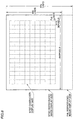
- Switching is provided between character font memory 23 and 24 depending upon whether the monitor device complies with the NTSC system or the PAL system because the vertical to horizontal ratio of the display screen differs depending upon the system of the monitor device. More specifically, as shown in Fig. 6, an image is formed of 480 lines in the vertical direction and 640 pixels (dots) in the horizontal direction in the NTSC system. In the PAL system, an image is formed of 570 lines in the vertical direction and 640 pixels in the horizontal direction.
- arrangement is provided so that the position of the characters in the display screen does not differ according to the system employed by the monitor device by arranging the character image formed of 46 lines ⁇ 36 pixels in 9 rows and 15 columns at the middle of display screen for a monitor device of the NTSC system and a character image formed of 54 lines ⁇ 36 pixels in 9 rows and 15 columns at the middle of the display screen for a monitor device of the PAL system.
- the horizontal scanning lines are skipped in Fig. 6 although there are 525 lines and 625 lines in the vertical direction in the NTSC system and the PAL system, respectively.
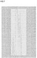
- font data as shown in Fig. 7 is prepared.
- This example of Fig. 7 shows the display of the alphabet letter "I" in 36 pixels ⁇ 46 lines.
- a white character "I” is formed within a black rectangle.
- display circuit 9 includes character level set registers 31-33, a character level select circuit 34, and switches 35 and 36.
- Character level set registers 31-33 provides levels 1-3 corresponding to the color to be displayed by respective pixels.
- the three switch terminals 35a-35c of switch 35 receive the outputs from character level set registers 31-33, respectively.
- Switch 36 has one switch terminal 36a receiving the output of display memory 8 and the other switch terminal 36b connected to a common terminal 35d of switch 35.
- a common terminal 36c of switch 36 is connected to D/A converter 10. Switches 35 and 36 are controlled by character level select circuit 34.
- the character data corresponding to the less significant 2 bits of each U and V data in display memory 8 takes four types of values from 0-3 including the above-described 1, 2.
- connection across terminals 36a and 36c of switch 36 is established so that the background image data in display memory 8 is applied to D/A converter 10.
- character data is 1-3, the connection across terminals 36b and 36c of switch 36 is established, so that the outputs of character level set registers 31-33 are applied to D/A converter 10.
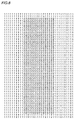
- a display of a character such as that shown in Fig. 7 can be provided.
- the conventional digital still camera had the disadvantage that a relatively great memory capacity is required since two types of character fonts for both the NTSC and PAL systems had to be prepared.
- a main object of the present invention is to provide an image recording and reproduction apparatus that can provide character display on a display screen of two systems with a small memory capacity.
- an image recording and reproduction apparatus has character image read out from a memory device directly provided on a display screen when in a first display mode and has the number of dots in the vertical direction of the character image read out from the memory device increased and then provided on a display screen when in a second display mode. It is therefore not necessary to provide separate character images for the first display mode and for the second display mode.
- the capacity of the memory device can be reduced.
- the ratio of the number of dots in the vertical direction of a character image displayed in the first and second display modes is equal to the ratio of the number of horizontal scanning lines in the first and second display modes. Therefore, the character image can be provided on a display screen at the same position in the first and second display modes.
- Fig. 1 is a block diagram showing a structure of a digital still camera according to a first embodiment of the present invention.
- Figs. 2 and 3 are flow charts showing the former half and latter half, respectively, of the processing operation of a character font readout control circuit of Fig. 1.
- Fig. 4 is a circuit block diagram showing a structure of a conventional digital still camera.
- Fig. 5 is a diagram for describing an operation of an image compression circuit shown in Fig. 4.
- Fig. 6 is a diagram for describing the difference between the NTSC method and the PAL method.
- Fig. 7 shows an example of font data stored in the NTSC character font memory of Fig. 4.
- Fig. 8 shows a character displayed according to the font data of Fig. 7.
- Fig. 9 is a circuit block diagram showing a structure of a display circuit of Fig. 4.
- a character font memory 23 for the NTSC in which one character is formed of 46 lines is provided.
- the monitor device complies with the PAL system
- data identical to one preceding line is written into display memory 8 for every 5 lines. Therefore, one character can be displayed in 54 lines which is an increase of 8 lines in the vertical direction per one character.
- the two display systems can be accommodated by one memory 23.
- the total memory capacity can be reduced than that of the conventional case where two memories 23 and 24 are required.
- Fig. 1 is a circuit block diagram showing a structure of a digital still camera according to an embodiment of the present invention.
- the digital still camera of the present invention differs from the conventional digital still camera of Fig. 4 in that switch 22 and PAL character font memory 24 are removed, and that a character font readout control circuit 20 is newly provided.
- character font readout control circuit 20 controls character data set circuit 21 so that the character data in NTSC character font memory 23 is written into display memory 8 as in the conventional manner.
- character font readout control circuit 20 controls character data set circuit 21 so that 5 lines of character data are written into display memory 8, and then the character data of the fifth line is written again into the sixth line of display memory 8.
- step S1 character font readout control circuit 20 determines whether the monitor device connected to the digital still camera complies with the NTSC system or the PAL system. When in the NTSC system, the control proceeds to step S2 where the number of lines "line_max" forming a character is set to 46. When in the PAL system, control proceeds to step S3 to set the number of lines "line_max" forming a character to 54.
- character font readout control circuit 20 sets the number of lines "row” of the character to be displayed in one screen to 0.
- determination is made whether the value of "row” is smaller than 9 or not. When “row” is not smaller than 9, the operation ends. When “row” is smaller than 9, control proceeds to step S6.
- step S6 character font readout control circuit 20 sets the number of columns "col” of the character to be displayed in one screen to 0.
- step S8 determination is made that "col” is smaller than 15 at step S7, the control proceeds to step S8.
- step S8 character font readout control circuit 20 sets the number of lines "i" of one character to 0.
- step S10 character font readout control circuit 20 sets the number of pixels of a horizontal line in one character to 0.
- step S11 determination is made whether the number of pixels "j" is smaller than 36.
- step S12 the character data of font memory 23 is written into display memory 8 at a predetermined address under control of character data set circuit 21.
- step S13 the addresses of display memory 8 and font memory 23 are updated to one pixel rightwards, and the number of pixels "j" is incremented (+1). Then, control returns to step S11.
- step S15 determination is made whether the line number is any of 5, 10, 15, 20, 25, 30, 35, and 40, i.e. whether "i" is a multiple of 5.
- step S18 determination is made whether the line number is any of 5, 10, 15, 20, 25, 30, 35, and 40, i.e. whether "i" is a multiple of 5.
- step S18 determination is made whether the line number is any of 5, 10, 15, 20, 25, 30, 35, and 40, i.e. whether "i" is a multiple of 5.
- step S18 determines whether the line number is any of 5, 10, 15, 20, 25, 30, 35, and 40, i.e. whether "i" is a multiple of 5.
- step S18 the control proceeds to step S16 where the address of display memory 8 is updated to the beginning of the next line and the address of font memory 23 is updated to the beginning of the currently set line.
- step S17 the character data in font memory 23 is written into display memory 8 at a predetermined position under control of character data set circuit 21.
Landscapes
- Engineering & Computer Science (AREA)
- Multimedia (AREA)
- Signal Processing (AREA)
- Physics & Mathematics (AREA)
- Computer Hardware Design (AREA)
- General Physics & Mathematics (AREA)
- Theoretical Computer Science (AREA)
- Television Signal Processing For Recording (AREA)
- Studio Devices (AREA)
- Television Systems (AREA)
- Controls And Circuits For Display Device (AREA)
- Studio Circuits (AREA)
Applications Claiming Priority (3)
| Application Number | Priority Date | Filing Date | Title |
|---|---|---|---|
| JP4235797 | 1997-02-26 | ||
| JP09042357A JP3101580B2 (ja) | 1997-02-26 | 1997-02-26 | 画像記録再生装置 |
| JP42357/97 | 1997-02-26 |
Publications (2)
| Publication Number | Publication Date |
|---|---|
| EP0862326A2 true EP0862326A2 (fr) | 1998-09-02 |
| EP0862326A3 EP0862326A3 (fr) | 1999-12-01 |
Family
ID=12633793
Family Applications (1)
| Application Number | Title | Priority Date | Filing Date |
|---|---|---|---|
| EP98103283A Withdrawn EP0862326A3 (fr) | 1997-02-26 | 1998-02-25 | Appareil d'enregistrement et de reproduction de données |
Country Status (5)
| Country | Link |
|---|---|
| US (1) | US6144414A (fr) |
| EP (1) | EP0862326A3 (fr) |
| JP (1) | JP3101580B2 (fr) |
| KR (1) | KR100304211B1 (fr) |
| CN (1) | CN1120623C (fr) |
Families Citing this family (22)
| Publication number | Priority date | Publication date | Assignee | Title |
|---|---|---|---|---|
| KR100218434B1 (ko) | 1996-06-21 | 1999-09-01 | 구자홍 | 디브이디 재생기의 문자 표시 장치 및 방법 |
| JP3101580B2 (ja) * | 1997-02-26 | 2000-10-23 | 三洋電機株式会社 | 画像記録再生装置 |
| US6786420B1 (en) | 1997-07-15 | 2004-09-07 | Silverbrook Research Pty. Ltd. | Data distribution mechanism in the form of ink dots on cards |
| US6803989B2 (en) | 1997-07-15 | 2004-10-12 | Silverbrook Research Pty Ltd | Image printing apparatus including a microcontroller |
| US6618117B2 (en) | 1997-07-12 | 2003-09-09 | Silverbrook Research Pty Ltd | Image sensing apparatus including a microcontroller |
| US6985207B2 (en) | 1997-07-15 | 2006-01-10 | Silverbrook Research Pty Ltd | Photographic prints having magnetically recordable media |
| US7110024B1 (en) | 1997-07-15 | 2006-09-19 | Silverbrook Research Pty Ltd | Digital camera system having motion deblurring means |
| US6879341B1 (en) | 1997-07-15 | 2005-04-12 | Silverbrook Research Pty Ltd | Digital camera system containing a VLIW vector processor |
| US6690419B1 (en) | 1997-07-15 | 2004-02-10 | Silverbrook Research Pty Ltd | Utilising eye detection methods for image processing in a digital image camera |
| US7724282B2 (en) | 1997-07-15 | 2010-05-25 | Silverbrook Research Pty Ltd | Method of processing digital image to correct for flash effects |
| US20040119829A1 (en) | 1997-07-15 | 2004-06-24 | Silverbrook Research Pty Ltd | Printhead assembly for a print on demand digital camera system |
| AUPO802797A0 (en) | 1997-07-15 | 1997-08-07 | Silverbrook Research Pty Ltd | Image processing method and apparatus (ART54) |
| AUPO850597A0 (en) | 1997-08-11 | 1997-09-04 | Silverbrook Research Pty Ltd | Image processing method and apparatus (art01a) |
| AUPO850097A0 (en) * | 1997-08-11 | 1997-09-04 | Silverbrook Research Pty Ltd | Image processing method and apparatus (art31) |
| US6624848B1 (en) | 1997-07-15 | 2003-09-23 | Silverbrook Research Pty Ltd | Cascading image modification using multiple digital cameras incorporating image processing |
| AUPP702098A0 (en) | 1998-11-09 | 1998-12-03 | Silverbrook Research Pty Ltd | Image creation method and apparatus (ART73) |
| JP3398081B2 (ja) * | 1999-03-01 | 2003-04-21 | 三洋電機株式会社 | ディジタルカメラ |
| AUPQ056099A0 (en) | 1999-05-25 | 1999-06-17 | Silverbrook Research Pty Ltd | A method and apparatus (pprint01) |
| JP2001054013A (ja) * | 1999-08-13 | 2001-02-23 | Fuji Photo Film Co Ltd | 撮像信号処理装置およびその処理方法 |
| US6750918B2 (en) * | 2000-05-12 | 2004-06-15 | Thomson Licensing S.A. | Method and system for using single OSD pixmap across multiple video raster sizes by using multiple headers |
| US7202912B2 (en) * | 2000-05-12 | 2007-04-10 | Thomson Licensing | Method and system for using single OSD pixmap across multiple video raster sizes by chaining OSD headers |
| JP4103864B2 (ja) * | 2004-07-27 | 2008-06-18 | ソニー株式会社 | 映像信号処理装置 |
Family Cites Families (10)
| Publication number | Priority date | Publication date | Assignee | Title |
|---|---|---|---|---|
| JPS62146642A (ja) * | 1985-12-20 | 1987-06-30 | Sanyo Electric Co Ltd | 印字デ−タの拡大処理装置 |
| JPH02110497A (ja) * | 1988-10-19 | 1990-04-23 | Mitsubishi Electric Corp | 画像表示装置 |
| FR2670982A1 (fr) * | 1990-12-21 | 1992-06-26 | Thomson Consumer Electronics | Procede de synchronisation de fonctions de commande avec des signaux video dans un recepteur de television et dispositif de mise en óoeuvre. |
| JPH0638132A (ja) * | 1992-07-16 | 1994-02-10 | Matsushita Electric Ind Co Ltd | 多方式再生切り換え回路とディスプレイ装置 |
| JP3360332B2 (ja) * | 1992-11-24 | 2002-12-24 | ソニー株式会社 | ビデオ信号処理装置 |
| JPH0795476A (ja) * | 1993-09-21 | 1995-04-07 | Kyocera Corp | 文字挿入装置 |
| JPH08163457A (ja) * | 1994-10-05 | 1996-06-21 | Mitsubishi Electric Corp | オンスクリ−ン表示装置及びオンスクリ−ン表示方法 |
| JPH08223497A (ja) * | 1994-12-12 | 1996-08-30 | Mitsubishi Electric Corp | 画面表示装置 |
| JP3645606B2 (ja) * | 1995-01-31 | 2005-05-11 | ペンタックス株式会社 | スチルビデオカメラ |
| JP3101580B2 (ja) * | 1997-02-26 | 2000-10-23 | 三洋電機株式会社 | 画像記録再生装置 |
-
1997
- 1997-02-26 JP JP09042357A patent/JP3101580B2/ja not_active Expired - Fee Related
-
1998
- 1998-01-26 US US09/013,661 patent/US6144414A/en not_active Expired - Lifetime
- 1998-02-25 EP EP98103283A patent/EP0862326A3/fr not_active Withdrawn
- 1998-02-25 KR KR1019980005921A patent/KR100304211B1/ko not_active Expired - Fee Related
- 1998-02-26 CN CN98105367A patent/CN1120623C/zh not_active Expired - Fee Related
Also Published As
| Publication number | Publication date |
|---|---|
| EP0862326A3 (fr) | 1999-12-01 |
| JP3101580B2 (ja) | 2000-10-23 |
| US6144414A (en) | 2000-11-07 |
| KR100304211B1 (ko) | 2001-11-22 |
| CN1120623C (zh) | 2003-09-03 |
| JPH10243347A (ja) | 1998-09-11 |
| KR19980071691A (ko) | 1998-10-26 |
| CN1196627A (zh) | 1998-10-21 |
Similar Documents
| Publication | Publication Date | Title |
|---|---|---|
| US6144414A (en) | Image recording and reproduction apparatus | |
| US5444483A (en) | Digital electronic camera apparatus for recording still video images and motion video images | |
| US4905077A (en) | Multi-scene display system | |
| JPH04365278A (ja) | 多画面表示回路 | |
| US4853765A (en) | Sequential scanning converter with frame comb filter and freeze frame feature | |
| EP0708553A2 (fr) | Appareil et méthode de commande d'affichage | |
| KR100483191B1 (ko) | 전자 줌기능을 갖는 디지털 카메라 및 이미지 처리방법 | |
| US6480230B1 (en) | Image processing of video signal for display | |
| US7023455B2 (en) | Apparatus and method for processing video signal | |
| US4752823A (en) | Image recording apparatus for generating a still image from a video signal | |
| KR970068496A (ko) | 영상 픽업 장치 | |
| EP0260997B1 (fr) | Traitement de signaux d'image vidéo | |
| US7411630B2 (en) | Apparatus and method for transposing data in the display system using the optical modulator | |
| US5313302A (en) | Apparatus for superimposing character patterns in accordance with dot-matrix on video signals | |
| JPH07240891A (ja) | 空間光変調器を用いた表示装置のためのディジタル・メモリ | |
| US5805237A (en) | Image processing apparatus with a function of superimposing a binary image on another image | |
| JPH06225261A (ja) | イメージ処理システムおよびその処理方法 | |
| US20060012706A1 (en) | Image processing apparatus | |
| JP2001184038A (ja) | 映像信号処理装置 | |
| US7408584B2 (en) | Producing video signals using sensor and lenticular lens pattern | |
| JP4279910B2 (ja) | ディジタルスチルカメラ用信号処理装置 | |
| JP3636208B2 (ja) | カメラ | |
| JPH0290874A (ja) | 固体撮像装置 | |
| CN1194537A (zh) | 多图像显示的电视接收机 | |
| JPH0690436A (ja) | 画像再生処理装置 |
Legal Events
| Date | Code | Title | Description |
|---|---|---|---|
| PUAI | Public reference made under article 153(3) epc to a published international application that has entered the european phase |
Free format text: ORIGINAL CODE: 0009012 |
|
| AK | Designated contracting states |
Kind code of ref document: A2 Designated state(s): DE FR GB |
|
| AX | Request for extension of the european patent |
Free format text: AL;LT;LV;MK;RO;SI |
|
| PUAL | Search report despatched |
Free format text: ORIGINAL CODE: 0009013 |
|
| AK | Designated contracting states |
Kind code of ref document: A3 Designated state(s): AT BE CH DE DK ES FI FR GB GR IE IT LI LU MC NL PT SE |
|
| AX | Request for extension of the european patent |
Free format text: AL;LT;LV;MK;RO;SI |
|
| RIC1 | Information provided on ipc code assigned before grant |
Free format text: 6H 04N 7/01 A, 6G 09G 1/16 B |
|
| 17P | Request for examination filed |
Effective date: 19991214 |
|
| AKX | Designation fees paid |
Free format text: DE FR GB |
|
| 17Q | First examination report despatched |
Effective date: 20040426 |
|
| STAA | Information on the status of an ep patent application or granted ep patent |
Free format text: STATUS: THE APPLICATION HAS BEEN WITHDRAWN |
|
| 18W | Application withdrawn |
Effective date: 20040806 |