EP0867902A2 - Condensateur électrique à double couche et son procédé de fabrication - Google Patents
Condensateur électrique à double couche et son procédé de fabrication Download PDFInfo
- Publication number
- EP0867902A2 EP0867902A2 EP98105632A EP98105632A EP0867902A2 EP 0867902 A2 EP0867902 A2 EP 0867902A2 EP 98105632 A EP98105632 A EP 98105632A EP 98105632 A EP98105632 A EP 98105632A EP 0867902 A2 EP0867902 A2 EP 0867902A2
- Authority
- EP
- European Patent Office
- Prior art keywords
- current collector
- polarizable electrode
- electric double
- double layer
- layer capacitor
- Prior art date
- Legal status (The legal status is an assumption and is not a legal conclusion. Google has not performed a legal analysis and makes no representation as to the accuracy of the status listed.)
- Granted
Links
Images

Classifications
-
- H—ELECTRICITY
- H01—ELECTRIC ELEMENTS
- H01G—CAPACITORS; CAPACITORS, RECTIFIERS, DETECTORS, SWITCHING DEVICES, LIGHT-SENSITIVE OR TEMPERATURE-SENSITIVE DEVICES OF THE ELECTROLYTIC TYPE
- H01G11/00—Hybrid capacitors, i.e. capacitors having different positive and negative electrodes; Electric double-layer [EDL] capacitors; Processes for the manufacture thereof or of parts thereof
- H01G11/10—Multiple hybrid or EDL capacitors, e.g. arrays or modules
- H01G11/12—Stacked hybrid or EDL capacitors
-
- H—ELECTRICITY
- H01—ELECTRIC ELEMENTS
- H01G—CAPACITORS; CAPACITORS, RECTIFIERS, DETECTORS, SWITCHING DEVICES, LIGHT-SENSITIVE OR TEMPERATURE-SENSITIVE DEVICES OF THE ELECTROLYTIC TYPE
- H01G11/00—Hybrid capacitors, i.e. capacitors having different positive and negative electrodes; Electric double-layer [EDL] capacitors; Processes for the manufacture thereof or of parts thereof
- H01G11/22—Electrodes
- H01G11/26—Electrodes characterised by their structure, e.g. multi-layered, porosity or surface features
- H01G11/28—Electrodes characterised by their structure, e.g. multi-layered, porosity or surface features arranged or disposed on a current collector; Layers or phases between electrodes and current collectors, e.g. adhesives
-
- H—ELECTRICITY
- H01—ELECTRIC ELEMENTS
- H01G—CAPACITORS; CAPACITORS, RECTIFIERS, DETECTORS, SWITCHING DEVICES, LIGHT-SENSITIVE OR TEMPERATURE-SENSITIVE DEVICES OF THE ELECTROLYTIC TYPE
- H01G11/00—Hybrid capacitors, i.e. capacitors having different positive and negative electrodes; Electric double-layer [EDL] capacitors; Processes for the manufacture thereof or of parts thereof
- H01G11/66—Current collectors
- H01G11/68—Current collectors characterised by their material
-
- H—ELECTRICITY
- H01—ELECTRIC ELEMENTS
- H01G—CAPACITORS; CAPACITORS, RECTIFIERS, DETECTORS, SWITCHING DEVICES, LIGHT-SENSITIVE OR TEMPERATURE-SENSITIVE DEVICES OF THE ELECTROLYTIC TYPE
- H01G11/00—Hybrid capacitors, i.e. capacitors having different positive and negative electrodes; Electric double-layer [EDL] capacitors; Processes for the manufacture thereof or of parts thereof
- H01G11/66—Current collectors
- H01G11/70—Current collectors characterised by their structure
-
- H—ELECTRICITY
- H01—ELECTRIC ELEMENTS
- H01G—CAPACITORS; CAPACITORS, RECTIFIERS, DETECTORS, SWITCHING DEVICES, LIGHT-SENSITIVE OR TEMPERATURE-SENSITIVE DEVICES OF THE ELECTROLYTIC TYPE
- H01G11/00—Hybrid capacitors, i.e. capacitors having different positive and negative electrodes; Electric double-layer [EDL] capacitors; Processes for the manufacture thereof or of parts thereof
- H01G11/66—Current collectors
- H01G11/72—Current collectors specially adapted for integration in multiple or stacked hybrid or EDL capacitors
-
- Y—GENERAL TAGGING OF NEW TECHNOLOGICAL DEVELOPMENTS; GENERAL TAGGING OF CROSS-SECTIONAL TECHNOLOGIES SPANNING OVER SEVERAL SECTIONS OF THE IPC; TECHNICAL SUBJECTS COVERED BY FORMER USPC CROSS-REFERENCE ART COLLECTIONS [XRACs] AND DIGESTS
- Y02—TECHNOLOGIES OR APPLICATIONS FOR MITIGATION OR ADAPTATION AGAINST CLIMATE CHANGE
- Y02E—REDUCTION OF GREENHOUSE GAS [GHG] EMISSIONS, RELATED TO ENERGY GENERATION, TRANSMISSION OR DISTRIBUTION
- Y02E60/00—Enabling technologies; Technologies with a potential or indirect contribution to GHG emissions mitigation
- Y02E60/13—Energy storage using capacitors
Definitions
- the present invention relates to an electric double layer capacitor and more particularly to a thin-type electric double layer capacitor wherein contact resistance between a polarizable electrode and a current collector in the electric double layer capacitor is reduced and a manufacturing method for same.
- a conventional electric double layer capacitor has been widely used as a capacitor of the thin-type having a large capacity as a backup device for microcomputer, memory, timer and the like, and there are vigorous research and development for an increase in performance.
- the following technologies have been disclosed.
- the electric double layer capacitor generally comprices a current collector and a polarizable electrode which are disposed opposite to each other with a separator being interposed therebetween.
- Each of said current collector and said polarizable electrode contains at least a thermoplastic binder resin and carbon.
- the current collector and the polarizable electrode are made integral through compatibilization of both thermoplastic binder resins contained therein.
- the polarizable electrode placed has a surface facing with the separator. This surface is disposed on the same plane as that for the current collector. Namely, the end surface of the current collector contacting the separator is on the same plane as the surface of the polaziable electrode contacting the separator.
- thermoplastic binder resin contained in the current collector has a glass-transition temperature lower than that of the thermoplastic binder resin contained in the polarizable electrode.
- an electric double layer capacitor consisting of a current collector and a polarizable electrode disposed opposite to each other via a separator interposed between them.
- the method comprises following steps:
- a current collector (reference no. 1 in FIG. 1) and a polarizable electrode (reference no. 2 in FIG. 1) are disposed opposite each other and a separator (reference no. 3 in FIG. 3) lies between them and both the current collector and the polarizable electrode contain, at least, a thermoplastic binder resin and carbon wherein the current collector and polarizable electrode are integrated by the compatibilization of the thermoplastic binder resin and the polarizable electrode disposed facing the separator and the current collector are so configured to form the same plane contacting the separatior.
- This structure is achieved by compression lamination under the softened state of the thermoplastic binder resin of the current collector which reduces the thickness upon compression.
- thermocompression bonding method which may be known one, can be utilized. That is, the current collector and the polarizable electrode are bonded by thermocompression and by using compatibility of the thermoplastic binder resin contained in them, they are integrated to form one structure.
- the present invention is characterized in that the polarizable electrode and the current collector, each containing the thermoplastic binder resin having a different glass-transition temperature, are configured to form the same plane by using the thermocompression bonding.
- thermoplastic binder resin contained in the current collector (reference no. 1 in FIG. 1) to be lower than that (T2) of the thermoplastic binder resin contained in the polarizable electrode (reference no. 2 in FIG. 1) (i.e., T1 ⁇ T2)
- T1 ⁇ T2 the heating temperature between the glass-transition temperatures T1 and T2
- the shape of the polarizable electrode wherein its temperature does not reach its glass-transition temperature is maintained while the thermoplastic binder resin contained in the current collector which exceeds its glass-transition temperature is softened and the polarizable electrode maintaining the shape under pressure is buried(embedded) into the current collector.
- T2 glass-transition temperature
- the method of manufacturing the electric double layer capacitor may include the use a known thermocompression bonding technique. That is, both the current collector comprising the thermoplastic binder resin with carbon dispersed therein and the polarizable electrode comprising an electrically conductive porous substance wherein activated carbon is dispersed in the thermoplastic binder resin are laminated.
- thermoplastic binder resins are combined in such a manner that T1 ⁇ T2, where T1 is a glass-transition temperature of the thermoplastic binder resin contained in the current collector and T2 is a glass-transition temperature of the thermoplastic binder resin contained in the polarizable electrode.
- the laminated current collector and polarizable electrode are heated at a temperature which is equal to or higher than the glass-transition temperature T1 and lower than T2 to be softened and pressurized to form an electrode wherein the polarizable electrode and the end face of the current collector at the marginal area lie on the same plane each abutting to the separator.
- the hinders contained in the current collector and polarizable electrode are compatibized and integrated into one structure.
- the obtained electrodes integrally comprising the current collector and the polarizable electrode are assembled opposite to each other, with a separator being interposed therebetween, to complete a basic cell unit of an electric double capacitor.
- a laminated body comprising a plurality of said basic cell units of for the electric double layer capacitor is manufactured as a finished product.
- FIG. 1 is a sectional view of a structure of an electric double layer device in embodiment 1 according to the present invention, illustrating a laminated structure comprising two basic cell units of the electric double layer capacitor device.
- a current collector 1 (with a thickness of 100 ⁇ m ) contains a thermoplastic binder resin composed of polyvinyl butyrate wherein fine grains of carbon are dispersed.
- a polarizable electrode 2 (with a thickness of 40 ⁇ m ) contains a thermoplastic binder resin composed of polyvinyl butyrate wherein fine grains of activated carbon are dispersed.
- the thermoplastic binder resin is compatibilized by heating, to integrate the current collector 1 and the polarizable electrode 2 into one structure.
- the polarizable electrode 2 placed facing with a separator 3 (with a thickness of 25 ⁇ m ) and the current collector 1 are disposed on the same plane.
- a method of manufacturing the electric double layer capacitor device of the embodiment is hereinafter described.
- current collector and polarizable electrode sheets were formed from the prepared current collector and polarizable electrode materials.
- the thickness of the current collector and polarizable electrode sheets was 100 ⁇ m and 40 ⁇ m respectively. Each of the sheets was then cut to form a specified shape and to obtain the current collector 1 and polarizable electrode 2.
- the polarizable electrode 2 was laminated on the current collector 1 which had been cut to form a specified shape and was then subjected to themo-compression for one hour under conditions of a press pressure being 300 kg/cm 2 and a press temperature being 80 °C so that marginal area of the current collector and the polarizable electrode are caused to come to the same plane.
- the press temperature of 80 °C is higher than that of the glass-transition temperature of the thermoplastic binder resin contained in the current collector and lower than that of the glass-transition temperature of the thermoplastic binder resin contained in the polarizable electrode.
- each thermoplastic binder resin contained respectively in the current collector and the polarizable electrode was compatibilized to integrate both members current collector and polarizable electrode into one unitary structure.
- the polarizable electrodes were impregnated with 40% by weight aqueous solution of sulfuric acid as an electrolytic solution and were disposed opposite to each other with a separator being interposed between them to obtain a basic cell unit of an electric double layer capacitor.
- the thickness of the completed electric double layer capacitor was 410 ⁇ m (refer to Table 1). Thickness of device( ⁇ m) Internal Resistance(m ⁇ ) Embodiment 1 410 10 Embodiment 2 320 15 Comparison example 1 650 200
- the thickness of the electric double layer device could be made less than the sum of thickness of composing materials by the combined use of the thermoplastic binder resins for both the current collector and the polarizable electrode as shown in Fig. 1 and by burying (embedding) the whole polarizable electrode into the current collector. Also, the internal resistance of the completed electric double layer capacitor was 10 ⁇ m which was sufficiently small.
- 40% aqueous solution of sulfuric acid was used as an electrolytic solution, it is not limited to the sulfuric acid solution and organic solution can be also used as an electrolytic solution.
- thermoplastic binder resin it is not limited to the polyvinyl butyrate, as far as the material for the binder resin to be used for the current collector has a lower glass-transition temperature compared with the binder resin to be used for the polarizable electrode and if the material is thermoplastic.
- FIG. 2 is a sectional view of a structure of an electric double layer capacitor device according to embodiment 2 of the present invention wherein the electric double layer capacitor device comprises two basic cell units laminated as in embodiment 1.
- This embodiment is different from embodiment 1 in that the polarizable electrode 2 (with a thickness of 40 ⁇ m ) is disposed on both sides of the current collector 1 (with a thickness of 100 ⁇ m ).
- a method of manufacturing the electric double layer device according to the embodiment 2 is hereinafter described.
- polarizable electrodes (with a thickness of 40 ⁇ m ) were laminated on both sides of the prepared current collector (with a thickness of 100 ⁇ m ) and were heated for one hour for press formation under the same condition (by a press pressure being 300 kg/cm 2 and at a press temperature being 80 °C) as in embodiment 1 so that marginal end area of the current collector and the polarizable electrode lay on the same plane.
- thermoplastic binder resin contained respectively in the current collector and the polarizable electrode was made compatibilized to integrate both the current collector and polarizable electrode into one unitary structure.
- the first kind relates to the polarizable electrodes 2, 2 manufactured by embodiment 1 which have been buried on one side of the current collector 1.
- the second kind relates to a polarizable electrodes pair 5 wherein the polarizable electrodes 2a, 2a manufactured by the specific method in this embodiment have been buried on both sides of the specific current collector 1a having a cross section of a roughly flattened H shape.
- each of the basic cell units is made up of apair of polarizable electrodes disposed opposite to each other with a separator being interposed therebetween, as shown in FIG. 2, one being of the first kind with the others being of the second kind.
- the first kind electrodes pair 5 is interpposed between two separators 3, 3, while each separator 3 is interposed between polarizable electrodes 2 and 2a, to be laminated to completabasic cell units assembly(laminate) of electric double layer capacitor.
- the thickness of the completed electric double layer device was 320 ⁇ m (see Table 1).
- the thickness of the electric double layer device in this embodiment is smaller than that in embodiment 1. This is because the capacitor requires small number of current collectors due to the specific formation of polarizable electrodes 2a, 2a on both sides of the specific "H" shaped current collector 1a. Moreover, the internal resistance was as small as 15 m ⁇ which is almost the same as in embodiment 1.
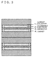
- F I G. 3 is a sectional view of conventional electric double layer capacitor used as a comparison example.
- the electric double layer capacitor device is so configured that two basic cell units are laminated.
- the current collector 1 (with a thickness of 100 ⁇ m) comprises electrically conductive rubber including carbon.
- the polarizable electrode 2 (with a thickness of 50 ⁇ m) comprises a porous sintered body obtained by sintering fine powder of activated carbon.
- the current collector 1 is laminated on the polarizable electrode 2 on the outer side of which a gasket 4 is disposed.
- This gasket 4 is provided in order to maintain the shape of the polarizable electrode 2 when the current collector 1 is placed opposite to the polarizable electrode 2 with a separator 3 (with a thickness of 25 ⁇ m) being interposed therebetween.
- a current collector 1 carbon is added to butyl rubber and the mixture is stirred to form a sheet-shaped film. Fine powder of activated carbon is sintered at a high temperature to produce a polarizable electrode 2. Then, the obtained current collector sheet and the polarizable electrode are cut to form a specified shape, respectively.
- the current collector 1 made up of butyl rubber and the gasket 4 are united by vulcanization to complete an electric double layer capacitor basic cell unit.
- the thickness of the conventional electric double layer capacitor device was 650 ⁇ m.
- the internal resistance was 200 m ⁇ .
- Table 1 is a list of the thickness and the internal resistance of the device shown in above embodiments 1 and 2 and in the comparison example.
- the internal resistance of the electric double layer capacitor shown in the above embodiments 1 and 2 is smaller and the capacitor has succeeded in achieving the thinness of the product.
- the present invention has the effect of implementing an electric double layer capacitor having smaller internal resistance compared with the conventional electric double layer capacitor.
- the contact area between the current collector and polarizable electrodes is surrounding the side of the polorizable electrode and the thermoplastic resins serving as binders are mutually compatirilized which induces the integration of the current collector and polarizable electrode, with a reduced contact resistance.
- the present invention has another effect of reducing the above-described internal resistance and of achieving the thicknness of the product.
- the capacitor is so configured that the integrated current collector and polarizable electrode have their abutting surfaces to the separator on the same flat plane. Namely, the starting polarizable electrode sheet is compressed to fill and form a rim protrusion 2b surrounding the lateral side of the polarizable electrode.
Landscapes
- Engineering & Computer Science (AREA)
- Power Engineering (AREA)
- Microelectronics & Electronic Packaging (AREA)
- Chemical & Material Sciences (AREA)
- Materials Engineering (AREA)
- Electric Double-Layer Capacitors Or The Like (AREA)
Applications Claiming Priority (3)
| Application Number | Priority Date | Filing Date | Title |
|---|---|---|---|
| JP9094612A JP2947215B2 (ja) | 1997-03-28 | 1997-03-28 | 電気二重層コンデンサ及びその製造方法 |
| JP94612/97 | 1997-03-28 | ||
| JP9461297 | 1997-03-28 |
Publications (3)
| Publication Number | Publication Date |
|---|---|
| EP0867902A2 true EP0867902A2 (fr) | 1998-09-30 |
| EP0867902A3 EP0867902A3 (fr) | 2002-05-15 |
| EP0867902B1 EP0867902B1 (fr) | 2006-05-17 |
Family
ID=14115079
Family Applications (1)
| Application Number | Title | Priority Date | Filing Date |
|---|---|---|---|
| EP98105632A Expired - Lifetime EP0867902B1 (fr) | 1997-03-28 | 1998-03-27 | Condensateur électrique à double couche et son procédé de fabrication |
Country Status (4)
| Country | Link |
|---|---|
| US (1) | US6064561A (fr) |
| EP (1) | EP0867902B1 (fr) |
| JP (1) | JP2947215B2 (fr) |
| DE (1) | DE69834520T2 (fr) |
Cited By (4)
| Publication number | Priority date | Publication date | Assignee | Title |
|---|---|---|---|---|
| CN100343930C (zh) * | 1999-01-19 | 2007-10-17 | 通用资源股份公司 | 带双电层的电容器 |
| FR2977364A1 (fr) * | 2011-07-01 | 2013-01-04 | Hutchinson | Collecteur de courant et procede de fabrication correspondant |
| WO2014168274A1 (fr) * | 2013-04-11 | 2014-10-16 | 주식회사 아모텍 | Supercondensateur et son procédé de fabrication |
| US9905332B2 (en) | 2012-10-03 | 2018-02-27 | Hutchinson | Transparent conductive electrode and associated production method |
Families Citing this family (19)
| Publication number | Priority date | Publication date | Assignee | Title |
|---|---|---|---|---|
| AU7240898A (en) * | 1997-12-18 | 1999-07-05 | Antares High Tek C.A. | Capacitor with dual electric layer |
| EP1026708B1 (fr) * | 1999-02-05 | 2007-12-19 | Kureha Corporation | Composition pour la formation d'électrodes, électrode en charbon actif et condensateur électrique à double couche |
| JP2001076971A (ja) * | 1999-09-03 | 2001-03-23 | Nec Corp | 電気二重層コンデンサおよびその製造方法 |
| TW505934B (en) | 2001-02-01 | 2002-10-11 | Luxon Energy Devices Corp | Manufacture method of electrochemical capacitor |
| US6917094B2 (en) * | 2002-11-29 | 2005-07-12 | Honda Motor Co., Ltd | Electrode for electric double layer capacitor |
| WO2005055259A1 (fr) * | 2003-12-03 | 2005-06-16 | Matsushita Electric Industrial Co., Ltd. | Accumulateur en forme de pièce de monnaie |
| US20050231893A1 (en) * | 2004-04-19 | 2005-10-20 | Harvey Troy A | Electric double layer capacitor enclosed in polymer housing |
| WO2006068291A1 (fr) * | 2004-12-21 | 2006-06-29 | Teijin Limited | Condensateur electrique double couche |
| RU2381586C2 (ru) | 2005-06-24 | 2010-02-10 | ЮНИВЕРСАЛ СУПЕРКАПАСИТОРЗ ЭлЭлСи | Электрод и коллектор тока для электрохимического конденсатора с двойным электрическим слоем и формируемый с ними электрохимический конденсатор с двойным электрическим слоем |
| JP2008544544A (ja) * | 2005-06-24 | 2008-12-04 | ユニバーサル・スーパーキャパシターズ・エルエルシー | 電気二重層電気化学キャパシタの集電体及び該集電体の製造方法 |
| EP1897104A1 (fr) | 2005-06-24 | 2008-03-12 | Universal Supercapacitors Llc. | Supracondensateur électrochimique hétérogène et procédé de fabrication |
| US7919014B2 (en) | 2006-11-27 | 2011-04-05 | Universal Supercapacitors Llc | Electrode for use with double electric layer electrochemical capacitors having high specific parameters |
| JP2014143226A (ja) * | 2013-01-22 | 2014-08-07 | Murata Mfg Co Ltd | フラッシュssd |
| US10312028B2 (en) | 2014-06-30 | 2019-06-04 | Avx Corporation | Electrochemical energy storage devices and manufacturing methods |
| GB2530576B (en) * | 2014-09-29 | 2019-12-25 | Univ Tartu | Method of forming a dielectric layer on an electrode |
| CN109155202B (zh) | 2016-05-20 | 2021-03-09 | 阿维科斯公司 | 多电池超级电容器 |
| CN109155204B (zh) | 2016-05-20 | 2020-12-22 | 阿维科斯公司 | 用于超级电容器的电极构造体 |
| MY194849A (en) | 2016-05-20 | 2022-12-19 | Kyocera Avx Components Corp | Ultracapacitor for use at high temperatures |
| US11830672B2 (en) | 2016-11-23 | 2023-11-28 | KYOCERA AVX Components Corporation | Ultracapacitor for use in a solder reflow process |
Family Cites Families (14)
| Publication number | Priority date | Publication date | Assignee | Title |
|---|---|---|---|---|
| US4626964A (en) * | 1984-03-19 | 1986-12-02 | Hitachi Maxell, Ltd. | Electrical double layer capacitor and production of the same |
| US4748542A (en) * | 1985-05-20 | 1988-05-31 | The Mead Corporation | Solid state electrochemical device |
| FR2583916B1 (fr) * | 1985-06-25 | 1990-01-12 | Europ Composants Electron | Cellule pour condensateur a double couche electrique et procede de fabrication d'une telle cellule |
| US4633372A (en) * | 1985-08-26 | 1986-12-30 | The Standard Oil Company | Polyoxometalate-modified carbon electrodes and uses therefor in capacitors |
| EP0230907A3 (fr) * | 1986-01-17 | 1989-05-31 | Asahi Glass Company Ltd. | Condensateur électrique à double couche à haute capacité |
| JPS6381914A (ja) * | 1986-09-26 | 1988-04-12 | 旭硝子株式会社 | 電気二重層コンデンサ |
| JP3093773B2 (ja) * | 1990-03-30 | 2000-10-03 | いすゞ自動車株式会社 | 電気二重層コンデンサおよびその製造方法 |
| JPH03283521A (ja) * | 1990-03-30 | 1991-12-13 | Isuzu Motors Ltd | 電気二重層コンデンサの製造方法 |
| JPH0582396A (ja) * | 1991-09-24 | 1993-04-02 | Isuzu Motors Ltd | 電気二重層コンデンサの製造方法 |
| US5381303A (en) * | 1992-05-20 | 1995-01-10 | Matsushita Electric Industrial Co., Ltd. | Electric double layer capacitor and method for manufacture thereof |
| JPH0684701A (ja) * | 1992-09-07 | 1994-03-25 | Matsushita Electric Ind Co Ltd | 電気二重層キャパシタおよびその製造方法 |
| RU2036523C1 (ru) * | 1992-07-03 | 1995-05-27 | Многопрофильное научно-техническое и производственно-коммерческое общество с ограниченной ответственностью "Эконд" | Конденсатор с двойным электрическим слоем |
| US5381323A (en) * | 1993-10-01 | 1995-01-10 | Regent Lighting Corporation | Sensor housing and adjustable mast arm for a swivel lighting fixture |
| JP3028056B2 (ja) * | 1996-02-19 | 2000-04-04 | 日本電気株式会社 | 電気二重層コンデンサ基本セルおよび電気二重層コンデンサ |
-
1997
- 1997-03-28 JP JP9094612A patent/JP2947215B2/ja not_active Expired - Fee Related
-
1998
- 1998-03-27 EP EP98105632A patent/EP0867902B1/fr not_active Expired - Lifetime
- 1998-03-27 US US09/050,637 patent/US6064561A/en not_active Expired - Fee Related
- 1998-03-27 DE DE69834520T patent/DE69834520T2/de not_active Expired - Fee Related
Cited By (8)
| Publication number | Priority date | Publication date | Assignee | Title |
|---|---|---|---|---|
| CN100343930C (zh) * | 1999-01-19 | 2007-10-17 | 通用资源股份公司 | 带双电层的电容器 |
| FR2977364A1 (fr) * | 2011-07-01 | 2013-01-04 | Hutchinson | Collecteur de courant et procede de fabrication correspondant |
| WO2013004666A1 (fr) * | 2011-07-01 | 2013-01-10 | Hutchinson | Électrode conductrice de courant et procede de fabrication correspondant |
| CN103748648A (zh) * | 2011-07-01 | 2014-04-23 | 哈钦森公司 | 导电电极以及相应的制造方法 |
| US9384907B2 (en) | 2011-07-01 | 2016-07-05 | Hutchinson | Current-conducting electrode and corresponding manufacturing process |
| CN103748648B (zh) * | 2011-07-01 | 2016-12-14 | 哈钦森公司 | 导电电极以及相应的制造方法 |
| US9905332B2 (en) | 2012-10-03 | 2018-02-27 | Hutchinson | Transparent conductive electrode and associated production method |
| WO2014168274A1 (fr) * | 2013-04-11 | 2014-10-16 | 주식회사 아모텍 | Supercondensateur et son procédé de fabrication |
Also Published As
| Publication number | Publication date |
|---|---|
| US6064561A (en) | 2000-05-16 |
| DE69834520D1 (de) | 2006-06-22 |
| EP0867902B1 (fr) | 2006-05-17 |
| JPH10275750A (ja) | 1998-10-13 |
| JP2947215B2 (ja) | 1999-09-13 |
| EP0867902A3 (fr) | 2002-05-15 |
| DE69834520T2 (de) | 2007-05-03 |
Similar Documents
| Publication | Publication Date | Title |
|---|---|---|
| EP0867902B1 (fr) | Condensateur électrique à double couche et son procédé de fabrication | |
| US6843810B2 (en) | Electric double layer capacitor and method for preparing the same | |
| US6391069B1 (en) | Method of making bonded-electrode rechargeable electrochemical cells | |
| US20110162198A1 (en) | Method of producing solid electrolyte-electrode assembly | |
| JP2000503161A (ja) | 積層状の再充電可能なバッテリセルを作成するための装置および方法 | |
| CN110739491B (zh) | 一种用涂胶隔膜制作软包锂电池的制作方法 | |
| JP2022144855A (ja) | 全固体電池及び全固体電池の製造方法 | |
| RU2005121126A (ru) | Композиционный материал и токоприемник для аккумуляторной батареи | |
| CN115312977B (zh) | 卷绕电芯及其制备方法、电池模组、电池包和用电设备 | |
| CN114927741B (zh) | 电芯热压装置和电芯 | |
| JP3436189B2 (ja) | 電気二重層コンデンサおよびその製造方法 | |
| JP2011527838A (ja) | 電極デバイス | |
| JPH0878028A (ja) | 固体高分子電解質燃料電池およびその製造方法 | |
| CA2632134A1 (fr) | Procede de fabrication d'ensemble electrode a membrane et membrane electrolytique renforcee dans une pile a combustible electrolytique polymere, et ensemble electrode a membrane et membrane electrolytique renforcee obtenues par | |
| JP4507412B2 (ja) | 積層セラミック電子部品の製造方法 | |
| JP2000286165A (ja) | 電気二重層コンデンサおよびその製造方法 | |
| JP2000277393A (ja) | 電気二重層コンデンサ及びその製造方法 | |
| JPH0684701A (ja) | 電気二重層キャパシタおよびその製造方法 | |
| CN218996759U (zh) | 一种裸电芯及电池 | |
| CN222214400U (zh) | 隔膜、电芯及热压工装 | |
| JPH02253569A (ja) | 固体二次電池の製造法 | |
| JP2002064038A (ja) | 電気二重層コンデンサ | |
| JPH03283518A (ja) | 電気二重層コンデンサおよびその製造方法 | |
| KR20230064201A (ko) | 핫프레싱 장치 | |
| JP2504467B2 (ja) | 溶融炭酸塩型燃料電池用電解質板及びその製造方法 |
Legal Events
| Date | Code | Title | Description |
|---|---|---|---|
| PUAI | Public reference made under article 153(3) epc to a published international application that has entered the european phase |
Free format text: ORIGINAL CODE: 0009012 |
|
| AK | Designated contracting states |
Kind code of ref document: A2 Designated state(s): AT BE CH DE DK ES FI FR GB GR IE IT LI LU MC NL PT SE |
|
| AX | Request for extension of the european patent |
Free format text: AL;LT;LV;MK;RO;SI |
|
| PUAL | Search report despatched |
Free format text: ORIGINAL CODE: 0009013 |
|
| RIC1 | Information provided on ipc code assigned before grant |
Free format text: 7H 01G 9/155 A, 7H 01G 9/00 B |
|
| AK | Designated contracting states |
Kind code of ref document: A3 Designated state(s): AT BE CH DE DK ES FI FR GB GR IE IT LI LU MC NL PT SE |
|
| AX | Request for extension of the european patent |
Free format text: AL;LT;LV;MK;RO;SI |
|
| 17P | Request for examination filed |
Effective date: 20020424 |
|
| RAP1 | Party data changed (applicant data changed or rights of an application transferred) |
Owner name: NEC TOKIN CORPORATION |
|
| 17Q | First examination report despatched |
Effective date: 20020923 |
|
| AKX | Designation fees paid |
Designated state(s): DE FR GB |
|
| GRAP | Despatch of communication of intention to grant a patent |
Free format text: ORIGINAL CODE: EPIDOSNIGR1 |
|
| GRAS | Grant fee paid |
Free format text: ORIGINAL CODE: EPIDOSNIGR3 |
|
| GRAA | (expected) grant |
Free format text: ORIGINAL CODE: 0009210 |
|
| AK | Designated contracting states |
Kind code of ref document: B1 Designated state(s): DE FR GB |
|
| REG | Reference to a national code |
Ref country code: GB Ref legal event code: FG4D |
|
| REF | Corresponds to: |
Ref document number: 69834520 Country of ref document: DE Date of ref document: 20060622 Kind code of ref document: P |
|
| PGFP | Annual fee paid to national office [announced via postgrant information from national office to epo] |
Ref country code: DE Payment date: 20070322 Year of fee payment: 10 |
|
| PLBE | No opposition filed within time limit |
Free format text: ORIGINAL CODE: 0009261 |
|
| STAA | Information on the status of an ep patent application or granted ep patent |
Free format text: STATUS: NO OPPOSITION FILED WITHIN TIME LIMIT |
|
| 26N | No opposition filed |
Effective date: 20070220 |
|
| EN | Fr: translation not filed | ||
| GBPC | Gb: european patent ceased through non-payment of renewal fee |
Effective date: 20070327 |
|
| PG25 | Lapsed in a contracting state [announced via postgrant information from national office to epo] |
Ref country code: GB Free format text: LAPSE BECAUSE OF NON-PAYMENT OF DUE FEES Effective date: 20070327 Ref country code: FR Free format text: LAPSE BECAUSE OF FAILURE TO SUBMIT A TRANSLATION OF THE DESCRIPTION OR TO PAY THE FEE WITHIN THE PRESCRIBED TIME-LIMIT Effective date: 20070309 |
|
| PG25 | Lapsed in a contracting state [announced via postgrant information from national office to epo] |
Ref country code: FR Free format text: LAPSE BECAUSE OF FAILURE TO SUBMIT A TRANSLATION OF THE DESCRIPTION OR TO PAY THE FEE WITHIN THE PRESCRIBED TIME-LIMIT Effective date: 20060517 |
|
| PG25 | Lapsed in a contracting state [announced via postgrant information from national office to epo] |
Ref country code: DE Free format text: LAPSE BECAUSE OF NON-PAYMENT OF DUE FEES Effective date: 20081001 |