EP0867923A2 - Verfahren zur Herstellung einer dünnen Schicht - Google Patents
Verfahren zur Herstellung einer dünnen Schicht Download PDFInfo
- Publication number
- EP0867923A2 EP0867923A2 EP98302218A EP98302218A EP0867923A2 EP 0867923 A2 EP0867923 A2 EP 0867923A2 EP 98302218 A EP98302218 A EP 98302218A EP 98302218 A EP98302218 A EP 98302218A EP 0867923 A2 EP0867923 A2 EP 0867923A2
- Authority
- EP
- European Patent Office
- Prior art keywords
- layer
- wire
- substrate
- porous
- porosity
- Prior art date
- Legal status (The legal status is an assumption and is not a legal conclusion. Google has not performed a legal analysis and makes no representation as to the accuracy of the status listed.)
- Granted
Links
Images









Classifications
-
- B—PERFORMING OPERATIONS; TRANSPORTING
- B32—LAYERED PRODUCTS
- B32B—LAYERED PRODUCTS, i.e. PRODUCTS BUILT-UP OF STRATA OF FLAT OR NON-FLAT, e.g. CELLULAR OR HONEYCOMB, FORM
- B32B43/00—Operations specially adapted for layered products and not otherwise provided for, e.g. repairing; Apparatus therefor
-
- H—ELECTRICITY
- H10—SEMICONDUCTOR DEVICES; ELECTRIC SOLID-STATE DEVICES NOT OTHERWISE PROVIDED FOR
- H10F—INORGANIC SEMICONDUCTOR DEVICES SENSITIVE TO INFRARED RADIATION, LIGHT, ELECTROMAGNETIC RADIATION OF SHORTER WAVELENGTH OR CORPUSCULAR RADIATION
- H10F99/00—Subject matter not provided for in other groups of this subclass
-
- H—ELECTRICITY
- H10—SEMICONDUCTOR DEVICES; ELECTRIC SOLID-STATE DEVICES NOT OTHERWISE PROVIDED FOR
- H10P—GENERIC PROCESSES OR APPARATUS FOR THE MANUFACTURE OR TREATMENT OF DEVICES COVERED BY CLASS H10
- H10P90/00—Preparation of wafers not covered by a single main group of this subclass, e.g. wafer reinforcement
- H10P90/19—Preparing inhomogeneous wafers
- H10P90/1904—Preparing vertically inhomogeneous wafers
- H10P90/1906—Preparing SOI wafers
- H10P90/1914—Preparing SOI wafers using bonding
-
- H—ELECTRICITY
- H10—SEMICONDUCTOR DEVICES; ELECTRIC SOLID-STATE DEVICES NOT OTHERWISE PROVIDED FOR
- H10P—GENERIC PROCESSES OR APPARATUS FOR THE MANUFACTURE OR TREATMENT OF DEVICES COVERED BY CLASS H10
- H10P90/00—Preparation of wafers not covered by a single main group of this subclass, e.g. wafer reinforcement
- H10P90/19—Preparing inhomogeneous wafers
- H10P90/1904—Preparing vertically inhomogeneous wafers
- H10P90/1906—Preparing SOI wafers
- H10P90/1924—Preparing SOI wafers with separation/delamination along a porous layer
-
- H—ELECTRICITY
- H10—SEMICONDUCTOR DEVICES; ELECTRIC SOLID-STATE DEVICES NOT OTHERWISE PROVIDED FOR
- H10W—GENERIC PACKAGES, INTERCONNECTIONS, CONNECTORS OR OTHER CONSTRUCTIONAL DETAILS OF DEVICES COVERED BY CLASS H10
- H10W10/00—Isolation regions in semiconductor bodies between components of integrated devices
- H10W10/10—Isolation regions comprising dielectric materials
- H10W10/181—Semiconductor-on-insulator [SOI] isolation regions, e.g. buried oxide regions of SOI wafers
-
- Y—GENERAL TAGGING OF NEW TECHNOLOGICAL DEVELOPMENTS; GENERAL TAGGING OF CROSS-SECTIONAL TECHNOLOGIES SPANNING OVER SEVERAL SECTIONS OF THE IPC; TECHNICAL SUBJECTS COVERED BY FORMER USPC CROSS-REFERENCE ART COLLECTIONS [XRACs] AND DIGESTS
- Y10—TECHNICAL SUBJECTS COVERED BY FORMER USPC
- Y10S—TECHNICAL SUBJECTS COVERED BY FORMER USPC CROSS-REFERENCE ART COLLECTIONS [XRACs] AND DIGESTS
- Y10S438/00—Semiconductor device manufacturing: process
- Y10S438/96—Porous semiconductor
-
- Y—GENERAL TAGGING OF NEW TECHNOLOGICAL DEVELOPMENTS; GENERAL TAGGING OF CROSS-SECTIONAL TECHNOLOGIES SPANNING OVER SEVERAL SECTIONS OF THE IPC; TECHNICAL SUBJECTS COVERED BY FORMER USPC CROSS-REFERENCE ART COLLECTIONS [XRACs] AND DIGESTS
- Y10—TECHNICAL SUBJECTS COVERED BY FORMER USPC
- Y10S—TECHNICAL SUBJECTS COVERED BY FORMER USPC CROSS-REFERENCE ART COLLECTIONS [XRACs] AND DIGESTS
- Y10S438/00—Semiconductor device manufacturing: process
- Y10S438/974—Substrate surface preparation
-
- Y—GENERAL TAGGING OF NEW TECHNOLOGICAL DEVELOPMENTS; GENERAL TAGGING OF CROSS-SECTIONAL TECHNOLOGIES SPANNING OVER SEVERAL SECTIONS OF THE IPC; TECHNICAL SUBJECTS COVERED BY FORMER USPC CROSS-REFERENCE ART COLLECTIONS [XRACs] AND DIGESTS
- Y10—TECHNICAL SUBJECTS COVERED BY FORMER USPC
- Y10S—TECHNICAL SUBJECTS COVERED BY FORMER USPC CROSS-REFERENCE ART COLLECTIONS [XRACs] AND DIGESTS
- Y10S438/00—Semiconductor device manufacturing: process
- Y10S438/977—Thinning or removal of substrate
Definitions
- the first to eighth embodiments show modes of producing an SOI substrate
- the ninth to eleventh embodiments show modes of producing a photoelectric conversion unit such as a solar cell or an area sensor.
- the twelfth embodiment shows use of hydrogen ions.
- the present invention is not limited by or to only the respective embodiments, and also includes modes of combining the respective embodiments.
- the porous Si layer 3 When the porous Si layer 3 is formed in a sufficiently small thickness during the anodization process, the porous Si layer 3 substantially remains on neither of the substrates after the separation.
- FIGS. 10A and 10B are a perspective view of a substrate showing a separating process of the third embodiment, and a cross-sectional view of the substrate, respectively.
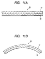
- reference numeral 35 denotes a wire that forms a bimetal
- 36 a support bar that supports the bimetal 35
- 37 a brass that forms a bimetal 35 and is large in thermal expansion coefficient
- 38 an invar that forms the bimetal 35 and is small in thermal expansion coefficient.
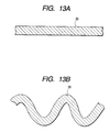
- FIG. 11A shows the shape of the bimetal 35 at a room temperature
- FIG. 11B shows the shape of the bimetal 35 when heated. When heated, the bimetal 35 is warped as shown in FIG. 11B because the brass 37 larger in thermal expansion coefficient will expand more than the invar 38 smaller in thermal expansion coefficient.
- the fourth embodiment is directed to a mode of producing an SOI substrate in which, in order that an article ATL is separated into an Si wafer to be reused and an SOI substrate at a porous Si layer, a wire made of a shape-memory alloy is used. Then, the wire made of a shape-memory alloy is cooled to be contracted to conduct the separation of the substrate.
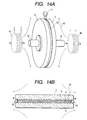
- FIGS. 15A and 15B are views showing a separating process of the sixth embodiment, in which FIG. 15A is a perspective view of the substrate, and FIG. 15B is a cross-sectional view of the substrate, respectively.
- reference numeral 44 denotes a chuck that supports the Si wafer 6 and also supports a conductor 46 that constitutes an electromagnet; 45, a center axis of the conductor 46 that constitutes the electromagnet; 47, lines of magnetic force of a static magnetic field developed by the electromagnet 46; and 42 is a conductor that receives the Lorentz's force from the static magnetic field which is a wire of the present invention.
- Reference numeral 48 denotes a d.c.
- the eighth embodiment is directed to a mode of producing an SOI substrate in which, in order that an article ATC is separated into an Si wafer to be reused and an SOI substrate at a porous Si layer, a wire wound around a substrate is merely tightened up to give a separation force to the substrate.
- the wire may be heated by supplying a current to the wire.
Landscapes
- Recrystallisation Techniques (AREA)
- Photovoltaic Devices (AREA)
- Separation Using Semi-Permeable Membranes (AREA)
- Mechanical Treatment Of Semiconductor (AREA)
- Crystals, And After-Treatments Of Crystals (AREA)
Applications Claiming Priority (3)
| Application Number | Priority Date | Filing Date | Title |
|---|---|---|---|
| JP7377097 | 1997-03-26 | ||
| JP7377097 | 1997-03-26 | ||
| JP73770/97 | 1997-03-26 |
Publications (3)
| Publication Number | Publication Date |
|---|---|
| EP0867923A2 true EP0867923A2 (de) | 1998-09-30 |
| EP0867923A3 EP0867923A3 (de) | 1999-07-28 |
| EP0867923B1 EP0867923B1 (de) | 2004-06-23 |
Family
ID=13527788
Family Applications (1)
| Application Number | Title | Priority Date | Filing Date |
|---|---|---|---|
| EP98302218A Expired - Lifetime EP0867923B1 (de) | 1997-03-26 | 1998-03-24 | Verfahren zur Trennung einer Schicht |
Country Status (8)
| Country | Link |
|---|---|
| US (1) | US6140209A (de) |
| EP (1) | EP0867923B1 (de) |
| KR (1) | KR100266954B1 (de) |
| AT (1) | ATE270001T1 (de) |
| AU (1) | AU744858B2 (de) |
| CA (1) | CA2232796C (de) |
| DE (1) | DE69824655T2 (de) |
| TW (1) | TW389958B (de) |
Families Citing this family (36)
| Publication number | Priority date | Publication date | Assignee | Title |
|---|---|---|---|---|
| US7148119B1 (en) * | 1994-03-10 | 2006-12-12 | Canon Kabushiki Kaisha | Process for production of semiconductor substrate |
| US6306729B1 (en) | 1997-12-26 | 2001-10-23 | Canon Kabushiki Kaisha | Semiconductor article and method of manufacturing the same |
| FR2785217B1 (fr) * | 1998-10-30 | 2001-01-19 | Soitec Silicon On Insulator | Procede et dispositif pour separer en deux tranches une plaque de materiau notamment semi-conducteur |
| JP2000223683A (ja) * | 1999-02-02 | 2000-08-11 | Canon Inc | 複合部材及びその分離方法、貼り合わせ基板及びその分離方法、移設層の移設方法、並びにsoi基板の製造方法 |
| FR2796491B1 (fr) * | 1999-07-12 | 2001-08-31 | Commissariat Energie Atomique | Procede de decollement de deux elements et dispositif pour sa mise en oeuvre |
| JP3948930B2 (ja) * | 2001-10-31 | 2007-07-25 | 大日本スクリーン製造株式会社 | 薄膜形成装置および薄膜形成方法 |
| US7452757B2 (en) * | 2002-05-07 | 2008-11-18 | Asm America, Inc. | Silicon-on-insulator structures and methods |
| JP2004140120A (ja) * | 2002-10-16 | 2004-05-13 | Canon Inc | 多結晶シリコン基板 |
| US7176528B2 (en) * | 2003-02-18 | 2007-02-13 | Corning Incorporated | Glass-based SOI structures |
| US7399681B2 (en) | 2003-02-18 | 2008-07-15 | Corning Incorporated | Glass-based SOI structures |
| KR20060017771A (ko) * | 2003-05-06 | 2006-02-27 | 캐논 가부시끼가이샤 | 반도체기판, 반도체디바이스, 발광다이오드 및 그 제조방법 |
| JP2004335642A (ja) * | 2003-05-06 | 2004-11-25 | Canon Inc | 基板およびその製造方法 |
| US20050124137A1 (en) * | 2003-05-07 | 2005-06-09 | Canon Kabushiki Kaisha | Semiconductor substrate and manufacturing method therefor |
| JP2005005509A (ja) * | 2003-06-12 | 2005-01-06 | Canon Inc | 薄膜トランジスタ及びその製造方法 |
| US20050082526A1 (en) * | 2003-10-15 | 2005-04-21 | International Business Machines Corporation | Techniques for layer transfer processing |
| JP2005135942A (ja) * | 2003-10-28 | 2005-05-26 | Canon Inc | 電極配設方法 |
| JP4771510B2 (ja) * | 2004-06-23 | 2011-09-14 | キヤノン株式会社 | 半導体層の製造方法及び基板の製造方法 |
| WO2006012544A2 (en) * | 2004-07-22 | 2006-02-02 | The Board Of Trustees Of The Leland Stanford Junior University | Germanium substrate-type materials and approach therefor |
| CN100527416C (zh) * | 2004-08-18 | 2009-08-12 | 康宁股份有限公司 | 应变绝缘体上半导体结构以及应变绝缘体上半导体结构的制造方法 |
| CN101091251B (zh) * | 2004-08-18 | 2011-03-16 | 康宁股份有限公司 | 包含高应变玻璃或玻璃陶瓷的绝缘体上半导体结构 |
| US7268051B2 (en) * | 2005-08-26 | 2007-09-11 | Corning Incorporated | Semiconductor on glass insulator with deposited barrier layer |
| DE102005047509B4 (de) * | 2005-10-04 | 2017-10-26 | Degotec Gmbh | Vorrichtung zur Separierung eines flächigen Objektes von einem Körper, mit dem das Objekt mittels Adhäsionskraft verbunden ist |
| US7691730B2 (en) * | 2005-11-22 | 2010-04-06 | Corning Incorporated | Large area semiconductor on glass insulator |
| US20070264796A1 (en) * | 2006-05-12 | 2007-11-15 | Stocker Mark A | Method for forming a semiconductor on insulator structure |
| JP5171016B2 (ja) * | 2006-10-27 | 2013-03-27 | キヤノン株式会社 | 半導体部材、半導体物品の製造方法、その製造方法を用いたledアレイ |
| US20080277778A1 (en) | 2007-05-10 | 2008-11-13 | Furman Bruce K | Layer Transfer Process and Functionally Enhanced Integrated Circuits Products Thereby |
| JP2009094144A (ja) * | 2007-10-04 | 2009-04-30 | Canon Inc | 発光素子の製造方法 |
| DE102007050483A1 (de) | 2007-10-19 | 2009-09-10 | Meyer Burger Ag | Mischung aus einem thixotropen Dispersionsmedium sowie abrasiv wirkenden Körnern als Schleifmittel |
| US8950459B2 (en) | 2009-04-16 | 2015-02-10 | Suss Microtec Lithography Gmbh | Debonding temporarily bonded semiconductor wafers |
| US8366873B2 (en) * | 2010-04-15 | 2013-02-05 | Suss Microtec Lithography, Gmbh | Debonding equipment and methods for debonding temporary bonded wafers |
| US8764026B2 (en) * | 2009-04-16 | 2014-07-01 | Suss Microtec Lithography, Gmbh | Device for centering wafers |
| US8592294B2 (en) * | 2010-02-22 | 2013-11-26 | Asm International N.V. | High temperature atomic layer deposition of dielectric oxides |
| US9755015B1 (en) | 2016-05-10 | 2017-09-05 | Globalfoundries Inc. | Air gaps formed by porous silicon removal |
| CN108242424B (zh) | 2016-12-26 | 2019-09-03 | 京东方科技集团股份有限公司 | 柔性面板的制作方法、柔性面板及显示装置 |
| WO2020078559A1 (en) * | 2018-10-18 | 2020-04-23 | Applied Materials, Inc. | Holding device for holding a substrate, carrier for holding a substrate, and method for releasing a substrate from a holding device |
| CN111855636B (zh) * | 2019-04-29 | 2023-10-27 | 中国科学院微电子研究所 | 一种sers基底 |
Family Cites Families (7)
| Publication number | Priority date | Publication date | Assignee | Title |
|---|---|---|---|---|
| US4445965A (en) * | 1980-12-01 | 1984-05-01 | Carnegie-Mellon University | Method for making thin film cadmium telluride and related semiconductors for solar cells |
| JPH01156480A (ja) * | 1987-12-14 | 1989-06-20 | Somar Corp | 薄膜剥離装置 |
| SG59963A1 (en) * | 1990-08-03 | 1999-02-22 | Canon Kk | Semiconductor member and process for preparing semiconductor member |
| FR2681472B1 (fr) * | 1991-09-18 | 1993-10-29 | Commissariat Energie Atomique | Procede de fabrication de films minces de materiau semiconducteur. |
| JP3257580B2 (ja) * | 1994-03-10 | 2002-02-18 | キヤノン株式会社 | 半導体基板の作製方法 |
| JP3381443B2 (ja) * | 1995-02-02 | 2003-02-24 | ソニー株式会社 | 基体から半導体層を分離する方法、半導体素子の製造方法およびsoi基板の製造方法 |
| EP0757377B1 (de) * | 1995-08-02 | 2003-04-09 | Canon Kabushiki Kaisha | Halbleitersubstrat und Herstellungsverfahren |
-
1998
- 1998-03-20 CA CA002232796A patent/CA2232796C/en not_active Expired - Fee Related
- 1998-03-23 US US09/045,955 patent/US6140209A/en not_active Expired - Fee Related
- 1998-03-23 TW TW087104312A patent/TW389958B/zh not_active IP Right Cessation
- 1998-03-24 AT AT98302218T patent/ATE270001T1/de not_active IP Right Cessation
- 1998-03-24 DE DE69824655T patent/DE69824655T2/de not_active Expired - Fee Related
- 1998-03-24 KR KR1019980010066A patent/KR100266954B1/ko not_active Expired - Fee Related
- 1998-03-24 EP EP98302218A patent/EP0867923B1/de not_active Expired - Lifetime
- 1998-03-25 AU AU59523/98A patent/AU744858B2/en not_active Ceased
Also Published As
| Publication number | Publication date |
|---|---|
| EP0867923A3 (de) | 1999-07-28 |
| DE69824655T2 (de) | 2005-08-04 |
| AU5952398A (en) | 1998-10-01 |
| KR19980080586A (ko) | 1998-11-25 |
| CA2232796A1 (en) | 1998-09-26 |
| KR100266954B1 (ko) | 2000-10-02 |
| EP0867923B1 (de) | 2004-06-23 |
| ATE270001T1 (de) | 2004-07-15 |
| DE69824655D1 (de) | 2004-07-29 |
| US6140209A (en) | 2000-10-31 |
| TW389958B (en) | 2000-05-11 |
| CA2232796C (en) | 2002-01-22 |
| AU744858B2 (en) | 2002-03-07 |
Similar Documents
| Publication | Publication Date | Title |
|---|---|---|
| CA2232796C (en) | Thin film forming process | |
| KR100304161B1 (ko) | 반도체부재의제조방법 | |
| US6448155B1 (en) | Production method of semiconductor base material and production method of solar cell | |
| JP3962465B2 (ja) | 半導体部材の製造方法 | |
| KR100440853B1 (ko) | 박막 반도체, 태양전지 및 발광 다이오드의 제조 방법 | |
| US7022585B2 (en) | Method for making thin film devices intended for solar cells or silicon-on-insulator (SOI) applications | |
| AU744654B2 (en) | Substrate and production method thereof | |
| US9178105B2 (en) | Flexible monocrystalline thin silicon cell | |
| CA2233132C (en) | Semiconductor substrate and process for producing same | |
| JPH10233352A5 (de) | ||
| JP2001094136A (ja) | 半導体素子モジュールの製造方法および太陽電池モジュールの製造方法 | |
| WO2000045426A1 (en) | Method for fabricating thin film semiconductor devices | |
| JP3667079B2 (ja) | 薄膜の形成方法 | |
| JPH1079524A (ja) | 薄膜太陽電池の製造方法 | |
| JP4035862B2 (ja) | 半導体基板の製造方法 | |
| JP3927977B2 (ja) | 半導体部材の製造方法 | |
| JP2002343995A (ja) | 集積型薄膜素子およびその製造方法 | |
| CN1194452A (zh) | 薄膜形成工艺 | |
| JPH10326758A (ja) | 薄膜の形成方法 | |
| EP1385200B1 (de) | Verfahren zur Herstellung von Dünnschichtbauelementen für Solarzellen oder SOI-Anwendungen | |
| JPH11330518A (ja) | 薄膜半導体の分離方法、光電変換装置の製造方法および太陽電池 | |
| JP2001023953A (ja) | 半導体基体及びその製造方法 |
Legal Events
| Date | Code | Title | Description |
|---|---|---|---|
| PUAI | Public reference made under article 153(3) epc to a published international application that has entered the european phase |
Free format text: ORIGINAL CODE: 0009012 |
|
| AK | Designated contracting states |
Kind code of ref document: A2 Designated state(s): AT BE CH DE ES FR GB IT LI NL PT SE |
|
| AX | Request for extension of the european patent |
Free format text: AL;LT;LV;MK;RO;SI |
|
| PUAL | Search report despatched |
Free format text: ORIGINAL CODE: 0009013 |
|
| AK | Designated contracting states |
Kind code of ref document: A3 Designated state(s): AT BE CH DE DK ES FI FR GB GR IE IT LI LU MC NL PT SE |
|
| AX | Request for extension of the european patent |
Free format text: AL;LT;LV;MK;RO;SI |
|
| 17P | Request for examination filed |
Effective date: 19991210 |
|
| AKX | Designation fees paid |
Free format text: AT BE CH DE ES FR GB IT LI NL PT SE |
|
| 17Q | First examination report despatched |
Effective date: 20020222 |
|
| GRAP | Despatch of communication of intention to grant a patent |
Free format text: ORIGINAL CODE: EPIDOSNIGR1 |
|
| RTI1 | Title (correction) |
Free format text: PROCESS OF SEPARATING A LAYER |
|
| GRAS | Grant fee paid |
Free format text: ORIGINAL CODE: EPIDOSNIGR3 |
|
| GRAA | (expected) grant |
Free format text: ORIGINAL CODE: 0009210 |
|
| AK | Designated contracting states |
Kind code of ref document: B1 Designated state(s): AT BE CH DE ES FR GB IT LI NL PT SE |
|
| PG25 | Lapsed in a contracting state [announced via postgrant information from national office to epo] |
Ref country code: NL Free format text: LAPSE BECAUSE OF FAILURE TO SUBMIT A TRANSLATION OF THE DESCRIPTION OR TO PAY THE FEE WITHIN THE PRESCRIBED TIME-LIMIT Effective date: 20040623 Ref country code: LI Free format text: LAPSE BECAUSE OF FAILURE TO SUBMIT A TRANSLATION OF THE DESCRIPTION OR TO PAY THE FEE WITHIN THE PRESCRIBED TIME-LIMIT Effective date: 20040623 Ref country code: IT Free format text: LAPSE BECAUSE OF FAILURE TO SUBMIT A TRANSLATION OF THE DESCRIPTION OR TO PAY THE FEE WITHIN THE PRESCRIBED TIME-LIMIT;WARNING: LAPSES OF ITALIAN PATENTS WITH EFFECTIVE DATE BEFORE 2007 MAY HAVE OCCURRED AT ANY TIME BEFORE 2007. THE CORRECT EFFECTIVE DATE MAY BE DIFFERENT FROM THE ONE RECORDED. Effective date: 20040623 Ref country code: CH Free format text: LAPSE BECAUSE OF FAILURE TO SUBMIT A TRANSLATION OF THE DESCRIPTION OR TO PAY THE FEE WITHIN THE PRESCRIBED TIME-LIMIT Effective date: 20040623 Ref country code: BE Free format text: LAPSE BECAUSE OF FAILURE TO SUBMIT A TRANSLATION OF THE DESCRIPTION OR TO PAY THE FEE WITHIN THE PRESCRIBED TIME-LIMIT Effective date: 20040623 Ref country code: AT Free format text: LAPSE BECAUSE OF FAILURE TO SUBMIT A TRANSLATION OF THE DESCRIPTION OR TO PAY THE FEE WITHIN THE PRESCRIBED TIME-LIMIT Effective date: 20040623 |
|
| REG | Reference to a national code |
Ref country code: GB Ref legal event code: FG4D |
|
| REG | Reference to a national code |
Ref country code: CH Ref legal event code: EP |
|
| REF | Corresponds to: |
Ref document number: 69824655 Country of ref document: DE Date of ref document: 20040729 Kind code of ref document: P |
|
| PG25 | Lapsed in a contracting state [announced via postgrant information from national office to epo] |
Ref country code: SE Free format text: LAPSE BECAUSE OF FAILURE TO SUBMIT A TRANSLATION OF THE DESCRIPTION OR TO PAY THE FEE WITHIN THE PRESCRIBED TIME-LIMIT Effective date: 20040923 |
|
| PG25 | Lapsed in a contracting state [announced via postgrant information from national office to epo] |
Ref country code: ES Free format text: LAPSE BECAUSE OF FAILURE TO SUBMIT A TRANSLATION OF THE DESCRIPTION OR TO PAY THE FEE WITHIN THE PRESCRIBED TIME-LIMIT Effective date: 20041004 |
|
| NLV1 | Nl: lapsed or annulled due to failure to fulfill the requirements of art. 29p and 29m of the patents act | ||
| REG | Reference to a national code |
Ref country code: CH Ref legal event code: PL |
|
| ET | Fr: translation filed | ||
| PLBE | No opposition filed within time limit |
Free format text: ORIGINAL CODE: 0009261 |
|
| STAA | Information on the status of an ep patent application or granted ep patent |
Free format text: STATUS: NO OPPOSITION FILED WITHIN TIME LIMIT |
|
| 26N | No opposition filed |
Effective date: 20050324 |
|
| PG25 | Lapsed in a contracting state [announced via postgrant information from national office to epo] |
Ref country code: PT Free format text: LAPSE BECAUSE OF NON-PAYMENT OF DUE FEES Effective date: 20041123 |
|
| PGFP | Annual fee paid to national office [announced via postgrant information from national office to epo] |
Ref country code: GB Payment date: 20080326 Year of fee payment: 11 |
|
| PGFP | Annual fee paid to national office [announced via postgrant information from national office to epo] |
Ref country code: DE Payment date: 20080331 Year of fee payment: 11 |
|
| PGFP | Annual fee paid to national office [announced via postgrant information from national office to epo] |
Ref country code: FR Payment date: 20080321 Year of fee payment: 11 |
|
| GBPC | Gb: european patent ceased through non-payment of renewal fee |
Effective date: 20090324 |
|
| REG | Reference to a national code |
Ref country code: FR Ref legal event code: ST Effective date: 20091130 |
|
| PG25 | Lapsed in a contracting state [announced via postgrant information from national office to epo] |
Ref country code: DE Free format text: LAPSE BECAUSE OF NON-PAYMENT OF DUE FEES Effective date: 20091001 |
|
| PG25 | Lapsed in a contracting state [announced via postgrant information from national office to epo] |
Ref country code: GB Free format text: LAPSE BECAUSE OF NON-PAYMENT OF DUE FEES Effective date: 20090324 Ref country code: FR Free format text: LAPSE BECAUSE OF NON-PAYMENT OF DUE FEES Effective date: 20091123 |