EP0867932A2 - Verfahren zur Herstellung von Bonddrahtverbindungen - Google Patents
Verfahren zur Herstellung von Bonddrahtverbindungen Download PDFInfo
- Publication number
- EP0867932A2 EP0867932A2 EP97119991A EP97119991A EP0867932A2 EP 0867932 A2 EP0867932 A2 EP 0867932A2 EP 97119991 A EP97119991 A EP 97119991A EP 97119991 A EP97119991 A EP 97119991A EP 0867932 A2 EP0867932 A2 EP 0867932A2
- Authority
- EP
- European Patent Office
- Prior art keywords
- component
- conductor tracks
- bond
- connection
- connections
- Prior art date
- Legal status (The legal status is an assumption and is not a legal conclusion. Google has not performed a legal analysis and makes no representation as to the accuracy of the status listed.)
- Granted
Links
Images

Classifications
-
- H—ELECTRICITY
- H10—SEMICONDUCTOR DEVICES; ELECTRIC SOLID-STATE DEVICES NOT OTHERWISE PROVIDED FOR
- H10W—GENERIC PACKAGES, INTERCONNECTIONS, CONNECTORS OR OTHER CONSTRUCTIONAL DETAILS OF DEVICES COVERED BY CLASS H10
- H10W72/00—Interconnections or connectors in packages
- H10W72/90—Bond pads, in general
-
- H—ELECTRICITY
- H10—SEMICONDUCTOR DEVICES; ELECTRIC SOLID-STATE DEVICES NOT OTHERWISE PROVIDED FOR
- H10W—GENERIC PACKAGES, INTERCONNECTIONS, CONNECTORS OR OTHER CONSTRUCTIONAL DETAILS OF DEVICES COVERED BY CLASS H10
- H10W72/00—Interconnections or connectors in packages
- H10W72/071—Connecting or disconnecting
- H10W72/0711—Apparatus therefor
- H10W72/07141—Means for applying energy, e.g. ovens or lasers
-
- H—ELECTRICITY
- H10—SEMICONDUCTOR DEVICES; ELECTRIC SOLID-STATE DEVICES NOT OTHERWISE PROVIDED FOR
- H10W—GENERIC PACKAGES, INTERCONNECTIONS, CONNECTORS OR OTHER CONSTRUCTIONAL DETAILS OF DEVICES COVERED BY CLASS H10
- H10W72/00—Interconnections or connectors in packages
- H10W72/071—Connecting or disconnecting
- H10W72/075—Connecting or disconnecting of bond wires
- H10W72/07531—Techniques
- H10W72/07532—Compression bonding, e.g. thermocompression bonding
- H10W72/07533—Ultrasonic bonding, e.g. thermosonic bonding
-
- H—ELECTRICITY
- H10—SEMICONDUCTOR DEVICES; ELECTRIC SOLID-STATE DEVICES NOT OTHERWISE PROVIDED FOR
- H10W—GENERIC PACKAGES, INTERCONNECTIONS, CONNECTORS OR OTHER CONSTRUCTIONAL DETAILS OF DEVICES COVERED BY CLASS H10
- H10W72/00—Interconnections or connectors in packages
- H10W72/071—Connecting or disconnecting
- H10W72/075—Connecting or disconnecting of bond wires
- H10W72/07551—Connecting or disconnecting of bond wires characterised by changes in properties of the bond wires during the connecting
- H10W72/07554—Connecting or disconnecting of bond wires characterised by changes in properties of the bond wires during the connecting changes in dispositions
-
- H—ELECTRICITY
- H10—SEMICONDUCTOR DEVICES; ELECTRIC SOLID-STATE DEVICES NOT OTHERWISE PROVIDED FOR
- H10W—GENERIC PACKAGES, INTERCONNECTIONS, CONNECTORS OR OTHER CONSTRUCTIONAL DETAILS OF DEVICES COVERED BY CLASS H10
- H10W72/00—Interconnections or connectors in packages
- H10W72/50—Bond wires
- H10W72/531—Shapes of wire connectors
- H10W72/536—Shapes of wire connectors the connected ends being ball-shaped
-
- H—ELECTRICITY
- H10—SEMICONDUCTOR DEVICES; ELECTRIC SOLID-STATE DEVICES NOT OTHERWISE PROVIDED FOR
- H10W—GENERIC PACKAGES, INTERCONNECTIONS, CONNECTORS OR OTHER CONSTRUCTIONAL DETAILS OF DEVICES COVERED BY CLASS H10
- H10W72/00—Interconnections or connectors in packages
- H10W72/50—Bond wires
- H10W72/531—Shapes of wire connectors
- H10W72/5363—Shapes of wire connectors the connected ends being wedge-shaped
-
- H—ELECTRICITY
- H10—SEMICONDUCTOR DEVICES; ELECTRIC SOLID-STATE DEVICES NOT OTHERWISE PROVIDED FOR
- H10W—GENERIC PACKAGES, INTERCONNECTIONS, CONNECTORS OR OTHER CONSTRUCTIONAL DETAILS OF DEVICES COVERED BY CLASS H10
- H10W72/00—Interconnections or connectors in packages
- H10W72/50—Bond wires
- H10W72/541—Dispositions of bond wires
- H10W72/5445—Dispositions of bond wires being orthogonal to a side surface of the chip, e.g. parallel arrangements
-
- H—ELECTRICITY
- H10—SEMICONDUCTOR DEVICES; ELECTRIC SOLID-STATE DEVICES NOT OTHERWISE PROVIDED FOR
- H10W—GENERIC PACKAGES, INTERCONNECTIONS, CONNECTORS OR OTHER CONSTRUCTIONAL DETAILS OF DEVICES COVERED BY CLASS H10
- H10W72/00—Interconnections or connectors in packages
- H10W72/50—Bond wires
- H10W72/541—Dispositions of bond wires
- H10W72/5449—Dispositions of bond wires not being orthogonal to a side surface of the chip, e.g. fan-out arrangements
-
- H—ELECTRICITY
- H10—SEMICONDUCTOR DEVICES; ELECTRIC SOLID-STATE DEVICES NOT OTHERWISE PROVIDED FOR
- H10W—GENERIC PACKAGES, INTERCONNECTIONS, CONNECTORS OR OTHER CONSTRUCTIONAL DETAILS OF DEVICES COVERED BY CLASS H10
- H10W72/00—Interconnections or connectors in packages
- H10W72/50—Bond wires
- H10W72/541—Dispositions of bond wires
- H10W72/547—Dispositions of multiple bond wires
-
- H—ELECTRICITY
- H10—SEMICONDUCTOR DEVICES; ELECTRIC SOLID-STATE DEVICES NOT OTHERWISE PROVIDED FOR
- H10W—GENERIC PACKAGES, INTERCONNECTIONS, CONNECTORS OR OTHER CONSTRUCTIONAL DETAILS OF DEVICES COVERED BY CLASS H10
- H10W72/00—Interconnections or connectors in packages
- H10W72/50—Bond wires
- H10W72/541—Dispositions of bond wires
- H10W72/547—Dispositions of multiple bond wires
- H10W72/5473—Dispositions of multiple bond wires multiple bond wires connected to a common bond pad
-
- H—ELECTRICITY
- H10—SEMICONDUCTOR DEVICES; ELECTRIC SOLID-STATE DEVICES NOT OTHERWISE PROVIDED FOR
- H10W—GENERIC PACKAGES, INTERCONNECTIONS, CONNECTORS OR OTHER CONSTRUCTIONAL DETAILS OF DEVICES COVERED BY CLASS H10
- H10W72/00—Interconnections or connectors in packages
- H10W72/50—Bond wires
- H10W72/551—Materials of bond wires
- H10W72/552—Materials of bond wires comprising metals or metalloids, e.g. silver
- H10W72/5522—Materials of bond wires comprising metals or metalloids, e.g. silver comprising gold [Au]
-
- H—ELECTRICITY
- H10—SEMICONDUCTOR DEVICES; ELECTRIC SOLID-STATE DEVICES NOT OTHERWISE PROVIDED FOR
- H10W—GENERIC PACKAGES, INTERCONNECTIONS, CONNECTORS OR OTHER CONSTRUCTIONAL DETAILS OF DEVICES COVERED BY CLASS H10
- H10W72/00—Interconnections or connectors in packages
- H10W72/50—Bond wires
- H10W72/59—Bond pads specially adapted therefor
-
- H—ELECTRICITY
- H10—SEMICONDUCTOR DEVICES; ELECTRIC SOLID-STATE DEVICES NOT OTHERWISE PROVIDED FOR
- H10W—GENERIC PACKAGES, INTERCONNECTIONS, CONNECTORS OR OTHER CONSTRUCTIONAL DETAILS OF DEVICES COVERED BY CLASS H10
- H10W72/00—Interconnections or connectors in packages
- H10W72/90—Bond pads, in general
- H10W72/931—Shapes of bond pads
- H10W72/932—Plan-view shape, i.e. in top view
-
- H—ELECTRICITY
- H10—SEMICONDUCTOR DEVICES; ELECTRIC SOLID-STATE DEVICES NOT OTHERWISE PROVIDED FOR
- H10W—GENERIC PACKAGES, INTERCONNECTIONS, CONNECTORS OR OTHER CONSTRUCTIONAL DETAILS OF DEVICES COVERED BY CLASS H10
- H10W72/00—Interconnections or connectors in packages
- H10W72/90—Bond pads, in general
- H10W72/931—Shapes of bond pads
- H10W72/934—Cross-sectional shape, i.e. in side view
-
- H—ELECTRICITY
- H10—SEMICONDUCTOR DEVICES; ELECTRIC SOLID-STATE DEVICES NOT OTHERWISE PROVIDED FOR
- H10W—GENERIC PACKAGES, INTERCONNECTIONS, CONNECTORS OR OTHER CONSTRUCTIONAL DETAILS OF DEVICES COVERED BY CLASS H10
- H10W72/00—Interconnections or connectors in packages
- H10W72/90—Bond pads, in general
- H10W72/951—Materials of bond pads
-
- H—ELECTRICITY
- H10—SEMICONDUCTOR DEVICES; ELECTRIC SOLID-STATE DEVICES NOT OTHERWISE PROVIDED FOR
- H10W—GENERIC PACKAGES, INTERCONNECTIONS, CONNECTORS OR OTHER CONSTRUCTIONAL DETAILS OF DEVICES COVERED BY CLASS H10
- H10W90/00—Package configurations
- H10W90/701—Package configurations characterised by the relative positions of pads or connectors relative to package parts
- H10W90/751—Package configurations characterised by the relative positions of pads or connectors relative to package parts of bond wires
- H10W90/754—Package configurations characterised by the relative positions of pads or connectors relative to package parts of bond wires between a chip and a stacked insulating package substrate, interposer or RDL
Definitions
- the invention relates to a method for producing Bond wire connections with the in the preamble of claim 1 specified features.
- Such methods are used to control the electrical Connections of an electronic placed on a subrack Component, for example a semiconductor chip, with the conductor pattern of the subrack electrically connect.
- the connections of the chip are made using bond wires in the so-called ball-wedge bonding process with pads (Bondlands), which are assigned to the conductor tracks are connected.
- Ball-wedge bonding turns the wire in a capillary of the bondhead.
- One from the capillary protruding first end of the wire is e.g. by a Spark discharge melted and forms due to the Surface tension of the molten solder a ball (Ball).
- thermosonic welding when lowering the capillary on a component connection Pressure, heat and ultrasound exposure to a welded joint between the component connector and the first end of the Wire.
- the capillary then becomes the connecting surface (Bondland) a conductor track, the Wire is pulled out of the capillary.
- lowering the capillary becomes the second end of the bond wire through the Capillary rim (wedge) squeezed on the bondland and also under pressure, heat and ultrasound welded and at the same time from that guided in the capillary Wire cut off.
- a disadvantage of this state of the Technique is that of making the second welded joint by squeezing the wire onto the connection surfaces takes up a lot more space than manufacturing the welded connection between the balls first ends of the bond wires and the component connections.
- the distance between adjacent component connections can e.g. on the chip are just 80 ⁇ m while the width of the connection areas (Bondlands) on the subrack must be chosen many times larger so that the bonding tool can be lowered to the pad.
- the grid is assigned to the conductor tracks Connection areas much larger than the grid of the component connections and takes up a lot more space the rack.
- Another disadvantage is that the room between the connection surfaces of the conductor tracks and the component is only spanned by the bond wires and therefore remains unused.
- the method according to the invention with the characterizing part of the claim 1 has the advantage that the manufacturing the electrical connection between the connections of a component and the conductor tracks in ball-wedge bonding required wiring area on the subrack can be significantly reduced by the pads for the second ends of the bond wires spatially separated from the conductor tracks between the grid of the conductor tracks and be arranged in the component and only via second bond wires to be connected to the conductor tracks.
- Advantageous can now the first ends formed in ball shape (ball) of the bond wires both with the component connections and can also be connected to the conductor tracks. Because the bonding tool The spacing grid can not take up much space for this of the conductor tracks are designed to be as narrow as that Grid of component connections, e.g. in a 80 ⁇ m grid.
- the conductor tracks can be closer to the component be introduced and the bond wire lengths are shortened.
- the second ends of each of the first and second bond wires are welded to a connecting surface, which separates from the conductor tracks and the component connections located on the subrack. This way too the space between the component and the conductor track grid used to advantage.
- the width of a pad can advantageously be made larger are assigned as the sum of the width of the Trace and the distances of this trace to the on the subrack directly adjacent conductor tracks.
- FIGS 1a and 1b show a rack 1, the corresponds to the previously known prior art.
- a Subracks can e.g. a circuit board or a Be hybrid.
- Component 2 is on the subrack glued on or fastened in any other way.
- On the of the The main surface facing away from the top of the IC is numerous connections 5, only a few of which are shown in FIG. 1a are.
- the connectors are tight on the IC Grid arranged at a distance a of only 80 ⁇ m.
- the bonding tool is closed a pad 4 out, the wire from the capillary is pulled out.
- the wire forms a Loop shape.
- the capillary is now completely on the connection surface lowered and the wire under pressure, heat and ultrasound (Thermosonic welding) with the connection surface 4 welded.
- the capillary rim forms wedge-shaped welding tool with which the end 6b of the bonding wire squeezed on the pad, crappy and at the same time is separated from the wire in the capillary.
- the bonding tool needs one certain space on the pad so that the pads cannot be designed arbitrarily small.
- the pads 4 are integrated in the conductor tracks 3, so that now a connection 5 of the component 2 with a conductor track 3 is electrically connected via the bonding wire 6.
- the grid of the Connection surfaces 4 with the conductor tracks 3 are made much wider than the grid of the component connections (Distance dimension a).
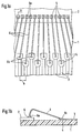
- FIGS. 2a and 2b A rack 1 is shown in FIGS. 2a and 2b which was produced by the method according to the invention.
- the figures are only intended to show the essential content of the invention make it clear and are therefore what the magnitudes and e.g. the length of the bond wires is greatly simplified.
- the printed conductor pattern shown forms as in the case of FIG. 1a known solution shown a grid with each other parallel conductor track ends. The conductor ends 3 but can be much closer to that in comparison to Fig. 1a Component 2 be introduced.
- each component connection 5 is connected via two bonding wires 6 and 7 connected to a conductor track 3.
- the procedure is as follows that the first end designed in the form of a ball 6a of a bonding wire 6 with a connection 5 of the component 2 is shit.
- the pad 4 is not integrated in a conductor track 3, is located spatially separate from the Conductor tracks 3 on the area between the component 2 and the grid of the conductor tracks.
- the end 6b of the bonding wire 6a now the bondhead moved to a conductor track 3, which with this Pad 4 is to be connected.
- the conductor tracks 3 are located in a narrow grid on the subrack at a distance b from each other, which is approximately the distance a corresponds to the component connections. This is possible because in the subrack 1 shown in FIG.
- the width a pad 4 equal to or larger than the sum of the width of the assigned conductor track and the two distances this conductor path to the directly adjacent one Conductors can be without the pads the Traces overlap. But there are also larger distances b conceivable.
- the spherical or ball-shaped end 7a of a second Bond wire 7 is now first welded to the conductor track 3. This is easily possible because of the manufacture this shit connection does not take up as much space on the conductor tracks is claimed as for the preparation of the second Welded joint 7b. The connection can also be very narrow conductor tracks are produced.
- connection surfaces are advantageous 4 in the example shown here in three rows between the component 2 and the grid of the conductor tracks 3 arranged. This way, the available space becomes optimal utilized.
Landscapes
- Wire Bonding (AREA)
- Connections Effected By Soldering, Adhesion, Or Permanent Deformation (AREA)
- Structures For Mounting Electric Components On Printed Circuit Boards (AREA)
Abstract
Description
Claims (5)
- Verfahren zur Herstellung von Bonddrahtverbindungen zwischen den Anschlüssen (5) wenigstens eines auf einem Baugruppenträger (1) angeordneten elektrischen oder elektronischen Bauelements (2) und auf dem Baugruppenträger (1) angeordneten Leiterbahnen (3) durch Ball-Wedge-Bonden, wobei erste Enden der Bonddrähte durch das Bondwerkzeug zunächst kugelartig geformt und anschließend mit den Bauelementanschlüssen verschweißt werden und wobei zweite Enden der Bonddrähte mit dem Bondwerkzeug auf den Leiterbahnen zugeordneten Anschlußflächen breitgequetscht und festgeschweißt werden, dadurch gekennzeichnet, daß die den Leiterbahnen (3) zugeordneten Anschlußflächen (4) zwischen dem Bauelement (2) und den Leiterbahnen (3) und räumlich getrennt von den Leiterbahnen (3) angeordnet sind und daß die Anschlußflächen (4) mit wenigstens einem Teil der Bauelementanschlüsse (5) über erste Bonddrähte (6) und mit den Leiterbahnen (3) über zweite Bonddrähte (7) verbunden werden, wobei jeweils das erste Ende (6a) des ersten Bonddrahtes (6) mit einem Bauelementanschluß (5) und das erste Ende (7a) des zweiten Bonddrahtes (7) mit einer Leiterbahn (3) verbunden wird und das zweite Ende (6b) des ersten Bonddrahtes (6) und das zweiten Ende (7b) des zweiten Bonddrahtes (7) mit der dieser Leiterbahn zugeordneten Anschlußfläche (4) verbunden wird.
- Verfahren nach Anspruch 1, dadurch gekennzeichnet, daß jeder zweite Bauelementanschluß (5) mit einer Anschlußfläche (4) verbunden wird, die mit einer Leiterbahn (3) unmittelbar verbunden ist.
- Baugruppenträger zur Durchführung des Verfahrens nach Anspruch 1, dadurch gekennzeichnet, daß die den Leiterbahnen (3) zugeordneten Anschlußflächen (4) zwischen dem Bauelement (2) und den Enden der Leiterbahnen (3) und räumlich getrennt von den Enden der Leiterbahnen (3) angeordnet sind und daß die Anschlußflächen (4) mit wenigstens einem Teil der Bauelementanschlüsse (5) über erste Bonddrähte (6) und mit den Leiterbahnen (3) über zweite Bonddrähte (7) verbindbar sind, wobei die mit den Bauelementanschlüssen (5) verbindbaren Enden (6a) der ersten Bonddrähte (6) und die mit den Leiterbahnen (3) verbindbaren Enden (7a) der zweiten Bonddrähte (7) eine in der Breite kleinere Anbindungsfläche aufweisen als die mit den Anschlußflächen (4) verbindbaren zweiten Enden (6b) der ersten Drähte (6) und zweiten Enden (7b) der zweiten Drähte (7).
- Baugruppenträger nach Anspruch 3, dadurch gekennzeichnet, daß die Breite einer Anschlußfläche (4) größer ist als die Summe aus der Breite der zugeordneten Leiterbahn (3) und den beiden Abständen dieser Leiterbahn (3) zu den auf dem Baugruppenträger (1) direkt benachbarten Leiterbahnen.
- Baugruppenträger nach Anspruch 3 oder 4, dadurch gekennzeichnet, daß die Anschlußflächen (4) im Raum zwischen dem wenigstens einem Bauelement (2) und den Enden der Leiterbahnen (3) in mehreren Reihen versetzt zueinander angeordnet sind.
Applications Claiming Priority (2)
| Application Number | Priority Date | Filing Date | Title |
|---|---|---|---|
| DE1997103639 DE19703639A1 (de) | 1997-01-31 | 1997-01-31 | Verfahren zur Herstellung von Bonddrahtverbindungen |
| DE19703639 | 1997-01-31 |
Publications (3)
| Publication Number | Publication Date |
|---|---|
| EP0867932A2 true EP0867932A2 (de) | 1998-09-30 |
| EP0867932A3 EP0867932A3 (de) | 2000-05-17 |
| EP0867932B1 EP0867932B1 (de) | 2008-10-15 |
Family
ID=7818941
Family Applications (1)
| Application Number | Title | Priority Date | Filing Date |
|---|---|---|---|
| EP19970119991 Expired - Lifetime EP0867932B1 (de) | 1997-01-31 | 1997-11-14 | Verfahren zur Herstellung von Bonddrahtverbindungen |
Country Status (4)
| Country | Link |
|---|---|
| US (1) | US6232561B1 (de) |
| EP (1) | EP0867932B1 (de) |
| JP (1) | JPH10223673A (de) |
| DE (2) | DE19703639A1 (de) |
Families Citing this family (14)
| Publication number | Priority date | Publication date | Assignee | Title |
|---|---|---|---|---|
| US6657225B1 (en) * | 1998-03-25 | 2003-12-02 | Seiko Epson Corporation | Semiconductor component, active matrix substrate for a liquid crystal display, and methods of manufacturing such component and substrate |
| JP2001015541A (ja) * | 1999-06-28 | 2001-01-19 | Sumitomo Electric Ind Ltd | 半導体装置および半導体装置の製造方法 |
| KR20010080450A (ko) * | 1999-09-16 | 2001-08-22 | 롤페스 요하네스 게라투스 알베르투스 | 와이어 본드 밀도 향상을 위한 와이어 본드된 패키지 |
| KR20010064907A (ko) * | 1999-12-20 | 2001-07-11 | 마이클 디. 오브라이언 | 와이어본딩 방법 및 이를 이용한 반도체패키지 |
| US6429515B1 (en) * | 2000-05-05 | 2002-08-06 | Amkor Technology, Inc. | Long wire IC package |
| KR100400032B1 (ko) * | 2001-02-07 | 2003-09-29 | 삼성전자주식회사 | 와이어 본딩을 통해 기판 디자인을 변경하는 반도체 패키지 |
| WO2002078080A1 (en) * | 2001-03-23 | 2002-10-03 | Koninklijke Philips Electronics N.V. | Chip module with bond-wire connections with small loop height |
| US6908843B2 (en) * | 2001-12-28 | 2005-06-21 | Texas Instruments Incorporated | Method and system of wire bonding using interposer pads |
| DE102009029040A1 (de) * | 2009-08-31 | 2011-03-03 | Robert Bosch Gmbh | Vorrichtung und Verfahren zur Herstellung einer Vorrichtung |
| US8138595B2 (en) * | 2010-03-26 | 2012-03-20 | Stats Chippac Ltd. | Integrated circuit packaging system with an intermediate pad and method of manufacture thereof |
| US8203201B2 (en) * | 2010-03-26 | 2012-06-19 | Stats Chippac Ltd. | Integrated circuit packaging system with leads and method of manufacture thereof |
| CN102762040A (zh) * | 2012-07-20 | 2012-10-31 | 杭州华三通信技术有限公司 | 用于在pcb形成金手指的方法及pcb的加工方法 |
| KR20160095731A (ko) * | 2015-02-04 | 2016-08-12 | 에스케이하이닉스 주식회사 | 패키지 온 패키지 타입 적층 패키지 및 그의 제조방법 |
| DE102015207327A1 (de) | 2015-04-22 | 2016-10-27 | Robert Bosch Gmbh | Schaltungsanordnung für eine elektronische Schaltung |
Family Cites Families (11)
| Publication number | Priority date | Publication date | Assignee | Title |
|---|---|---|---|---|
| JPS5546578A (en) * | 1978-09-30 | 1980-04-01 | Toshiba Corp | Method of mounting integrated circuit |
| JPS56100436A (en) * | 1980-01-17 | 1981-08-12 | Toshiba Corp | Manufacture of semiconductor element |
| US4415115A (en) * | 1981-06-08 | 1983-11-15 | Motorola, Inc. | Bonding means and method |
| JPS58210650A (ja) * | 1982-06-01 | 1983-12-07 | Fujitsu Ltd | 半導体装置 |
| JPS60138931A (ja) * | 1983-12-27 | 1985-07-23 | Mitsubishi Electric Corp | 半導体集積回路装置 |
| JPH02201948A (ja) * | 1989-01-30 | 1990-08-10 | Toshiba Corp | 半導体装置パッケージ |
| JPH03167872A (ja) * | 1989-11-28 | 1991-07-19 | Seiko Epson Corp | 半導体装置用リードフレーム |
| JPH04280462A (ja) * | 1991-03-08 | 1992-10-06 | Mitsubishi Electric Corp | リードフレームおよびこのリードフレームを使用した半導体装置 |
| JPH05243306A (ja) * | 1992-02-28 | 1993-09-21 | Nec Corp | 樹脂封止半導体装置 |
| US5365409A (en) * | 1993-02-20 | 1994-11-15 | Vlsi Technology, Inc. | Integrated circuit package design having an intermediate die-attach substrate bonded to a leadframe |
| US5497032A (en) * | 1993-03-17 | 1996-03-05 | Fujitsu Limited | Semiconductor device and lead frame therefore |
-
1997
- 1997-01-31 DE DE1997103639 patent/DE19703639A1/de not_active Withdrawn
- 1997-11-14 EP EP19970119991 patent/EP0867932B1/de not_active Expired - Lifetime
- 1997-11-14 DE DE59712974T patent/DE59712974D1/de not_active Expired - Lifetime
-
1998
- 1998-01-28 US US09/015,033 patent/US6232561B1/en not_active Expired - Fee Related
- 1998-01-29 JP JP1657998A patent/JPH10223673A/ja active Pending
Also Published As
| Publication number | Publication date |
|---|---|
| JPH10223673A (ja) | 1998-08-21 |
| US6232561B1 (en) | 2001-05-15 |
| EP0867932B1 (de) | 2008-10-15 |
| EP0867932A3 (de) | 2000-05-17 |
| DE19703639A1 (de) | 1998-08-06 |
| DE59712974D1 (de) | 2008-11-27 |
Similar Documents
| Publication | Publication Date | Title |
|---|---|---|
| DE19744266B4 (de) | Drahtbondierungsverfahren | |
| DE69026188T2 (de) | Elektrischer Verbinder | |
| DE69535629T2 (de) | Montage von elektronischen komponenten auf einer leiterplatte | |
| DE69910955T2 (de) | Metallfolie mit Hockerkontakten, Schaltungssubstrat mit der Metallfolie, und Halbleitervorrichtung mit dem Schaltungssubstrat | |
| DE19651122C2 (de) | Halbleiterbauelement mit einem Halbleiterchip und einer Leiterplatte | |
| DE3913221A1 (de) | Halbleiteranordnung | |
| EP0867932B1 (de) | Verfahren zur Herstellung von Bonddrahtverbindungen | |
| DE102005011429A1 (de) | Drahtbondverfahren und Halbleiterbauelement | |
| DE10324598A1 (de) | Halbleitervorrichtung | |
| DE19747105A1 (de) | Bauelement mit gestapelten Halbleiterchips | |
| DE10295972T5 (de) | Nicht in einer Form hergestellte Packung für eine Halbleiteranordnung | |
| DE4207198A1 (de) | Zufuehrungsrahmen und halbleitervorrichtung, welche den zufuehrungsrahmen verwendet | |
| DE69805404T2 (de) | Verfahren zum herstellen kontaktloser karten mit antennenverbindung durch gelötete drähte | |
| DE69737320T2 (de) | Halbleitervorrichtung | |
| DE69628964T2 (de) | Harzvergossenes Halbleiterbauteil und Herstellungsverfahren | |
| DE69004581T2 (de) | Plastikumhüllte Hybrid-Halbleiteranordnung. | |
| DE69723801T2 (de) | Herstellungsverfahren einer Kontaktgitter-Halbleiterpackung | |
| DE69523025T2 (de) | Träger für integrierten Schaltkreis zur Kontaktierung eines anderen Trägers mittels Kontaktkugeln | |
| DE19651549B4 (de) | Anschlußrahmen und Chipgehäuse | |
| DE69118308T2 (de) | Verfahren zur Herstellung einer elektrischen Verbindung für eine integrierte Schaltung | |
| DE69305633T2 (de) | Verfahren und Vorrichtung, um Drähte zwischen einem Halbleiterchip und dem zugehörigen Leiterrahmen anzuschliessen | |
| DE10153666A1 (de) | Kontaktanordnung mit hoher Dichte | |
| DE102020100364B4 (de) | Leistungselektronische Baugruppe mit einem Substrat, einer Hülse und einem Kontaktstift und Verfahren zur Herstellung einer solchen Baugruppe | |
| DE3780630T2 (de) | Verbindung von elektronischen bauteilen untereinander. | |
| DE102013018518A1 (de) | IC-Modul für unterschiedliche Verbindungstechniken |
Legal Events
| Date | Code | Title | Description |
|---|---|---|---|
| PUAI | Public reference made under article 153(3) epc to a published international application that has entered the european phase |
Free format text: ORIGINAL CODE: 0009012 |
|
| AK | Designated contracting states |
Kind code of ref document: A2 Designated state(s): DE FR GB |
|
| AX | Request for extension of the european patent |
Free format text: AL;LT;LV;MK;RO;SI |
|
| PUAL | Search report despatched |
Free format text: ORIGINAL CODE: 0009013 |
|
| AK | Designated contracting states |
Kind code of ref document: A3 Designated state(s): AT BE CH DE DK ES FI FR GB GR IE IT LI LU MC NL PT SE |
|
| AX | Request for extension of the european patent |
Free format text: AL;LT;LV;MK;RO;SI |
|
| 17P | Request for examination filed |
Effective date: 20001117 |
|
| AKX | Designation fees paid |
Free format text: DE FR GB |
|
| R17C | First examination report despatched (corrected) |
Effective date: 20070426 |
|
| GRAP | Despatch of communication of intention to grant a patent |
Free format text: ORIGINAL CODE: EPIDOSNIGR1 |
|
| GRAS | Grant fee paid |
Free format text: ORIGINAL CODE: EPIDOSNIGR3 |
|
| GRAA | (expected) grant |
Free format text: ORIGINAL CODE: 0009210 |
|
| AK | Designated contracting states |
Kind code of ref document: B1 Designated state(s): DE FR GB |
|
| REG | Reference to a national code |
Ref country code: GB Ref legal event code: FG4D Free format text: NOT ENGLISH |
|
| REF | Corresponds to: |
Ref document number: 59712974 Country of ref document: DE Date of ref document: 20081127 Kind code of ref document: P |
|
| PLBE | No opposition filed within time limit |
Free format text: ORIGINAL CODE: 0009261 |
|
| STAA | Information on the status of an ep patent application or granted ep patent |
Free format text: STATUS: NO OPPOSITION FILED WITHIN TIME LIMIT |
|
| 26N | No opposition filed |
Effective date: 20090716 |
|
| PGFP | Annual fee paid to national office [announced via postgrant information from national office to epo] |
Ref country code: GB Payment date: 20091123 Year of fee payment: 13 Ref country code: FR Payment date: 20091202 Year of fee payment: 13 |
|
| PGFP | Annual fee paid to national office [announced via postgrant information from national office to epo] |
Ref country code: DE Payment date: 20110125 Year of fee payment: 14 |
|
| GBPC | Gb: european patent ceased through non-payment of renewal fee |
Effective date: 20101114 |
|
| REG | Reference to a national code |
Ref country code: FR Ref legal event code: ST Effective date: 20110801 |
|
| PG25 | Lapsed in a contracting state [announced via postgrant information from national office to epo] |
Ref country code: FR Free format text: LAPSE BECAUSE OF NON-PAYMENT OF DUE FEES Effective date: 20101130 |
|
| PG25 | Lapsed in a contracting state [announced via postgrant information from national office to epo] |
Ref country code: GB Free format text: LAPSE BECAUSE OF NON-PAYMENT OF DUE FEES Effective date: 20101114 |
|
| REG | Reference to a national code |
Ref country code: DE Ref legal event code: R119 Ref document number: 59712974 Country of ref document: DE Effective date: 20120601 |
|
| PG25 | Lapsed in a contracting state [announced via postgrant information from national office to epo] |
Ref country code: DE Free format text: LAPSE BECAUSE OF NON-PAYMENT OF DUE FEES Effective date: 20120601 |