EP0870616A2 - Verfahren zur Herstellung eines Tintenstrahlkopfes - Google Patents
Verfahren zur Herstellung eines Tintenstrahlkopfes Download PDFInfo
- Publication number
- EP0870616A2 EP0870616A2 EP98302682A EP98302682A EP0870616A2 EP 0870616 A2 EP0870616 A2 EP 0870616A2 EP 98302682 A EP98302682 A EP 98302682A EP 98302682 A EP98302682 A EP 98302682A EP 0870616 A2 EP0870616 A2 EP 0870616A2
- Authority
- EP
- European Patent Office
- Prior art keywords
- actuator board
- plane
- conductive layer
- piezoelectric
- ink jet
- Prior art date
- Legal status (The legal status is an assumption and is not a legal conclusion. Google has not performed a legal analysis and makes no representation as to the accuracy of the status listed.)
- Granted
Links
Images


Classifications
-
- B—PERFORMING OPERATIONS; TRANSPORTING
- B41—PRINTING; LINING MACHINES; TYPEWRITERS; STAMPS
- B41J—TYPEWRITERS; SELECTIVE PRINTING MECHANISMS, i.e. MECHANISMS PRINTING OTHERWISE THAN FROM A FORME; CORRECTION OF TYPOGRAPHICAL ERRORS
- B41J2/00—Typewriters or selective printing mechanisms characterised by the printing or marking process for which they are designed
- B41J2/005—Typewriters or selective printing mechanisms characterised by the printing or marking process for which they are designed characterised by bringing liquid or particles selectively into contact with a printing material
- B41J2/01—Ink jet
- B41J2/135—Nozzles
- B41J2/16—Production of nozzles
- B41J2/1621—Manufacturing processes
- B41J2/164—Manufacturing processes thin film formation
- B41J2/1643—Manufacturing processes thin film formation thin film formation by plating
-
- B—PERFORMING OPERATIONS; TRANSPORTING
- B41—PRINTING; LINING MACHINES; TYPEWRITERS; STAMPS
- B41J—TYPEWRITERS; SELECTIVE PRINTING MECHANISMS, i.e. MECHANISMS PRINTING OTHERWISE THAN FROM A FORME; CORRECTION OF TYPOGRAPHICAL ERRORS
- B41J2/00—Typewriters or selective printing mechanisms characterised by the printing or marking process for which they are designed
- B41J2/005—Typewriters or selective printing mechanisms characterised by the printing or marking process for which they are designed characterised by bringing liquid or particles selectively into contact with a printing material
- B41J2/01—Ink jet
- B41J2/135—Nozzles
- B41J2/14—Structure thereof only for on-demand ink jet heads
- B41J2/14201—Structure of print heads with piezoelectric elements
- B41J2/14209—Structure of print heads with piezoelectric elements of finger type, chamber walls consisting integrally of piezoelectric material
-
- B—PERFORMING OPERATIONS; TRANSPORTING
- B41—PRINTING; LINING MACHINES; TYPEWRITERS; STAMPS
- B41J—TYPEWRITERS; SELECTIVE PRINTING MECHANISMS, i.e. MECHANISMS PRINTING OTHERWISE THAN FROM A FORME; CORRECTION OF TYPOGRAPHICAL ERRORS
- B41J2/00—Typewriters or selective printing mechanisms characterised by the printing or marking process for which they are designed
- B41J2/005—Typewriters or selective printing mechanisms characterised by the printing or marking process for which they are designed characterised by bringing liquid or particles selectively into contact with a printing material
- B41J2/01—Ink jet
- B41J2/135—Nozzles
- B41J2/16—Production of nozzles
- B41J2/1607—Production of print heads with piezoelectric elements
- B41J2/1609—Production of print heads with piezoelectric elements of finger type, chamber walls consisting integrally of piezoelectric material
-
- B—PERFORMING OPERATIONS; TRANSPORTING
- B41—PRINTING; LINING MACHINES; TYPEWRITERS; STAMPS
- B41J—TYPEWRITERS; SELECTIVE PRINTING MECHANISMS, i.e. MECHANISMS PRINTING OTHERWISE THAN FROM A FORME; CORRECTION OF TYPOGRAPHICAL ERRORS
- B41J2/00—Typewriters or selective printing mechanisms characterised by the printing or marking process for which they are designed
- B41J2/005—Typewriters or selective printing mechanisms characterised by the printing or marking process for which they are designed characterised by bringing liquid or particles selectively into contact with a printing material
- B41J2/01—Ink jet
- B41J2/135—Nozzles
- B41J2/16—Production of nozzles
- B41J2/1621—Manufacturing processes
- B41J2/1623—Manufacturing processes bonding and adhesion
-
- B—PERFORMING OPERATIONS; TRANSPORTING
- B41—PRINTING; LINING MACHINES; TYPEWRITERS; STAMPS
- B41J—TYPEWRITERS; SELECTIVE PRINTING MECHANISMS, i.e. MECHANISMS PRINTING OTHERWISE THAN FROM A FORME; CORRECTION OF TYPOGRAPHICAL ERRORS
- B41J2/00—Typewriters or selective printing mechanisms characterised by the printing or marking process for which they are designed
- B41J2/005—Typewriters or selective printing mechanisms characterised by the printing or marking process for which they are designed characterised by bringing liquid or particles selectively into contact with a printing material
- B41J2/01—Ink jet
- B41J2/135—Nozzles
- B41J2/16—Production of nozzles
- B41J2/1621—Manufacturing processes
- B41J2/1632—Manufacturing processes machining
-
- B—PERFORMING OPERATIONS; TRANSPORTING
- B41—PRINTING; LINING MACHINES; TYPEWRITERS; STAMPS
- B41J—TYPEWRITERS; SELECTIVE PRINTING MECHANISMS, i.e. MECHANISMS PRINTING OTHERWISE THAN FROM A FORME; CORRECTION OF TYPOGRAPHICAL ERRORS
- B41J2/00—Typewriters or selective printing mechanisms characterised by the printing or marking process for which they are designed
- B41J2/005—Typewriters or selective printing mechanisms characterised by the printing or marking process for which they are designed characterised by bringing liquid or particles selectively into contact with a printing material
- B41J2/01—Ink jet
- B41J2/135—Nozzles
- B41J2/16—Production of nozzles
- B41J2/1621—Manufacturing processes
- B41J2/164—Manufacturing processes thin film formation
- B41J2/1642—Manufacturing processes thin film formation thin film formation by CVD [chemical vapor deposition]
-
- H—ELECTRICITY
- H10—SEMICONDUCTOR DEVICES; ELECTRIC SOLID-STATE DEVICES NOT OTHERWISE PROVIDED FOR
- H10N—ELECTRIC SOLID-STATE DEVICES NOT OTHERWISE PROVIDED FOR
- H10N30/00—Piezoelectric or electrostrictive devices
- H10N30/01—Manufacture or treatment
- H10N30/08—Shaping or machining of piezoelectric or electrostrictive bodies
- H10N30/085—Shaping or machining of piezoelectric or electrostrictive bodies by machining
- H10N30/088—Shaping or machining of piezoelectric or electrostrictive bodies by machining by cutting or dicing
-
- B—PERFORMING OPERATIONS; TRANSPORTING
- B41—PRINTING; LINING MACHINES; TYPEWRITERS; STAMPS
- B41J—TYPEWRITERS; SELECTIVE PRINTING MECHANISMS, i.e. MECHANISMS PRINTING OTHERWISE THAN FROM A FORME; CORRECTION OF TYPOGRAPHICAL ERRORS
- B41J2/00—Typewriters or selective printing mechanisms characterised by the printing or marking process for which they are designed
- B41J2/005—Typewriters or selective printing mechanisms characterised by the printing or marking process for which they are designed characterised by bringing liquid or particles selectively into contact with a printing material
- B41J2/01—Ink jet
- B41J2/135—Nozzles
- B41J2/14—Structure thereof only for on-demand ink jet heads
- B41J2002/14491—Electrical connection
-
- Y—GENERAL TAGGING OF NEW TECHNOLOGICAL DEVELOPMENTS; GENERAL TAGGING OF CROSS-SECTIONAL TECHNOLOGIES SPANNING OVER SEVERAL SECTIONS OF THE IPC; TECHNICAL SUBJECTS COVERED BY FORMER USPC CROSS-REFERENCE ART COLLECTIONS [XRACs] AND DIGESTS
- Y10—TECHNICAL SUBJECTS COVERED BY FORMER USPC
- Y10T—TECHNICAL SUBJECTS COVERED BY FORMER US CLASSIFICATION
- Y10T29/00—Metal working
- Y10T29/49—Method of mechanical manufacture
- Y10T29/49002—Electrical device making
- Y10T29/49117—Conductor or circuit manufacturing
- Y10T29/49124—On flat or curved insulated base, e.g., printed circuit, etc.
- Y10T29/49155—Manufacturing circuit on or in base
- Y10T29/49156—Manufacturing circuit on or in base with selective destruction of conductive paths
-
- Y—GENERAL TAGGING OF NEW TECHNOLOGICAL DEVELOPMENTS; GENERAL TAGGING OF CROSS-SECTIONAL TECHNOLOGIES SPANNING OVER SEVERAL SECTIONS OF THE IPC; TECHNICAL SUBJECTS COVERED BY FORMER USPC CROSS-REFERENCE ART COLLECTIONS [XRACs] AND DIGESTS
- Y10—TECHNICAL SUBJECTS COVERED BY FORMER USPC
- Y10T—TECHNICAL SUBJECTS COVERED BY FORMER US CLASSIFICATION
- Y10T29/00—Metal working
- Y10T29/49—Method of mechanical manufacture
- Y10T29/49401—Fluid pattern dispersing device making, e.g., ink jet
Definitions
- the present invention relates to a method for producing an ink jet head.
- Communication devices such as a facsimile apparatus or information processors such as a personal computer generally have a recording device capable of recording data including characters and figures on a printing sheet to record the data as visual information.
- a recording device capable of recording data including characters and figures on a printing sheet to record the data as visual information.
- various types of printing methods such as an impact type, a thermal type, and an ink-jet type are used.
- an ink jet recording apparatus using an ink jet type recording which is superior in silence and enables printing on a printing sheet made of various materials has received attention.
- the ink jet apparatus is provided with an ink jet head for printing data such as characters and figures by ejecting ink onto a printing sheet.
- the ink jet head is, as shown in Fig. 15, provided with an actuator board 72 which is made of an piezoelectric element.
- an actuator board 72 which is made of an piezoelectric element.
- a plurality of piezoelectric side walls 73 and concave grooves 74 are alternately arranged.
- Each of the piezoelectric side walls 73 is constructed of a piezoelectric layer which is polarized in a height direction of the side wall 73, each surface of the piezoelectric side walls is provided thereon which an electrode 75.
- the electrode 75 is provided on each surface of the piezoelectric side walls 73 so as to be independent of each other.
- the electrodes 75 are connected conductably with conductive patterns 87 which are formed of conductive layers provided on closing portions 74A for closing back ends of the concave grooves 74 respectively.
- conductive patterns 87 which are formed of conductive layers provided on closing portions 74A for closing back ends of the concave grooves 74 respectively.
- a plurality of lead wires 85 are connected by a soldering way and the like.
- Each of the lead wires 85 is also connected to a printed lead wire 86A provided on a print board 86 by, for example, a soldering operation to connect each electrode 75 to a control unit 88 of the recording apparatus.
- a cover plate 80 provided with an ink supply port 79 is adhered on a grooved side of the actuator board 72.
- This cover plate 80 and each of the concave grooves 74 construct an ejection channel 81 in which ink is to be supplied.
- a nozzle plate 82 for closing each ink chamber 81 is adhered to an end of the actuator 72 and the cover plate 80.
- In the nozzle plate 82 are formed a plurality of nozzles 83 individually corresponding to the ejection channels 81. It is noted that the ejection channel 81 is connected with an ink storing tank not shown through the ink supply port 79.
- the ink jet head constructed as above is produced by the following producing method.
- the actuator board 72 is subjected to a grooving process plural times to make grooves each of which opens at one end of the actuator board 72 in a longitudinal direction thereof (the direction A in Fig. 15) and extends close to another end, whereby a plurality of concave grooves 74 and the piezoelectric side walls 73 are formed so as to be arranged alternately in a width direction (the direction B in Fig. 15) of the board 72, both which extend in the longitudinal direction parallel to each other.
- a conductive layer of metallic thin film is formed by a vacuum deposition method on each upper surface and both side surfaces of the piezoelectric side walls 73 and each upper surface of the closing porion 74A. Thereafter, the upper surfaces of the piezoelectric side walls 73 are subjected to a grinding process to remove the conductive layer therefrom, thereby to form the independent electrode 75 on each side surface of the piezoelectric side wall 73.
- the ink jet head 71 produced as above is installed in the recording apparatus and connected to the ink storing tank through the ink supply port 79 of the cover plate 80, thereby filling each of the ejection channels 81 with ink.
- each of the lead wires 85 is welded to each of the lead wires 86A of the printed board 86 by a soldering operation and the like to connect the electrodes 75 to the control unit 88 respectively.
- a predetermined ejection channel 81 is selected according to data including characters or figures, and driving voltage is applied to the electrodes 75 of the adjacent piezoelectric side walls 73 through the corresponding conductive patterns 87 thereby to deform the piezoelectric side walls 73 to reduce the volume of the ejection channel 81.
- the ink jet head 71 then ejects ink through the ejection channels 81 by an ejection energy resulting from the positive pressure in the inside of the ejection channel 81.
- a plurality of lead wires 85 are needed to be welded by a soldering operation at two points, i.e., the conductive pattern 87 and the lead wire 86A of the printed board 86, to connect each electrode 75 provided on each side surface of the piezoelectric side wall 73 with the control unit 88 of the recording apparatus.
- This may cause a complicated operation to connect the electrode 75, and an increase of soldered portions may causes many inconveniences such as connection failure or cross-connection, resulting in a deterioration in the reliability of connection and the reliability of ink ejection.
- the present invention has been made in view of the above circumstances and has an object to overcome the above problems and to provide a method for producing an ink jet head with high reliability, capable of decreasing steps required for connecting each conductive layer (electrode) connected with a piezoelectric wall (an energy generating means) to a control unit, thereby to enhance the reliability of connection to the control unit.
- a method for producing an ink jet head of this invention comprises the steps of forming an actuator board having a parallelepiped shape with a first plane and a second plane, which is made of piezoelectric ceramic material, forming a plurality of piezoelectric walls by making grooves in the first plane of the actuator board in a longitudinal direction thereof, forming conductive layers made of metallic thin film on a part of both side surfaces of the piezoelectric wall, a first end plane of the actuator board, and an entire surface of the second plane of the actuator board so that the conductive layers are connected with each other, forming a plurality of conductive patterns, each of which is conductably connected with the conductive layer formed on the side surfaces of the piezoelectric wall, on the second plane of the actuator board by forming first grooves in the conductive layer formed on the first end plane of the actuator board in a vertical direction in correspondence with each of the piezoelectric walls and forming second grooves
- the conductive pattern formed on the second plane of the actuator board is divided into a plurality of conductive patterns connected with the conductive layer formed on the side planes of the piezoelectric walls and the remaining conductive layer.
- a method for producing an ink jet head comprising steps of forming an actuator board having a parallelepiped shape with a first plane and a second plane, which is made of piezoelectric ceramic material, forming a plurality of piezoelectric walls by forming grooves in the first plane of the actuator board in a longitudinal direction thereof to alternately make first concave grooves extending from a first end plane of the actuator board to a second end plane and second concave grooves which open at the first end plane of the actuator board and close at the second end plane, forming conductive layers made of metallic thin film on side surfaces of the piezoelectric wall opposite to each other in the first concave groove, the second end plane of the actuator board, and an entire surface of the second plane of the actuator board so that the conductive layers are connected with each other, and on side surfaces of the piezoelectric wall opposite to each other in the second concave groove so as to be connected with the conductive layer on the second plane of the actuator board, forming a
- the conductive layer formed on the second plane of the actuator board is divided into a plurality of individual conductive patterns and the common conductive pattern, so that each of the individual conductive patterns is connected with the conductive layers formed on the side planes of the piezoelectric walls constructing two adjacent second concave grooves between which the first concave groove is provided and the common conductive pattern is connected with the conductive layers formed on the other side planes of the piezoelectric walls.
- the number of conductive patterns can be reduced as compared with the construction of providing independent conductive patterns for every conductive layers formed on the piezoelectric walls, as a result thereof, the connecting operation to the control unit can be reduced. Since the present invention can provide independent conductive patterns as above, it can produce the ink jet head with high reliability.
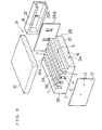
- the ink jet head 1 is provided with an actuator board 2 which is a piezoelectric element in a parallelepiped shape.
- an actuator board 2 which is a piezoelectric element in a parallelepiped shape.
- a plurality of piezoelectric walls 3 (energy generating means) and concave grooves 4 are formed so that the walls 3 and the concave grooves 4 are arranged alternately and parallel to each other.
- Each piezoelectric wall 3 is constructed of a piezoelectric layer which is polarized in a height direction of the wall.
- An electrode 5 is formed on each surface of the piezoelectric walls 3. These electrodes 5 are provided on every side surfaces of the piezoelectric walls 3, independently of each other. As shown in Figs.
- a plurality of divided conductive patterns 7 formed over a back end surface 2B (a first end plane) and a bottom surface 2C (a second plane) of the actuator board 2 are electrically connected with each pair of electrodes 5 and 5 facing to each other inside each concave groove 4.
- Each of the conductive patterns 7 is provided extending in a back and rear direction (the direction A in Fig. 1) of the actuator board 2 on the bottom surface 2C so as to be parallel to each other, and is connected through each of lead wires 6A of a flexible board 6 to the control unit 8 of the recording apparatus for supplying driving voltage, as shown in Fig. 2.
- a cover plate 10 provided with an ink supply port 9 is adhered to a grooved side of the actuator board 2.
- This cover plate 10 and the concave grooves 4 form a plurality of ejection channels 11 in which ink is to be supplied.
- a nozzle plate 12 for closing the ejection channels 11 is adhered to one end of the actuator board 2 and the cover plate 10, in which a plurality of nozzles 13 are formed in one-to-one correspondence to the ejection channels 11. It is noted that each ink chamber 11 is connected to an ink storing chamber not shown through the ink supply port 9.
- the ink jet head 1 having the above structure is produced by a producing method described below, which is explained with reference to Figs 1 to 4.
- the quadrilateral actuator board 2 is made of a piezoelectric ceramic material which has been polarized in a thickness direction thereof.
- a grooving process is applied plural times to make grooves opening at an end of the actuator board 2 in the front and rear direction (the direction A in Fig. 1) and extending close to another end to form plural concave grooves 4 and piezoelectric walls 3 (energy generating means) which extend in the front and rear direction, parallel to each other, such that the walls 3 and the concave grooves 4 appear alternately in a width direction (the direction B in Fig. 1).
- a diamond blade having the thickness capable of forming each concave groove 4 is used for a dicing process.
- Each concave groove 4 opens at a front end surface (a second end plane) 2D of the actuator board 2, but does not reach the back end surface 2B and is closed at the back end.
- a conductive layer Ds of a metallic thin film is formed, for example, by a vacuum deposition continuously on the back end surface 2B and the bottom surface 2C opposite to the grooved side of the actuator board 2, upper surfaces 3A and each upper half of side surfaces of the piezoelectric walls 3, and closing portions 4A formed at rear ends of the concave grooves 4.
- a grinding process is applied to the upper surfaces 3A of the piezoelectric walls 3 to remove the conductive layer Ds therefrom, to form each electrode 5 made of the conductive layer Ds so as to be independently divided on each side surface of the piezoelectric walls 3.
- These electrodes 5 are connected to the conductive layer Ds formed on each of the surfaces 2B and 2C of the actuator board 2 except for the upper surface thereof through the conductive layer Ds of the closing portions 4A of the concave grooves 4.
- the forming method for the conductive layer Ds of the actuator board 2 is not limited to the vacuum deposition and it may be formed, for example, in such a manner that the whole surface of the actuator board 2 including the inside surfaces of the concave grooves 4 are coated with the conductive layer Ds of a metallic thin film by a surface process such as metal plating (for instance, nickel plating), and then the conductive layer Ds of the upper surface (the upper surfaces 3A of the piezoelectric walls 3) and front surface 2D of the actuator board 2 where each concave groove 4 opens is removed by a grinding process and the conductive layer Ds of the bottom surfaces of the concave grooves 4 is removed by a dicing process to provide independently divided electrodes 5.
- a surface process such as metal plating (for instance, nickel plating)
- the portion of the actuator board 2 which does not need to be provided thereon with the conductive layer Ds (for example, the front end surface 2D and the upper surface 3A of each piezoelectric wall 3, etc.), it is also possible to form a resist film prior to the formation of the conductive layer Ds of a metallic thin film and, after the formation of the conductive layer Ds by a surface process such as plating and the like, to chemically remove the conductive layer Ds formed on the above portion by a lift-off system.
- the conductive layer Ds on the back end surface 2B and the bottom surface 2C of the actuator board 2 is divided into a plurality of conductive patterns 7.
- the conductive patterns 7 are formed in a manner that, as shown in Figs. 2 and 3, dividing lateral grooves 15A and 15B (first and second grooves) and a dividing longitudinal groove 16 are formed in the back end surface 2B and the bottom surface 2C of the actuator board 2, whereby the conductive layer Ds on the portions corresponding to the grooves is removed to divide the left conductive layer Ds.
- a plurality of dividing lateral grooves 15A are formed on the back end surface 2B so that an end of each groove 15A is connected with the upper surface 3A of the piezoelectric wall 3 and another end extends to the bottom surface 2C of the actuator board 2.
- a plurality of dividing lateral grooves 15B are formed such that an end of each groove 15B is connected with the corresponding groove 15A provided on the back end surface 2B and these grooves 15B extend parallel to the piezoelectric walls 3.
- the dividing longitudinal groove 16 (third groove) is formed intersecting with the plural dividing lateral grooves 15B to divide the piezoelectric layer Ds into a tip end portion and the other portions provided between the dividing lateral grooves 15B. Accordingly, those lateral grooves 15A and 15B and the longitudinal groove 16 divide the conductive layer Ds on the actuator board 2 into the conductive patterns 7 arranged parallel to each other in the width direction on the back end surface 2B and extend in the front and rear direction on the bottom surface 2C. Each of those conductive patterns 7 is also connected with a pair of electrodes 5 provided facing to each other inside each concave groove 4 through the conductive layer Ds provided on the closing portions 4A formed at the rear ends of the concave grooves 4.
- a diamond blade 17 having the thickness capable of forming a desired groove width is used for a process to make the lateral grooves 15A and 15B and the longitudinal groove 16, as shown in Fig. 4(a).
- a dicing process using the diamond blade 17 is applied to the actuator board 2 to form one lateral groove 15A on the back end surface 2B and one lateral groove 15B on the bottom surface 2C. Thereafter, the dicing process is repeated plural times by parallel moving the diamond blade 17 in the width direction of the actuator board 2 to form a plurality of lateral grooves 15A arranged parallel to each other and a plurality of lateral grooves 15B arranged parallel to each other.
- the longitudinal groove 16 intersecting with the lateral grooves 15B is then formed by a dicing process to divide the conductive layer Ds into individual conductive patterns 7.
- a YAG laser beam 19 which is emitted from a YAG (yttrium-aluminum-garnet) laser oscillator and focused by a f . ⁇ lens 18 may be used.
- the YAG laser beam 19 is scanned onto the back end surface 2B and the bottom surface 2C to form one lateral groove 15A and one lateral groove 15B respectively.
- the scan of the YAG laser beam 19 is repeated plural times by parallel moving the beam in the width direction of the actuator board 2 to form a plurality of lateral grooves 15A arranged parallel to each other and a plurality of lateral grooves 15B arranged parallel to each other.
- the longitudinal groove 16 intersecting with the lateral grooves 15B is then formed by the scan of the YAG laser beam 19 to divide the conductive layer Ds into individual conductive patterns 7.
- the actuator board 2 After the formation of the electrodes 5, the piezoelectric walls 3 (energy generating means), and the conductive patterns 7 on the actuator board 2, the actuator board 2 is coated, for example, with gold-plating and then subjected to a CVD process to protect the gold-plating with an oxide film (SiO film) in order to protect the conductive layer Ds (metallic thin film) of the electrodes 5 and the conductive patterns 7.
- the cover plate 10 is adhered to the grooved side of the actuator board 2 to form, in combination with grooves 4, the ejection channels 11.
- a grinding process is then applied to the front end surface 2D of the actuator board 2 and a front end surface of the cover plate 10 to make them smooth. And, a nozzle plate 12 is adhered to the front end surface 2D so that the ejection channels 11 correspond to the nozzles 13 respectively and to cleaning and the like, to complete the producing of the ink jet head 1.
- the ink jet head 1 produced as above is installed in the recording apparatus and is connected with an ink storing tank through the ink supply port 9 of the cover plate 10. Each of the ejection channels 11 is thus filled with ink.
- the conductive patterns 7 are each connected with the control unit 8 of the recording apparatus through the lead wires 6A of the flexible board 6.
- ink jet head 1 when a predetermined ejection channel 11 is selected according to data including characters or figures to be recorded, negative driving voltage (minus voltage) is applied through the conductive pattern 7 to two electrodes 5 facing to each other in the ejection channel 11 among the electrodes 5 on the adjacent two piezoelectric walls 3 and positive driving voltage (plus voltage) is applied to other two electrodes 5 which are respectively opposite to the above electrodes 5 with respect to each piezoelectric wall 3 to deform the adjacent piezoelectric walls 3 so as to reduce the volume of the ejection channel 11, generating ejection energy to eject ink droplets from the ejection channel 11 through the nozzle 13.
- negative driving voltage minus voltage
- positive driving voltage plus voltage
- both the piezoelectric walls 3 can be made to deform in a direction so as to cause an increase in the volume of the ejection channel 11 between the adjacent piezoelectric walls 3.
- the ejection channel 11 is thus supplied with ink through the ink supply port 9.
- the applied voltage to the piezoelectric walls 3 is then released, the walls 3 return to a straight state, thereby applying pressure to the ink in the ejection channel 11 to eject ink droplets through the nozzle 13. It is not always necessary to apply two types of voltages, positive and negative. It may be arranged such that any one of the voltages is grounded.
- the present invention may also be applied to the ink jet head shown in Figs. 6 to 9.
- the same numerals in Figs. 6 to 9 as in Figs. 1 to 4 indicate the same components.
- a grooving process is applied to an actuator board 2 plural times to make grooves extending entirely in the front and rear direction of the actuator board 2 so that concave grooves 4 and a piezoelectric walls 3 appear alternately and parallel to each other.
- a conductive layer Ds of a metallic thin film is formed, for example, by a vacuum deposition on a back end surface 2B and a bottom surface 2C of the actuator board 2, and both side surfaces of the piezoelectric walls 3.
- These electrodes 5 are connected to the conductive layer Ds formed on each of the surfaces 2B and 2C of the actuator board 2.
- a dicing process or scan with a YAG laser beam 19 is applied to the actuator board 2, as well as in Fig. 4(a) or (b), to form a plurality of dividing lateral grooves 15A and 15B and a dividing longitudinal groove 16 as shown in Figs. 7 and 8, forming a plurality of divided conductive patterns 7 connected respectively to a pair of electrodes 5 provided facing to each other in the concave groove 4.
- a gold-plating process and an oxide film forming process is performed in order to protect the conductive layer Ds.
- a cover plate 10' is then adhered to a grooved side of the actuator board 2.
- the cover plate 10' in cooperation with the concave grooves 4 thus forms the ejection channels 11.
- a manifold 22 having an ink supply port 22A connected to a common ink space B is also adhered to the back end surface 2B of the actuator board 2.
- a grinding process is applied to the front end surface 2D and a front surface of the cover plate 10' to make them smooth.
- a nozzle plate 12 is adhered to the front surface 2D of the actuator board 2 and the cover plate 10' so that the ejection channels 11 are in one-to-one correspondence to the nozzles 13, and is subjected to cleaning and the like, thus completing the producing of the ink jet head 21.
- the producing method for an ink jet head 31 shown in Fig. 9, which is another modification of the first embodiment, is as follows.
- electrodes 5, piezoelectric walls 3 (energy generating means), and conductive patterns 7 are formed on an actuator board 2.
- a cover plate 10' is adhered to a grooved side of the actuator board 2 and, in cooperation with concave grooves 4, forms a plurality of chambers.
- a plate 25 is adhered to a back end surface 2B of the actuator board 2 so as to close alternate chambers.
- a manifold 22 is adhered so as to cover the plate 25. Accordingly, dummy channels 26 in which ink is not supplied and the ejection channels 11 in which ink is supplied through an opening 25A of the plate 25 are formed alternately in the actuator board 2 in the width direction thereof.
- the front end surface 2D of the actuator board 2 and a front surface of the cover plate 10' are subjected to a grinding process and, thereafter, a nozzle plate 12 having a plurality of nozzles 13 in one-to-one correspondence with the ejection channels 11 is adhered to the front surfaces and subjected to cleaning, thus completing the producing of the ink jet head 31.
- a part of the conductive layer Ds is divided by the dividing lateral grooves 15 into a plurality of conductive patterns 7 which are arranged parallel on the actuator board 2 in the width direction and connected respectively with a pair of electrodes 5 facing to each other in the concave groove 4.
- the conductive patterns 7 are separated by the dividing longitudinal groove 16 from the other portion of the conductive layer Ds, so that the conductive patterns 7 can be formed independently of each other.
- the electrodes can be connected to the control unit 8, thus achieving a decrease in connecting operation and enhancing the reliability of the connection between the electrodes and the control unit, thus enabling to produce the ink jet head 1 with high reliability.
- the dicing process or the parallel scan of the YAG laser beam is repeated plural times to form a plurality of lateral grooves 15 thereby to divide the conductive layer Ds into the conductive patterns 7.
- the division and formation of the conductive patterns 7 are conducted in simple processes, further ensuring the division thereof.
- an ink jet head 51 is provided an actuator board 52 which is a piezoelectric element.
- an actuator board 52 which is a piezoelectric element.
- plural concave grooves 64 and 54 (first and second concave grooves) of two kinds extending between a front end surface 52D and a back end surface 52B of the actuator board 52 are formed alternately in the width direction (the direction B in Fig. 10) of the actuator board 52, forming piezoelectric walls 53 (energy generating means) between the adjacent concave grooves 54 and 64.
- Each of the concave grooves 54 has an open end at the front end surface 52D of the actuator board 52 and a closed portion 54A at the back end surface 52B side, the closing portion 54A being formed by raising the bottom of the concave groove 54.
- Each of the concave grooves 64 has open ends at the both back and front end surfaces 52B and 52D.
- On the front end surface 52D of the actuator board 52 formed are vertical grooves 59 going through the actuator board 52 in its thickness direction, which are connected with the front ends of the concave grooves 54 respectively.
- the front ends of the concave grooves 54 thus form steps with respect to the front ends of the concave grooves 64.
- Each of the piezoelectric walls 53 is constructed of two piezoelectric layers, as shown in Fig. 13, which are polarized respectively in the height direction of the wall to be opposite in polarity to each other.
- a pair of electrodes 55 are formed on both surfaces of each piezoelectric wall 53.
- Each pair of electrodes 55 include two electrodes 55A and 55B provided independently of each other on both surfaces of each piezoelectric wall 53.
- the electrodes 55A provided on the walls 53 facing the concave groove 54 are electrically connected with the individual conductive patterns 57 each formed on a side surface 59F of the vertical groove 59 and a bottom surface 52C as shown in Fig. 11.
- two electrodes 55A and 55A positioned outside when seen from the concave groove 64 with respect to the adjacent piezoelectric walls 53 are also conductably connected with the same conductive pattern 57 on the bottom surface 52C, which forming a set.
- the electrodes 55B at the concave groove 64 side are electrically connected with a common conductive pattern 58 formed continuously on the back end of the concave groove 64, the back end surface 52B, and the bottom surface 52C, as shown in Fig. 12.
- the plural individual conductive patterns 57 and the common conductive pattern 58 are, as mentioned later, electrically separated from each other by grooves 65 (first groove) and 66 (second groove).
- the individual conductive patterns 57 are provided extending in the front and rear direction (the direction A in Fig. 10) of the actuator board 52 so as to be arranged parallel to each other on the bottom surface 52C.
- Those conductive patterns 57 are connected with a control unit 56B of the recording apparatus for supplying driving voltage, as well as the common conductive pattern 58, through lead wires 56A of a flexible board 56.
- a cover plate 60 is adhered to a grooved side of the actuator board 52.
- This cover plate 60 and the concave grooves 54 form dummy channels in which ink is not supplied, while the cover plate 60 and the concave grooves 64 form ejection channels 62 in which ink is supplied.
- a nozzle plate 67 is adhered to the front end surface 52D of the actuator board 52 and the cover plate 60 to close the ejection channels 62.
- the nozzle plate 65 is provided with a plurality of nozzles 68 in one-to-one correspondence to the ejection channels 62.
- Adhered on the back end surface 52B of the actuator board 52 is a manifold 63 having an ink supply port 63 connected to a common ink chamber B.
- Each of the ejection channels 62 is connected to an ink storing tank not shown through the common ink chamber B and the ink supply port 63A.
- the ink jet head 51 constructed as above is produced in the following producing method, which is explained with reference to Figs.10 to 12.
- the quadrilateral actuator board 52 is formed such that piezoelectric ceramic layers which are polarized in opposite directions to each other are stacked and adhered. Then, a grooving process is applied to the actuator board 52 plural times to make the concave grooves 54 which open at an end of the actuator board 52 in the front and rear direction and extend close to the other end and the ink concave grooves 64 entirely extending in the front and rear direction so that those grooves 54 and 64 are arranged alternately in the width direction of the actuator board 52, thus forming a plurality of piezoelectric walls 53 extending in the front and rear direction between the adjacent concave grooves 54 and 64.
- a vertical groove 59 is formed at a front end of each concave groove 54, providing an inside step to each concave groove 54 with respect to each ink concave groove 64.
- a diamond blade having the thickness capable of forming each of the concave grooves 54 and 64 is used in a dicing process.
- a conductive layer Ds of a metallic thin film is formed, for example, by a vacuum deposition on the back end surface 52B and the bottom surface 52C opposite to the grooved side of the actuator board 52, upper surfaces 53A and each side surface (including the side surfaces of the vertical grooves 59) of the piezoelectric walls 53.
- a grinding process is applied to the upper surfaces 53A of the piezoelectric walls 53 to remove the conductive layer Ds therefrom. This results in the formation of a pair of electrodes 55 formed of metallic thin film including two electrodes 55A and 55B provided on both side surfaces of the piezoelectric wall 53 respectively so as to be independently divided.
- the electrodes 55B facing to each other in the concave grooves 64 are conductably connected with the conductive layer Ds on the back end surface 52B and the bottom surface 52C of the actuator board 52. Also, the electrodes 55A facing to each in the concave grooves 54 are conductably connected with the conductive layer Ds of the side surface 59F provided in the step between the concave grooves 54 and 64, and the bottom surface 52C of the actuator board 52.
- the forming method for the conductive layer Ds of the actuator board 52 is not limited to the vacuum deposition. It may be formed, for example, in a manner that the whole surface of the actuator board 52 including the inside surfaces of the concave grooves 54 and 64 are covered with the conductive layer Ds of a metallic thin film by a surface process such as metal plating (for instance, nickel plating), and then the conductive layer Ds is removed from the upper surfaces 53A of the piezoelectric walls 53, the closing portions 54A of the concave grooves 54, and front surface 52D of the actuator board 52 by a grinding process, and the conductive layer Ds is removed from the bottom surfaces of the concave grooves 54 and the bottom surfaces 59E of the vertical grooves 59 by a dicing process to divide independently the pairs of electrodes 55.
- a surface process such as metal plating (for instance, nickel plating)
- a laser beam also may be used to remove the conductive layer on the above portions.
- the conductive layer Ds on the bottom surface 52C of the actuator board 52 is divided into a plurality of individual conductive patterns 57 and the common conductive pattern 58.
- a plurality of dividing lateral grooves 65 are formed on the bottom surface of the actuator board 52 so that an end of each groove 65 is connected with each bottom surface 59E of the vertical groove 59 and each groove 65 extends parallel to each concave groove 54.
- a dividing longitudinal groove 66 is formed intersecting with the plural dividing lateral grooves 65 to separate the tip end portion of each individual conductive pattern 57 between the lateral grooves 65 from each other and also from the common conductive pattern 58.
- the lateral grooves 65 and the longitudinal groove 66 are formed by the dicing process or the scanning process using a YAG laser beam similarly to the above embodiment shown in Figs. 4(a) and (b).
- the conductive layer Ds provided on the actuator board 52 is divided into the individual conductive patterns 57 which are arranged parallel to each other in the width direction of the actuator board 52 and extended in the back and rear direction and the common conductive pattern 58 which is other portion except for the individual conductive patterns 57.
- Each of the individual conductive patterns 57 is connected with a set of electrodes 55A and 55A each provided in two adjacent concave grooves 54 respectively at the intermediate concave groove 64 side positioning between the two adjacent concave grooves 54, among the electrode pairs on the piezoelectric walls 53, through the conductive layer on the side surface 59F of the vertical groove 59.
- the common conductive pattern 58 is connected with the electrodes 55B provided on the walls 53 opposite in the concave groove 64 through the conductive layer on the back end surface 52B.
- the actuator board 52 After the formation of the pairs of electrodes 55, the piezoelectric walls 53 (energy generating means), the conductive patterns 57 and 58 on the actuator board 52, the actuator board 52 is coated with, for example, gold-plating and is subjected to a CVD process to protect the gold-plating with an oxide film (SiO film) in order to protect the conductive layer Ds (metallic thin film) provided on each pair of electrodes 55, and on the conductive patterns 57 and 58. After the protection of the conductive layer Ds with the gold-plating and the oxide film, the cover plate 60 is adhered to the grooved side of the actuator board 52 as shown in Fig. 10.
- SiO film oxide film
- the cover plate 60 and the concave grooves 54 constitute the dummy channels 61 and the ejection channels 62 so as to appear alternately.
- a grinding process is applied to the front end surface 52D of the actuator board 52 and the front surface of the cover plate 60 to make them smooth.
- the nozzle plate 67 is adhered to the front surfaces so that the nozzles 68 are in one-to-one correspondence to the ejection channels 62.
- the manifold 63 is also adhered on the back end surface 52B of the actuator board 52. After cleaning, the ink jet head 51 is completely produced.
- each of the ejection channels 62 is filled with ink.
- each of the individual conductive patterns 57 and the common conductive pattern 58 are connected respectively to the control unit 56B of the recording apparatus through the lead wires 56A of the flexible board 56 as shown in Fig. 11.
- a predetermined ejection channel 62 is selected according to data including characters or figures to be recorded.
- Negative driving voltage minus voltage
- positive driving voltage plus voltage
- the individual conductive patterns 57 and the common conductive pattern 58 are divided by one longitudinal groove 66 in the above embodiment, but they may be divided, as shown in Fig. 14, by two longitudinal grooves 66 which intersect with the lateral grooves 65. Accordingly, the individual conductive patterns 57 and the common conductive pattern 58 can be surely divided. Also, in the above embodiment, two longitudinal grooves 66 may be used.
- a part of the conductive layer Ds is divided by the dividing lateral grooves 65 into a plurality of conductive patterns 57 individually for one electrode 55A of the pair of electrodes 55, and the other portion of the conductive layer Ds is divided by the dividing longitudinal groove 66 into the individual conductive patterns 57 and the common conductive pattern 58 connected with another electrode 55B of the pair of electrodes 55.
- the individual conductive patterns 57 are independently of each other connected with the electrodes 55A and, independently therefrom, the common conductive pattern 58 is connected with the electrodes 55B. Accordingly, the number of conductive patterns can be reduced as compared with the structure where common conductive patterns are provided independently for every electrodes. As a result, the connecting operation with respect to the control unit 59 can reduced, preventing the connection failure, and also the individual conductive patterns 57 and the common conductive pattern 58 are provided independently of each other, so that the ink jet head 51 with high reliability can be produced.
- the individual conductive patterns 57 and the common conductive pattern 58 are divided and formed on the front and back ends of the actuator board 52 respectively, such that each of the individual conductive patterns 57 is connected with one electrode 55A of a pair of electrodes 55 at one end of the ejection channel 62 in the lengthwise direction and the common conductive pattern 58 is connected with another electrode 55B of the pair of electrodes 55 at another end of the ejection channel 62 in the lengthwise direction. Accordingly, the conductive patterns 57 and 58 are not required to be arranged with a small pitch and can be surely made independent of each other. The ink jet head 51 with high reliability thus can be produced.
- the conductive patterns 57 and 58 can be made independent and connected with the electrodes 55A and 55B of the electrode pair 55, respectively.
- the individual conductive patterns 57 are divided by the dicing process or the parallel scan of the YAG laser beam to form a plurality of lateral grooves 65, so that the division and formation of the conductive patterns 57 are conducted in simple processes, ensuring the division thereof.
- an ink jet head of the present invention after the conductive layer conductable to all of the electrodes is formed on a surface of the actuator board different from another surface thereof on which ejection channels are formed, a part of the conductive layer is divided into a plurality of conductive patterns each end of which is connected with the electrode, and another end of which is divided from another portion of the conductive layer. This makes it possible to ensure independence of each conductive pattern. Accordingly, an ink jet head with the high reliability on connection between the electrodes and the control unit and also the high reliability on ink ejection.
Landscapes
- Engineering & Computer Science (AREA)
- Manufacturing & Machinery (AREA)
- Particle Formation And Scattering Control In Inkjet Printers (AREA)
Applications Claiming Priority (3)
| Application Number | Priority Date | Filing Date | Title |
|---|---|---|---|
| JP9099397 | 1997-04-09 | ||
| JP09099397A JP3697829B2 (ja) | 1997-04-09 | 1997-04-09 | インクジェットヘッドの製造方法 |
| JP90993/97 | 1997-04-09 |
Publications (3)
| Publication Number | Publication Date |
|---|---|
| EP0870616A2 true EP0870616A2 (de) | 1998-10-14 |
| EP0870616A3 EP0870616A3 (de) | 1999-03-31 |
| EP0870616B1 EP0870616B1 (de) | 2002-06-19 |
Family
ID=14014046
Family Applications (1)
| Application Number | Title | Priority Date | Filing Date |
|---|---|---|---|
| EP19980302682 Expired - Lifetime EP0870616B1 (de) | 1997-04-09 | 1998-03-06 | Verfahren zur Herstellung eines Tintenstrahlkopfes |
Country Status (4)
| Country | Link |
|---|---|
| US (1) | US6070310A (de) |
| EP (1) | EP0870616B1 (de) |
| JP (1) | JP3697829B2 (de) |
| DE (1) | DE69806086T2 (de) |
Cited By (4)
| Publication number | Priority date | Publication date | Assignee | Title |
|---|---|---|---|---|
| WO2003059627A1 (en) * | 2002-01-15 | 2003-07-24 | Xaar Technology Limited | Droplet deposition apparatus |
| EP1911592A1 (de) * | 2006-10-13 | 2008-04-16 | Konica Minolta IJ Technologies, Inc. | Herstellungsverfahren für einen Einspritzkopf und Einspritzkopf |
| EP2450192A1 (de) * | 2010-11-09 | 2012-05-09 | SII Printek Inc | Flüssigkeitsstrahlkopf, Flüssigkeitsausstoßvorrichtung und Verfahren zum Antreiben des Flüssigkeitsstrahlkopfs |
| EP3357697A1 (de) * | 2017-02-03 | 2018-08-08 | SII Printek Inc | Flüssigkeitsausstosskopfchip, flüssigkeitsausstosskopf, flüssigkeitsausstossvorrichtung und herstellungsverfahren für einen flüssigkeitsausstosskopfchip |
Families Citing this family (27)
| Publication number | Priority date | Publication date | Assignee | Title |
|---|---|---|---|---|
| US6722035B1 (en) * | 1995-11-02 | 2004-04-20 | Brother Kogyo Kabushiki Kaisha | Method of manufacturing an ink ejecting device wherein electrodes formed within non-ejecting channels are divided and electrodes formed within ejecting channels are continuous |
| JPH1178030A (ja) * | 1997-09-10 | 1999-03-23 | Brother Ind Ltd | インクジェットヘッドの製造方法 |
| US6578953B2 (en) * | 1999-03-29 | 2003-06-17 | Seiko Epson Corporation | Inkjet recording head, piezoelectric vibration element unit used for the recording head, and method of manufacturing the piezoelectric vibration element unit |
| JP2002178509A (ja) * | 2000-12-12 | 2002-06-26 | Olympus Optical Co Ltd | 液滴噴射装置 |
| JP2002210989A (ja) * | 2001-01-23 | 2002-07-31 | Sharp Corp | インクジェットヘッド及びその製造方法 |
| JP2002283560A (ja) * | 2001-03-23 | 2002-10-03 | Toshiba Tec Corp | インクジェットプリンタヘッド |
| JP4353670B2 (ja) * | 2002-01-23 | 2009-10-28 | シャープ株式会社 | インクジェットヘッドの製造方法 |
| JP2003340580A (ja) * | 2002-05-24 | 2003-12-02 | Konica Minolta Holdings Inc | レーザ加工方法 |
| US7052117B2 (en) | 2002-07-03 | 2006-05-30 | Dimatix, Inc. | Printhead having a thin pre-fired piezoelectric layer |
| US7285161B2 (en) * | 2002-07-23 | 2007-10-23 | Brother Kogyo Kabushiki Kaisha | Water base pigment ink for ink-jet recording |
| JP4182157B2 (ja) * | 2002-08-12 | 2008-11-19 | 株式会社村田製作所 | 表面波装置 |
| US7077511B2 (en) * | 2002-08-26 | 2006-07-18 | Ricoh Printing Systems Ltd. | Housing used in inkjet head |
| US7131718B2 (en) * | 2003-06-20 | 2006-11-07 | Ricoh Printing Systems, Ltd. | Inkjet head and ejection device |
| US8491076B2 (en) | 2004-03-15 | 2013-07-23 | Fujifilm Dimatix, Inc. | Fluid droplet ejection devices and methods |
| US7281778B2 (en) | 2004-03-15 | 2007-10-16 | Fujifilm Dimatix, Inc. | High frequency droplet ejection device and method |
| US20060032841A1 (en) * | 2004-08-10 | 2006-02-16 | Tan Kee C | Forming features in printhead components |
| EP1836056B1 (de) | 2004-12-30 | 2018-11-07 | Fujifilm Dimatix, Inc. | Tintenstrahldruck |
| JP2007077266A (ja) * | 2005-09-14 | 2007-03-29 | Brother Ind Ltd | インクジェット記録用水性インク及び保存液の選択方法 |
| US7988247B2 (en) | 2007-01-11 | 2011-08-02 | Fujifilm Dimatix, Inc. | Ejection of drops having variable drop size from an ink jet printer |
| JP5387525B2 (ja) * | 2010-07-06 | 2014-01-15 | コニカミノルタ株式会社 | インクジェットヘッド |
| JP2012245625A (ja) * | 2011-05-25 | 2012-12-13 | Seiko Epson Corp | 液体噴射ヘッド及び液体噴射装置 |
| JP5882053B2 (ja) * | 2011-12-28 | 2016-03-09 | 太陽誘電株式会社 | 弾性波デバイスの製造方法 |
| JP6157129B2 (ja) * | 2013-02-01 | 2017-07-05 | キヤノン株式会社 | 液体吐出装置、液体吐出装置の製造方法、金属配線の製造方法およびカラーフィルターの製造方法 |
| JP6157130B2 (ja) * | 2013-02-01 | 2017-07-05 | キヤノン株式会社 | 液体吐出装置、液体吐出装置の製造方法、金属配線の製造方法およびカラーフィルターの製造方法 |
| JP7077207B2 (ja) * | 2018-11-09 | 2022-05-30 | エスアイアイ・プリンテック株式会社 | ヘッドチップの製造方法および液体噴射ヘッドの製造方法 |
| JP2022052544A (ja) * | 2020-09-23 | 2022-04-04 | ローム株式会社 | サーマルプリントヘッドの製造方法 |
| JP7558794B2 (ja) * | 2020-12-21 | 2024-10-01 | エスアイアイ・プリンテック株式会社 | ヘッドチップ、液体噴射ヘッド及び液体噴射記録装置 |
Family Cites Families (17)
| Publication number | Priority date | Publication date | Assignee | Title |
|---|---|---|---|---|
| US3984598A (en) * | 1974-02-08 | 1976-10-05 | Universal Oil Products Company | Metal-clad laminates |
| DE3370182D1 (en) * | 1983-01-12 | 1987-04-16 | Siemens Ag | Method of manufacturing an apparatus for reading a two-dimensional charge image with an array |
| DE3306098A1 (de) * | 1983-02-22 | 1984-08-23 | Siemens AG, 1000 Berlin und 8000 München | Piezoelektrisch betriebener schreibkopf mit kanalmatrize |
| US4707081A (en) * | 1985-09-27 | 1987-11-17 | Eastman Kodak Company | Linear light valve arrays having transversely driven electro-optic gates and method of making such arrays |
| CN1003524B (zh) * | 1985-10-14 | 1989-03-08 | 株式会社日立制作所 | 无电浸镀金溶液 |
| JPH01188349A (ja) * | 1988-01-25 | 1989-07-27 | Fuji Electric Co Ltd | インクジェット記録ヘッドの製造方法 |
| DE68906001T2 (de) * | 1988-12-07 | 1993-09-09 | Seiko Epson Corp | Auf abruf arbeitender tintenstrahldruckkopf. |
| JP2744535B2 (ja) * | 1991-07-08 | 1998-04-28 | 株式会社テック | インクジェットプリンタヘッドの製造方法 |
| JP3082540B2 (ja) * | 1993-10-27 | 2000-08-28 | ブラザー工業株式会社 | インクジェットヘッドの駆動装置 |
| US5646661A (en) * | 1993-11-11 | 1997-07-08 | Brother Kogyo Kabushiki Kaisha | Ink ejecting device having alternating ejecting channels and non-ejecting channels |
| JP3186379B2 (ja) * | 1993-11-11 | 2001-07-11 | ブラザー工業株式会社 | インク噴射装置 |
| JP3183010B2 (ja) * | 1993-12-24 | 2001-07-03 | ブラザー工業株式会社 | インク噴射装置 |
| JPH07276624A (ja) * | 1994-04-07 | 1995-10-24 | Tec Corp | インクジェットプリンタヘッド |
| DE59509149D1 (de) * | 1994-08-03 | 2001-05-10 | Francotyp Postalia Gmbh | Anordnung für plattenförmige Piezoaktoren und Verfahren zu deren Herstellung |
| US5818481A (en) * | 1995-02-13 | 1998-10-06 | Minolta Co., Ltd. | Ink jet printing head having a piezoelectric driver member |
| JP3183107B2 (ja) * | 1995-07-17 | 2001-07-03 | ブラザー工業株式会社 | インクジェットヘッドの製造方法 |
| JPH09131866A (ja) * | 1995-11-09 | 1997-05-20 | Brother Ind Ltd | インクジェットヘッドの製造方法 |
-
1997
- 1997-04-09 JP JP09099397A patent/JP3697829B2/ja not_active Expired - Fee Related
-
1998
- 1998-03-06 EP EP19980302682 patent/EP0870616B1/de not_active Expired - Lifetime
- 1998-04-06 US US09/055,406 patent/US6070310A/en not_active Expired - Lifetime
- 1998-04-06 DE DE69806086T patent/DE69806086T2/de not_active Expired - Lifetime
Cited By (10)
| Publication number | Priority date | Publication date | Assignee | Title |
|---|---|---|---|---|
| WO2003059627A1 (en) * | 2002-01-15 | 2003-07-24 | Xaar Technology Limited | Droplet deposition apparatus |
| EP1911592A1 (de) * | 2006-10-13 | 2008-04-16 | Konica Minolta IJ Technologies, Inc. | Herstellungsverfahren für einen Einspritzkopf und Einspritzkopf |
| US8118411B2 (en) | 2006-10-13 | 2012-02-21 | Konica Minolta Ij Technologies, Inc. | Inkjet head manufacturing method and inkjet head |
| EP2450192A1 (de) * | 2010-11-09 | 2012-05-09 | SII Printek Inc | Flüssigkeitsstrahlkopf, Flüssigkeitsausstoßvorrichtung und Verfahren zum Antreiben des Flüssigkeitsstrahlkopfs |
| CN102555477A (zh) * | 2010-11-09 | 2012-07-11 | 精工电子打印科技有限公司 | 液体喷射头、液体喷射装置及液体喷射头的驱动方法 |
| US8702190B2 (en) | 2010-11-09 | 2014-04-22 | Sii Printek Inc. | Liquid jet head, liquid jet apparatus, and method of driving a liquid jet head |
| CN102555477B (zh) * | 2010-11-09 | 2016-01-20 | 精工电子打印科技有限公司 | 液体喷射头、液体喷射装置及液体喷射头的驱动方法 |
| EP3357697A1 (de) * | 2017-02-03 | 2018-08-08 | SII Printek Inc | Flüssigkeitsausstosskopfchip, flüssigkeitsausstosskopf, flüssigkeitsausstossvorrichtung und herstellungsverfahren für einen flüssigkeitsausstosskopfchip |
| CN108382071A (zh) * | 2017-02-03 | 2018-08-10 | 精工电子打印科技有限公司 | 液体喷射头芯片、液体喷射头、液体喷射装置 |
| US10471716B2 (en) | 2017-02-03 | 2019-11-12 | Sii Printek Inc. | Liquid ejecting head chip, liquid ejecting head, and liquid ejecting apparatus |
Also Published As
| Publication number | Publication date |
|---|---|
| JPH10278282A (ja) | 1998-10-20 |
| DE69806086D1 (de) | 2002-07-25 |
| EP0870616A3 (de) | 1999-03-31 |
| US6070310A (en) | 2000-06-06 |
| JP3697829B2 (ja) | 2005-09-21 |
| EP0870616B1 (de) | 2002-06-19 |
| DE69806086T2 (de) | 2002-10-02 |
Similar Documents
| Publication | Publication Date | Title |
|---|---|---|
| EP0870616B1 (de) | Verfahren zur Herstellung eines Tintenstrahlkopfes | |
| US10821730B2 (en) | Ink-jet head having passage unit and actuator units attached to the passage unit, and ink-jet printer having the ink-jet head | |
| US5959643A (en) | Modular drop-on-demand printing apparatus method of manufacture thereof, and method of drop-on-demand printing | |
| CN100393516C (zh) | 喷墨打印机的喷墨头 | |
| JP4419754B2 (ja) | インクジェットヘッド | |
| US7270402B2 (en) | Ink jet head and ink jet printer | |
| JP3951933B2 (ja) | インクジェットヘッド及びこれを有するインクジェットプリンタ | |
| US6783214B2 (en) | Inkjet head having a plurality of pressure chambers | |
| EP1504902B1 (de) | Vorrichtung für die Abgabe von Flüssigkeiten | |
| US20010038404A1 (en) | Inkjet recording head, piezoelectric vibration element unit used for the recording head, and method of manufacturing the piezoelectric vibration element unit | |
| EP0658142B1 (de) | Tintenstrahldruckkopf | |
| JP3876861B2 (ja) | インクジェットヘッド | |
| JP4069832B2 (ja) | インクジェットヘッド | |
| EP1512533B1 (de) | Tintenstrahldruckkopf | |
| JPH0994954A (ja) | インクジェット記録装置 | |
| JP2005059339A (ja) | インクジェットヘッド、及び、このインクジェットヘッドを有するインクジェット記録装置 | |
| US5543009A (en) | Method of manufacturing a sidewall actuator array for an ink jet printhead | |
| JP2005212374A (ja) | インクジェットヘッド、及び、その製造方法 | |
| JPH09300609A (ja) | インクジェットヘッド | |
| JP3680519B2 (ja) | インクジェットヘッドの製造方法 | |
| JP4627655B2 (ja) | インクジェットヘッド及びその製造方法 | |
| JP3922188B2 (ja) | インクジェットヘッド及びインクジェットプリンタ | |
| JP4540296B2 (ja) | インクジェットヘッドの製造方法 | |
| US7219981B2 (en) | Ink-jet head and producing method thereof | |
| JPH0929982A (ja) | インクジェット記録装置 |
Legal Events
| Date | Code | Title | Description |
|---|---|---|---|
| PUAI | Public reference made under article 153(3) epc to a published international application that has entered the european phase |
Free format text: ORIGINAL CODE: 0009012 |
|
| AK | Designated contracting states |
Kind code of ref document: A2 Designated state(s): DE GB |
|
| AX | Request for extension of the european patent |
Free format text: AL;LT;LV;MK;RO;SI |
|
| PUAL | Search report despatched |
Free format text: ORIGINAL CODE: 0009013 |
|
| AK | Designated contracting states |
Kind code of ref document: A3 Designated state(s): AT BE CH DE DK ES FI FR GB GR IE IT LI LU MC NL PT SE |
|
| AX | Request for extension of the european patent |
Free format text: AL;LT;LV;MK;RO;SI |
|
| 17P | Request for examination filed |
Effective date: 19990702 |
|
| AKX | Designation fees paid |
Free format text: DE GB |
|
| R17P | Request for examination filed (corrected) |
Effective date: 19990702 |
|
| RIN1 | Information on inventor provided before grant (corrected) |
Inventor name: ISHIKAWA, HIROYUKI Inventor name: ITO, SUSUMU |
|
| 17Q | First examination report despatched |
Effective date: 20000801 |
|
| RTI1 | Title (correction) |
Free format text: A METHOD FOR PRODUCING AN INK JET HEAD |
|
| GRAG | Despatch of communication of intention to grant |
Free format text: ORIGINAL CODE: EPIDOS AGRA |
|
| GRAG | Despatch of communication of intention to grant |
Free format text: ORIGINAL CODE: EPIDOS AGRA |
|
| GRAH | Despatch of communication of intention to grant a patent |
Free format text: ORIGINAL CODE: EPIDOS IGRA |
|
| GRAH | Despatch of communication of intention to grant a patent |
Free format text: ORIGINAL CODE: EPIDOS IGRA |
|
| GRAA | (expected) grant |
Free format text: ORIGINAL CODE: 0009210 |
|
| AK | Designated contracting states |
Kind code of ref document: B1 Designated state(s): DE GB |
|
| REG | Reference to a national code |
Ref country code: GB Ref legal event code: FG4D |
|
| REF | Corresponds to: |
Ref document number: 69806086 Country of ref document: DE Date of ref document: 20020725 |
|
| PLBE | No opposition filed within time limit |
Free format text: ORIGINAL CODE: 0009261 |
|
| STAA | Information on the status of an ep patent application or granted ep patent |
Free format text: STATUS: NO OPPOSITION FILED WITHIN TIME LIMIT |
|
| 26N | No opposition filed |
Effective date: 20030320 |
|
| PGFP | Annual fee paid to national office [announced via postgrant information from national office to epo] |
Ref country code: GB Payment date: 20160329 Year of fee payment: 19 |
|
| PGFP | Annual fee paid to national office [announced via postgrant information from national office to epo] |
Ref country code: DE Payment date: 20160414 Year of fee payment: 19 |
|
| REG | Reference to a national code |
Ref country code: DE Ref legal event code: R119 Ref document number: 69806086 Country of ref document: DE |
|
| GBPC | Gb: european patent ceased through non-payment of renewal fee |
Effective date: 20170406 |
|
| PG25 | Lapsed in a contracting state [announced via postgrant information from national office to epo] |
Ref country code: DE Free format text: LAPSE BECAUSE OF NON-PAYMENT OF DUE FEES Effective date: 20171103 |
|
| PG25 | Lapsed in a contracting state [announced via postgrant information from national office to epo] |
Ref country code: GB Free format text: LAPSE BECAUSE OF NON-PAYMENT OF DUE FEES Effective date: 20170406 |