EP0872895A2 - Vertikaler Feldeffekttransistor mit isolierter Steuerelektrode, Verfahren zu dessen Herstellung und entsprechende integrierte Schaltung - Google Patents
Vertikaler Feldeffekttransistor mit isolierter Steuerelektrode, Verfahren zu dessen Herstellung und entsprechende integrierte Schaltung Download PDFInfo
- Publication number
- EP0872895A2 EP0872895A2 EP98302765A EP98302765A EP0872895A2 EP 0872895 A2 EP0872895 A2 EP 0872895A2 EP 98302765 A EP98302765 A EP 98302765A EP 98302765 A EP98302765 A EP 98302765A EP 0872895 A2 EP0872895 A2 EP 0872895A2
- Authority
- EP
- European Patent Office
- Prior art keywords
- region
- drain
- source
- electrode
- element isolation
- Prior art date
- Legal status (The legal status is an assumption and is not a legal conclusion. Google has not performed a legal analysis and makes no representation as to the accuracy of the status listed.)
- Granted
Links
Images


Classifications
-
- H—ELECTRICITY
- H10—SEMICONDUCTOR DEVICES; ELECTRIC SOLID-STATE DEVICES NOT OTHERWISE PROVIDED FOR
- H10D—INORGANIC ELECTRIC SEMICONDUCTOR DEVICES
- H10D30/00—Field-effect transistors [FET]
- H10D30/60—Insulated-gate field-effect transistors [IGFET]
- H10D30/67—Thin-film transistors [TFT]
- H10D30/6728—Vertical TFTs
-
- H—ELECTRICITY
- H10—SEMICONDUCTOR DEVICES; ELECTRIC SOLID-STATE DEVICES NOT OTHERWISE PROVIDED FOR
- H10D—INORGANIC ELECTRIC SEMICONDUCTOR DEVICES
- H10D30/00—Field-effect transistors [FET]
- H10D30/01—Manufacture or treatment
- H10D30/021—Manufacture or treatment of FETs having insulated gates [IGFET]
- H10D30/025—Manufacture or treatment of FETs having insulated gates [IGFET] of vertical IGFETs
-
- H—ELECTRICITY
- H10—SEMICONDUCTOR DEVICES; ELECTRIC SOLID-STATE DEVICES NOT OTHERWISE PROVIDED FOR
- H10D—INORGANIC ELECTRIC SEMICONDUCTOR DEVICES
- H10D30/00—Field-effect transistors [FET]
- H10D30/60—Insulated-gate field-effect transistors [IGFET]
- H10D30/63—Vertical IGFETs
Definitions
- This invention relates to semiconductor device, and in particular, to a vertical MOS semiconductor device where the source, channel and drain thereof are perpendicularly arranged on an SOI substrate. This invention also relates to a method of manufacturing such a vertical MOS semiconductor device.
- MOS semiconductor device As a semiconductor device for realizing an increased integration and an increased high speed performance, a MOS semiconductor device which is formed on an SOI (Semiconductor On Insulator) has been known.
- SOI semiconductor On Insulator
- FIG. 6 shows a MOS semiconductor device of lateral structure wherein an element substrate (P-type Si) 22 is superimposed via an SiO 2 insulating layer 21 on a supporting substrate 20 of P-type Si.
- a source 23, a channel 24 and a drain 25 are respectively formed in this element substrate 22, and a gate electrode 27 is formed over the channel 24 with a gate insulating layer 26 being interposed therebetween.
- FIG. 7 shows a semiconductor device of vertical structure which is disclosed in Japanese Patent Unexamined Publication H/5-41521 and wherein a supporting substrate 29 is superimposed on an element substrate 29 in which a drain 30, a channel 31 and a source 32 are arranged vertically, i.e. in a direction perpendicular to the element substrate 29.
- a gate electrode 34 is arranged beside these regions 30, 31 and 32 with a gate insulating layer 33 being interposed therebetween.
- the gate electrode 34, the drain 30, the channel 31 and the source 32 are electrically isolated by an insulating layer 35 formed around them.
- reference numeral 36 denotes a source wiring
- 37 denotes a gate wiring
- 38 denotes a drain wiring.
- the SOI structure shown in FIG. 6 is advantageous in the respect of achieving an increased high-speed of performance, since the electric field in the inversion layer is weakened in the direction perpendicular to the surface of substrate, thereby making it possible to enhance the mobility of carriers.
- the source 23, channel 24 and drain 25 are arranged laterally in this MOS structure, it is accompanied with a problem that the integration degree of elements would be limited.
- an object of the present invention is to provide a vertical semiconductor device, which makes it possible to enhance the integration degree, to simplify the manufacturing method thereof, and to obtain a stabilized performance.
- Another object of the present invention is to provide a method of manufacturing such a vertical semiconductor device.
- the present invention provides a semiconductor device, which is characterized in that a drain region, a channel region and a source region are vertically formed in a region of a silicon substrate which is encircled by an element isolation film formed one upon another vertically in the silicon substrate; that a drain (or source) electrode and a gate electrode are lead out from said drain (or source) region to a surface of said silicon substrate; and that said gate electrode is electrically isolated by a gate-insulating film, while said drain (or source) electrode is electrically isolated by an insulating film.
- the semiconductor device is characterized in that the drain electrode, gate electrode and source electrode are arranged such that one of the electrodes is disposed at a center and surrounded dually by the remaining two electrodes.
- the semiconductor device is also possible to form element isolation films each radially extending from the electrode disposed at the center to the outermost electrode so as to form a plurality of transistors each partitioned by said element isolation films.
- the method of manufacturing the aforementioned semiconductor device according to the present invention is characterized in that said method comprises:
- the method is characterized in that the second step comprises the steps of:
- the second step may be performed by a process of ion-implantation to be effected from the top of a region of the silicon substrate which is encircled by said element isolation film, thereby forming said drain region, said channel region and said source region.
- the fourth step may be performed by the steps of;
- the drain region, channel region and source region are vertically disposed on a silicon substrate, the integration degree of elements can be increased, and at the same time, the generation of parasitic bipolar can be prevented, thus making it possible to realize a stabilized performance.
- a semiconductor device which is high in integration density and stable in performance by a simple process comprising the steps of; forming an element isolation film in a silicon substrate thereby to form a region encircled by the element isolation film; performing an ion-implantation of the region encircled by the element isolation film so as to form a drain region, a channel region and a source region or performing an impurity implantation of the region encircled by the element isolation film after a non-doped polysilicon is deposited on the region so as to form a channel region and source region (or drain region); forming a trench vertically penetrating into a drain region, a channel region and a source region; and forming a gate insulating film on an inner surface of the trench.
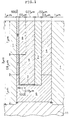
- FIG. 1 shows a cross-sectional view of semiconductor device according to a first embodiment of the present invention.
- a peripheral element isolation film 1 is vertically formed in a silicon substrate 11.
- a drain region 6, a channel region 7 and a source region 8 are successively formed one upon another in the mentioned order in a region encircled by the element isolation film 1.
- a drain electrode 5 and a gate electrode 4 are lead out from the drain region 6 to the surface of the silicon substrate 11.
- An interlayer insulating film 3 is formed between the drain electrode 5 and the gate electrode 4.
- a source insulating film 9 is formed between the gate electrode 4 and the source region 8.
- a gate insulating film 2 is formed between the gate electrode 4 and the drain region 6 as well as between the gate electrode 4 and the channel region 7.
- Lead-out electrodes 401, 501 and 801 are formed on the gate electrode 4, drain electrode 5 and source region 8, respectively (FIG. 2J).
- a protective film 10 is formed covering all over the surface of the device. As a result, a vertical operation transistor having a vertical P-N-P structure is formed between the element isolation films 1.
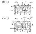
- a square trench 12 is formed in the substrate 11 by means of anisotropic etching such as RIE.
- This trench 12 may be dimensioned such that 1 ⁇ m in width and 3 ⁇ m in depth for instance.
- an oxide film (SiO 2 film) is filled in the trench 12 thereby to form the element isolation film 1.
- a portion of the silicon substrate 11 which is encircled by the element isolation film 1 is etched by means of photolithographic technology, i.e. a plasma etcher to a depth of 1.6 ⁇ m.
- the region thus etched is then subjected to an ion-implantation using a P-type impurity such as boron thereby to form the drain region 6.
- a non-doped polysilicon is deposited all over the surface by means of a low pressure CDV method (LPCVD method), and then the resultant non-doped polysilicon layer is etched back so as to leave a non-doped polysilicon layer 0.6 ⁇ m in thickness only on the surface of the drain region 6.
- an ion-implantation an N-type impurity such as phosphorus is selectively performed, by making use of patterning, on a region of the polysilicon layer excluding a region 5a (at least 0.5 ⁇ m in width) where the drain electrode 5 is to be formed, thereby forming the channel region 7 (600 angstroms).
- a non-doped polysilicon is deposited all over the surface by means of a low pressure CDV method, and then the resultant non-doped polysilicon layer is etched back so as to leave a non-doped polysilicon layer 1 ⁇ m in thickness only on the surface of the channel region 7. Then, an ion-implantation (a P-type impurity such as boron) is selectively performed, by making use of patterning, on a region of the polysilicon layer excluding a region 5b (at least 0.5 ⁇ m in width) where the drain electrode 5 is to be formed, thereby forming the source region 8.
- a P-type impurity such as boron
- a patterned region formed on the source layer 8 and overlapping slightly with the regions 5a and 5b where the drain electrode 5 is to be formed is selectively etched to a depth (1.9 ⁇ m) reaching the drain region 6 by making use of an anisotropic etching such as RIE, thereby forming a trench 14 having a width of 0.47 ⁇ m.
- a gate oxide film 2 (SiO 2 film: 100 angstroms) is formed on the inner wall of the trench 14 which has been formed in the step of FIG. 2F. Then, the space in the trench 14 is buried with polysilicon to be turned into a gate electrode by means of a low pressure CDV method, and the polysilicon thus buried is subjected to an N + doping, thereby forming the gate electrode 4. In simultaneous with this doping of gate electrode, the non-doped polysilicon of the drain regions 5a and 5b is also subjected to an N + doping, thereby forming the drain electrode 5.
- a trench having a depth of 1.9 ⁇ m and a width of 0.2 ⁇ m is formed between the gate electrode 4 and the drain electrode 5, and another trench having a depth of 1 ⁇ m and a width of 0.2 ⁇ m is formed between the gate electrode 4 and the source electrode 8.
- an oxide film (a thermal oxide film or an oxide film by means of CVD) is formed on the inner walls of these trenches, thereby forming the interlayer insulating film 3 and the source insulating film 9.
- an Al-Si is deposited all over the upper surface of the device by means of sputtering and then patterned thereby to form lead-out electrodes 401, 501 and 801 connected with the gate electrode 4, drain electrode 5 and source region 8, respectively.
- a protective layer 10 is deposited all over the upper surface of the device, thus accomplishing a MOS transistor having a vertical P-N-P structure as shown in FIG. 1.
- the drain region 6, the channel 7 and the source region 8 may be formed by making use of only the ion-implantation. In that case, the ion-implantation can be performed directly on the silicon substrate 12 to a desired depth in the step shown in FIG. 2C without performing the etching after the step of photolithography. If the drain region 6, the channel 7 and the source region 8 are formed in this manner, the step of etching as well as the step of depositing polysilicon can be dispensed with, thus making it possible to simplify the manufacturing process.
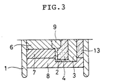
- the aforementioned drain region 6 and source region 8 may be reversed in arrangement as shown in FIG. 3 illustrating a second embodiment of the present invention. Namely, in the structure shown in FIG. 3, the drain region 6 and the source region 8 shown in FIG. 1 are exchanged with each other, so that the drain region 6 is disposed at an upper portion and the source region 8 is disposed at a lower portion, thus forming an N-P-N type transistor.
- the drain electrode 5 of the aforementioned first example is also substituted by a source electrode 13 in this second embodiment.
- FIGS. 4A and 4B show a semiconductor device according to a third embodiment of the present invention.
- the element isolation film 1 is elliptically formed, and each element is formed within this elliptical region encircled by the element isolation film 1.
- an element isolation film la is disposed at the center, around of which the gate electrode 4 is formed.
- the gate electrode 4 is surrounded by source insulating film 9 and then by the source region 8, around of which the drain electrode 5 constituting an outermost region is formed with the interlayer insulating film 3 being interposed therebetween.
- the drain electrode 5 is disposed along the inner wall of the element isolation film 1.
- the thickness of the interlayer insulating film 3 can be made thinner, so that the resultant semiconductor chip can be further miniaturized and at the same time, an electrical interference between the drain and gate can be eliminated, thus making it possible to stabilize the performance of semiconductor device.
- source region 8 and drain region 6 i.e., the drain electrode is substituted by the source electrode
- drain electrode 5 and the gate electrode 4 may be reversed at the center
- the gate electrode 4 and the drain electrode 5 are disposed to surround the source electrode 13. In other words, there is no limitation regarding the arrangement of these electrodes.
- the central element isolation film 1a can be omitted.
- FIG. 5 shows a semiconductor device according to a fourth embodiment of the present invention.
- the semiconductor device according to a fourth embodiment is similar to that shown in FIGS. 4A and 4B except that element isolation films 15, each radially extending from the electrode disposed at the center (the gate electrode 4 in this illustrated embodiment) to the inner wall of the peripheral element isolation film 1, are formed so as to partition the semiconductor device into a plurality of transistors 16 each partitioned by the element isolation films 15.
- this fourth embodiment it is possible to form a plurality of transistors in a single semiconductor device of vertical structure. At the same time, a plurality of transistors can be driven simultaneously with a single central gate electrode 4 (or drain electrode or source electrode).
- the semiconductor devices are exemplified as having an elliptical structure in plan view.
- the present invention is not limited to the elliptical structure, but the shape of the device may be optionally selected, e.g. it may be circular or polygonal.
- the semiconductor device realizes a vertical transistor where a drain region, a channel region and a source region are vertically arranged in high integration degree on a silicon substrate constituting an SOI substrate. Furthermore, since all of the elements can be arranged on a single SOI substrate, the generation of parasitic bipolar can be prevented, thus making it possible to stabilize the performance of the device.
- a trench is formed in a silicon substrate constituting an SOI substrate at first, and then an element isolation film is formed on the inner wall of the trench, after which a drain region, a channel region and a source region are formed in a region encircled by the element isolation film by making use of ion-implantation or by making use of a process comprising the steps of depositing a non-doped polysilicon and implanting an impurity. Therefore, the conventional step of superimposing an element substrate on a supporting substrate can be dispensed with, thus making it possible to obtain a semiconductor device which is high in integration density and stable in performance by a simple process.
Landscapes
- Insulated Gate Type Field-Effect Transistor (AREA)
- Thin Film Transistor (AREA)
- Element Separation (AREA)
Applications Claiming Priority (3)
| Application Number | Priority Date | Filing Date | Title |
|---|---|---|---|
| JP9096163A JPH10290007A (ja) | 1997-04-14 | 1997-04-14 | 半導体装置およびその製造方法 |
| JP9616397 | 1997-04-14 | ||
| JP96163/97 | 1997-04-14 |
Publications (3)
| Publication Number | Publication Date |
|---|---|
| EP0872895A2 true EP0872895A2 (de) | 1998-10-21 |
| EP0872895A3 EP0872895A3 (de) | 1999-02-24 |
| EP0872895B1 EP0872895B1 (de) | 2004-09-29 |
Family
ID=14157680
Family Applications (1)
| Application Number | Title | Priority Date | Filing Date |
|---|---|---|---|
| EP98302765A Expired - Lifetime EP0872895B1 (de) | 1997-04-14 | 1998-04-08 | Vertikaler Feldeffekttransistor mit isolierter Steuerelektrode, Verfahren zu dessen Herstellung und entsprechende integrierte Schaltung |
Country Status (6)
| Country | Link |
|---|---|
| US (1) | US6215150B1 (de) |
| EP (1) | EP0872895B1 (de) |
| JP (1) | JPH10290007A (de) |
| KR (1) | KR100288028B1 (de) |
| DE (1) | DE69826551T2 (de) |
| TW (1) | TW400649B (de) |
Cited By (2)
| Publication number | Priority date | Publication date | Assignee | Title |
|---|---|---|---|---|
| WO2001091192A1 (en) * | 2000-05-25 | 2001-11-29 | Nanogate Ltd. | A thin film field effect transistor |
| WO2004017417A1 (de) | 2002-07-15 | 2004-02-26 | Infineon Technologies Ag | Feldeffekttransistor, zugehörige verwendung und zugehöriges herstellungsverfahren |
Families Citing this family (5)
| Publication number | Priority date | Publication date | Assignee | Title |
|---|---|---|---|---|
| EP0852615B1 (de) * | 1996-07-25 | 2005-12-14 | DuPont Air Products NanoMaterials L.L.C. | Zusammensetzung und verfahren zum chemisch-mechanischen polieren |
| KR100861213B1 (ko) * | 2007-04-17 | 2008-09-30 | 동부일렉트로닉스 주식회사 | 반도체 소자 및 그 제조방법 |
| JP4746600B2 (ja) | 2007-11-01 | 2011-08-10 | シャープ株式会社 | 縦型mosfetの製造方法 |
| WO2015047281A1 (en) * | 2013-09-26 | 2015-04-02 | Intel Corporation | Vertical non-planar semiconductor device for system-on-chip (soc) applications |
| JP7495257B2 (ja) * | 2020-03-24 | 2024-06-04 | 株式会社東海理化電機製作所 | 半導体集積回路、および半導体集積回路の製造方法 |
Family Cites Families (12)
| Publication number | Priority date | Publication date | Assignee | Title |
|---|---|---|---|---|
| JPS60128654A (ja) * | 1983-12-16 | 1985-07-09 | Hitachi Ltd | 半導体集積回路 |
| US4890144A (en) * | 1987-09-14 | 1989-12-26 | Motorola, Inc. | Integrated circuit trench cell |
| US5016067A (en) * | 1988-04-11 | 1991-05-14 | Texas Instruments Incorporated | Vertical MOS transistor |
| JPH01268172A (ja) | 1988-04-20 | 1989-10-25 | Fujitsu Ltd | 半導体装置 |
| JPH03253079A (ja) | 1990-03-02 | 1991-11-12 | Hitachi Ltd | Mos型半導体装置 |
| MY107475A (en) * | 1990-05-31 | 1995-12-30 | Canon Kk | Semiconductor device and method for producing the same. |
| JP2850527B2 (ja) * | 1990-11-20 | 1999-01-27 | 株式会社デンソー | 半導体装置およびその製造方法 |
| US5122848A (en) * | 1991-04-08 | 1992-06-16 | Micron Technology, Inc. | Insulated-gate vertical field-effect transistor with high current drive and minimum overlap capacitance |
| JPH0541521A (ja) | 1991-08-05 | 1993-02-19 | Fujitsu Ltd | 半導体装置及びその製造方法 |
| US5640034A (en) * | 1992-05-18 | 1997-06-17 | Texas Instruments Incorporated | Top-drain trench based resurf DMOS transistor structure |
| US5455190A (en) * | 1994-12-07 | 1995-10-03 | United Microelectronics Corporation | Method of making a vertical channel device using buried source techniques |
| JP3303601B2 (ja) * | 1995-05-19 | 2002-07-22 | 日産自動車株式会社 | 溝型半導体装置 |
-
1997
- 1997-04-14 JP JP9096163A patent/JPH10290007A/ja active Pending
-
1998
- 1998-03-23 TW TW087104285A patent/TW400649B/zh not_active IP Right Cessation
- 1998-03-31 KR KR1019980011124A patent/KR100288028B1/ko not_active Expired - Fee Related
- 1998-04-06 US US09/055,214 patent/US6215150B1/en not_active Expired - Fee Related
- 1998-04-08 EP EP98302765A patent/EP0872895B1/de not_active Expired - Lifetime
- 1998-04-08 DE DE69826551T patent/DE69826551T2/de not_active Expired - Lifetime
Cited By (4)
| Publication number | Priority date | Publication date | Assignee | Title |
|---|---|---|---|---|
| WO2001091192A1 (en) * | 2000-05-25 | 2001-11-29 | Nanogate Ltd. | A thin film field effect transistor |
| US6720617B2 (en) | 2000-05-25 | 2004-04-13 | Nanogate Ltd. | Thin film field effect transistor |
| WO2004017417A1 (de) | 2002-07-15 | 2004-02-26 | Infineon Technologies Ag | Feldeffekttransistor, zugehörige verwendung und zugehöriges herstellungsverfahren |
| US7786530B2 (en) | 2002-07-15 | 2010-08-31 | Infineon Technologies Ag | Vertical field-effect transistor |
Also Published As
| Publication number | Publication date |
|---|---|
| EP0872895A3 (de) | 1999-02-24 |
| DE69826551D1 (de) | 2004-11-04 |
| KR100288028B1 (ko) | 2001-05-02 |
| DE69826551T2 (de) | 2005-10-06 |
| TW400649B (en) | 2000-08-01 |
| JPH10290007A (ja) | 1998-10-27 |
| EP0872895B1 (de) | 2004-09-29 |
| US6215150B1 (en) | 2001-04-10 |
| KR19980080900A (ko) | 1998-11-25 |
Similar Documents
| Publication | Publication Date | Title |
|---|---|---|
| US6406962B1 (en) | Vertical trench-formed dual-gate FET device structure and method for creation | |
| US5939755A (en) | Power IC having high-side and low-side switches in an SOI structure | |
| US5378919A (en) | Semiconductor integrated circuit device with plural gates and plural passive devices | |
| US6204532B1 (en) | Pillar transistor incorporating a body contact | |
| US6313508B1 (en) | Semiconductor device of high-voltage CMOS structure and method of fabricating same | |
| US20080176363A1 (en) | Virtual body-contacted trigate | |
| US6867462B2 (en) | Semiconductor device using an SOI substrate and having a trench isolation and method for fabricating the same | |
| KR100368083B1 (ko) | 수직 채널 전계 효과 트랜지스터 및 그 제조 방법 | |
| KR20000016967A (ko) | 에프이티를포함하는아이씨칩및그형성방법 | |
| JPH09266248A (ja) | 半導体装置 | |
| JP2001060698A (ja) | シリコンオンインシュレータ・ボディコンタクトを形成する方法およびボディコンタクト構造 | |
| JPH09120995A (ja) | 半導体装置およびその製造方法 | |
| JP3888658B2 (ja) | Soi構造を有する半導体素子及びその製造方法 | |
| JP2000040797A (ja) | 半導体素子を有する半導体構造体とその形成方法 | |
| US5929490A (en) | Semiconductor device with an improved body contact hole structure | |
| US5882966A (en) | BiDMOS semiconductor device and method of fabricating the same | |
| US5319235A (en) | Monolithic IC formed of a CCD, CMOS and a bipolar element | |
| JP3716406B2 (ja) | 絶縁ゲート型半導体装置及びその製造方法 | |
| KR100292905B1 (ko) | 절연체상의반도체기판상의바이폴라트랜지스터및그제조방법 | |
| US6114730A (en) | Semiconductor device and its manufacturing method | |
| US6215150B1 (en) | Vertically integrated semiconductor device | |
| US10340362B2 (en) | Spacers for tight gate pitches in field effect transistors | |
| JP2003303960A (ja) | 縦型mos半導体装置およびその製造方法 | |
| KR100319615B1 (ko) | 반도체 장치에서의 소자격리방법 | |
| US7335952B2 (en) | Semiconductor device and manufacturing method therefor |
Legal Events
| Date | Code | Title | Description |
|---|---|---|---|
| PUAI | Public reference made under article 153(3) epc to a published international application that has entered the european phase |
Free format text: ORIGINAL CODE: 0009012 |
|
| AK | Designated contracting states |
Kind code of ref document: A2 Designated state(s): DE FR GB |
|
| AX | Request for extension of the european patent |
Free format text: AL;LT;LV;MK;RO;SI |
|
| PUAL | Search report despatched |
Free format text: ORIGINAL CODE: 0009013 |
|
| AK | Designated contracting states |
Kind code of ref document: A3 Designated state(s): AT BE CH CY DE DK ES FI FR GB GR IE IT LI LU MC NL PT SE |
|
| AX | Request for extension of the european patent |
Free format text: AL;LT;LV;MK;RO;SI |
|
| 17P | Request for examination filed |
Effective date: 19990407 |
|
| AKX | Designation fees paid |
Free format text: DE FR GB |
|
| 17Q | First examination report despatched |
Effective date: 20000209 |
|
| GRAP | Despatch of communication of intention to grant a patent |
Free format text: ORIGINAL CODE: EPIDOSNIGR1 |
|
| GRAS | Grant fee paid |
Free format text: ORIGINAL CODE: EPIDOSNIGR3 |
|
| GRAA | (expected) grant |
Free format text: ORIGINAL CODE: 0009210 |
|
| AK | Designated contracting states |
Kind code of ref document: B1 Designated state(s): DE FR GB |
|
| REG | Reference to a national code |
Ref country code: GB Ref legal event code: FG4D |
|
| REF | Corresponds to: |
Ref document number: 69826551 Country of ref document: DE Date of ref document: 20041104 Kind code of ref document: P |
|
| PLBE | No opposition filed within time limit |
Free format text: ORIGINAL CODE: 0009261 |
|
| STAA | Information on the status of an ep patent application or granted ep patent |
Free format text: STATUS: NO OPPOSITION FILED WITHIN TIME LIMIT |
|
| ET | Fr: translation filed | ||
| 26N | No opposition filed |
Effective date: 20050630 |
|
| PGFP | Annual fee paid to national office [announced via postgrant information from national office to epo] |
Ref country code: DE Payment date: 20110406 Year of fee payment: 14 Ref country code: FR Payment date: 20110426 Year of fee payment: 14 |
|
| PGFP | Annual fee paid to national office [announced via postgrant information from national office to epo] |
Ref country code: GB Payment date: 20110406 Year of fee payment: 14 |
|
| GBPC | Gb: european patent ceased through non-payment of renewal fee |
Effective date: 20120408 |
|
| REG | Reference to a national code |
Ref country code: FR Ref legal event code: ST Effective date: 20121228 |
|
| PG25 | Lapsed in a contracting state [announced via postgrant information from national office to epo] |
Ref country code: GB Free format text: LAPSE BECAUSE OF NON-PAYMENT OF DUE FEES Effective date: 20120408 |
|
| REG | Reference to a national code |
Ref country code: DE Ref legal event code: R119 Ref document number: 69826551 Country of ref document: DE Effective date: 20121101 |
|
| PG25 | Lapsed in a contracting state [announced via postgrant information from national office to epo] |
Ref country code: FR Free format text: LAPSE BECAUSE OF NON-PAYMENT OF DUE FEES Effective date: 20120430 |
|
| PG25 | Lapsed in a contracting state [announced via postgrant information from national office to epo] |
Ref country code: DE Free format text: LAPSE BECAUSE OF NON-PAYMENT OF DUE FEES Effective date: 20121101 |