EP0874460B1 - Digitale Empfängerschaltung mit adaptiver Schwelle für optische Signale - Google Patents
Digitale Empfängerschaltung mit adaptiver Schwelle für optische Signale Download PDFInfo
- Publication number
- EP0874460B1 EP0874460B1 EP98107401A EP98107401A EP0874460B1 EP 0874460 B1 EP0874460 B1 EP 0874460B1 EP 98107401 A EP98107401 A EP 98107401A EP 98107401 A EP98107401 A EP 98107401A EP 0874460 B1 EP0874460 B1 EP 0874460B1
- Authority
- EP
- European Patent Office
- Prior art keywords
- output signal
- adder
- peak detector
- signal
- circuit arrangement
- Prior art date
- Legal status (The legal status is an assumption and is not a legal conclusion. Google has not performed a legal analysis and makes no representation as to the accuracy of the status listed.)
- Expired - Lifetime
Links
- 230000003287 optical effect Effects 0.000 title claims description 51
- 230000003044 adaptive effect Effects 0.000 title description 4
- 230000000295 complement effect Effects 0.000 claims description 20
- 239000003990 capacitor Substances 0.000 description 12
- 238000010586 diagram Methods 0.000 description 7
- 230000008878 coupling Effects 0.000 description 3
- 238000010168 coupling process Methods 0.000 description 3
- 238000005859 coupling reaction Methods 0.000 description 3
- 230000009977 dual effect Effects 0.000 description 3
- 230000005540 biological transmission Effects 0.000 description 1
- 238000006243 chemical reaction Methods 0.000 description 1
- 239000000470 constituent Substances 0.000 description 1
- 230000000694 effects Effects 0.000 description 1
- 230000005669 field effect Effects 0.000 description 1
- 229910044991 metal oxide Inorganic materials 0.000 description 1
- 150000004706 metal oxides Chemical class 0.000 description 1
- 230000035945 sensitivity Effects 0.000 description 1
Images

Classifications
-
- H—ELECTRICITY
- H03—ELECTRONIC CIRCUITRY
- H03K—PULSE TECHNIQUE
- H03K5/00—Manipulating of pulses not covered by one of the other main groups of this subclass
- H03K5/01—Shaping pulses
- H03K5/08—Shaping pulses by limiting; by thresholding; by slicing, i.e. combined limiting and thresholding
- H03K5/082—Shaping pulses by limiting; by thresholding; by slicing, i.e. combined limiting and thresholding with an adaptive threshold
-
- H—ELECTRICITY
- H04—ELECTRIC COMMUNICATION TECHNIQUE
- H04B—TRANSMISSION
- H04B10/00—Transmission systems employing electromagnetic waves other than radio-waves, e.g. infrared, visible or ultraviolet light, or employing corpuscular radiation, e.g. quantum communication
- H04B10/60—Receivers
- H04B10/66—Non-coherent receivers, e.g. using direct detection
- H04B10/69—Electrical arrangements in the receiver
- H04B10/695—Arrangements for optimizing the decision element in the receiver, e.g. by using automatic threshold control
Definitions
- the present invention relates to an adaptive threshold controlled decision circuit suitable for receiving optical digital signals contaminated with ringing components.
- optical interconnection networks are used to transfer optical binary signals between LSI circuits with no format conversion.
- DC-mode optical receivers capable of receiving binary digits of the same value which last for an indefinitely long period of time. Since the required transmission rate is more than several 100 of megabits per second, DC-mode optical receivers with a constant decision threshold and a dynamic range of 10 to 15 dB are not practical because of the difficulty to support a sufficient bandwidth to meet the speed requirement.
- AC-mode optical receivers are also known in the art. This type of optical receivers is used in combination with a coding circuit as an optical data link to take the benefit of its excellent sensitivity characteristic to low optical input levels.
- ringing noise-like components
- the ringing occurs on both high and low level laser outputs when laser diodes are driven at logical-1 (i.e., mark) and logical-0 level (i.e., space), respectively.
- logical-1 i.e., mark
- logical-0 level i.e., space
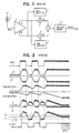
- a prior art optical receiver disclosed in Japanese Laid-Open Patent Specification Hei-8-84160 includes a photodiode 1 for converting optical unipolar input pulses (see Fig. 1) to an electrical current signal which is fed to a differential preamplifier 2.
- the preamplifier produces a pair of voltage signals of opposite logic levels.
- the true output of the preamplifier is supplied to a peak detector 3 and an adder 5, and the complementary output is supplied to a peak detector 4 and an adder 6.
- the difference between the outputs of adders 5 and 6 is determined by a subtractor 7.
- the decision levels of a decision circuit 8, or Schmitt trigger are adaptively controlled by the input signal.
- the difference output of subtractor 7 is higher than threshold V H , the output of decision circuit 8 goes high and when it reduces to a level lower than threshold V L , the output of decision circuit 8 goes low.
- optical receivers are used in both interconnection networks and data links and demand for such applications is enormous, there is therefore a need for dual mode optical receivers.
- a circuit arrangement comprising an amplifier for producing a true output signal and a complementary output signal in response to a digital input signal, a peak detector for receiving the true output signal, a first adder for summing the complementary output signal and an output signal of the peak detector, and a second adder for summing the true output signal and a predetermined constant voltage. Difference between the output signals of the first and second adders is detected. A decision circuit makes a decision on the difference signal to produce a digital output signal.
- a second peak detector having a substantially similar operating characteristic to that of the first peak detector is connected between the source of the constant voltage and the second adder.
- the present invention provides a circuit arrangement comprising an amplifier for producing a true output signal and a complementary output signal in response to a digital input signal, a first peak detector for receiving the true output signal, a second peak detector for receiving the complementary output signal, a first adder for summing the complementary output signal with an output signal of the first peak detector, a second adder for receiving the true output signal and switching circuitry, responsive to a first control signal, for causing a predetermined constant voltage to be summed by the second adder with the true output signal, and responsive to a second control signal, for causing an output signal of the second peak detector to be summed by the second adder. Difference between the output signals of the first and second adders is detected.
- a decision circuit makes a decision on the difference signal to produce a digital output signal.
- each of the first and second peak detectors has a variable time constant value, and wherein the switching circuitry comprises means for setting the time constant values of the first and second peak detectors at a lower value in response to the first control signal, and setting the time constant values of the first and second peak detectors at a higher value in response to the second control signal.
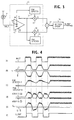
- the optical receiver of this invention comprises a photodiode 11 for converting optical unipolar input pulses to an electrical current signal which is fed to a differential preamplifier 12 of an adaptive threshold controlled decision circuit.
- the preamplifier produces a pair of voltage signals of true and complementary logic levels.
- the true output of the preamplifier is supplied to a peak detector 13 and an adder 15.
- the complementary output of differential preamplifier 12 is supplied only to an adder 16 where it is summed with the output of peak detector 13, and the differential preamplifier 12 has a constant DC voltage supply circuit 19 which feeds a peak detector 14 which is identical in time-constant characteristic to the peak detector 13.
- Adder 15 combines the true output of differential amplifier 12 with the output of peak detector 14. Peak detectors 13 and 14 are of identical circuit configuration.
- Difference between the outputs of adders 15 and 16 is determined by a subtractor 17 and then compared by a decision circuit or Schmitt trigger 18 with a decision threshold V th .
- a decision circuit or Schmitt trigger 18 with a decision threshold V th .
- the voltage produced by the DC voltage supply circuit 19 is a DC voltage of constant level M which is set equal to an average value of the true and complementary output voltages of the differential amplifier 12.
- This constant DC voltage M is coupled via the peak detector 14 to the adder 15 and summed with the amplifier's true output.
- the purpose of the peak detector 14 is to cancel the internal offset voltage of the peak detector 13.
- the input signal shown in part (a) of Fig. 4 is converted by the differential amplifier 12 to a pair of true and complementary varying waveforms as shown in part (b) of Fig. 4.
- Peak detector 13 detects peak voltages of the true output of amplifier 12 and peak detector 14 produces an output voltage corresponding to the constant level M of the voltage supply circuit 19 as shown in part (c) of Fig. 4.
- Adder 15 produces a sum of the true output of amplifier 12 and the constant level output of peak detector 14 and the adder 16 produces a sum of the complementary output of amplifier 12 and the peak level output of peak detector 13 as shown in part (d) of Fig. 4.
- Subtractor 17 produces a voltage representing the difference between the summed output voltages of adders 15 and 16 as shown in part (e) of Fig.
- the output signal of the decision circuit 18 is an accurate representation of the optical input level.
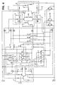
- a portion of the optical receiver is enclosed by a broken-line rectangle 10 and details of this portion are shown in the circuit diagram of Fig. 5.
- Differential preamplifier 12 is of a trans-impedance amplifier configuration in which the true output is fed back to the complementary input and the complementary output is fed back to the true input.
- the preamplifier comprises transistors T1 to T5, resistors R1 to R6 and a capacitor C1.
- Transistor T1 has its emitter coupled via resistor R1 to a voltage terminal V EE and its base coupled via resistor R2 to DC voltage supply circuit 19, the collector of transistor T1 being connected co a circuit node between the emitters of transistors T2 and T3.
- Transistor T2 has is base connected via capacitor C1 co voltage terminal V EE and via resistors R3 and R11 to voltage terminal V EE .
- Transistor T3 has its base connected to input terminal IN and further connected via resistors R4 and R15 to voltage terminal V EE .
- Transistors T4 and T5 have their collectors connected to voltage terminal V CC and their emitters coupled to resistors R3 and R4, respectively.
- the base of transistor T4 is connected to a circuit node between the collector of transistor T2 and resistor R5 and the base of transistor T5 is connected to a circuit node between the collector of transistor T3 and resistor R6, the resistors R5 and R6 being connected to the voltage terminal V CC .
- Peak detector 13 comprises a transistor T7 and a capacitor C2 which is connected across the emitter and collector of transistor T7.
- the base and collector of transistor T7 are connected to the base and collector of transistor T4, respectively.
- the collector of transistor T7 is further connected to voltage terminal V CC .
- the emitter of transistor T7 is further connected to the base of a transistor T10.
- Peak detector 14 comprises a transistor T8 and a capacitor C5 which is connected across the emitter and collector of transistor T8.
- the base of transistor T8 is connected to the DC voltage supply circuit 19 and the collector of transistor T8 is connected to the voltage terminal V CC .
- the emitter of transistor T8 is further connected to the base of a transistor T11.
- DC voltage supply circuit 19 is of a current mirror configuration for setting a current from the preamplifier 12 as a constant current source. Specifically, it comprises resistors R7 to R10 and a transistor T9. Resistors R7, R8 and R9 are connected in series between voltage terminal V CC and the base of transistor T9 and resistor R10 is connected between the emitter of transistor T9 and voltage terminal V CC . A circuit node between resistors R8 and R9 is connected via resistor R2 to the base of transistor T1 of preamplifier 12 and to this circuit node the collector of transistor T9 is also connected.
- Resistors R7 to R10 are determined so that a voltage developed across resistor R7 is substantially equal to an average value of voltages respectively developed across resistors R6 and R7 of the preamplifier 12.
- the voltage developed across resistor R7 is the constant DC voltage M, and this voltage is applied to the base of transistor T8 of peak detector 14.
- Transistors T10 and T11 have their collectors coupled to voltage terminal V CC and their emitters respectively coupled via resistors R12 and R13 to voltage terminal V EE .
- the output of peak detector 13 is amplified by transistor T10 and applied to adder 16.
- Adder 16 is formed with resistors R16, R17 and R18 arranged to combine the amplified peak detector output with a complementary output of amplifier 12 which appears at a circuit node between resistors R4 and R15.
- the output of peak detector 14 is amplified by transistor T11 and applied to adder 15, the adder 15 comprising resistors R19, R20 and R21 arranged to combine the amplified peak detector output with a true output voltage of amplifier 12 which appears at a circuit node between resistors R3 and R11.
- a differential post-amplifier 20 is provided for respectively amplifying the outputs of adders 15 and 16 for application to the subtractor 7.
- This amplifier is formed with transistors T13 to T18 and resistors R22 to R31.
- Transistor T13 has its emitter coupled via resistor R22 to the voltage terminal V EE and its base coupled via resistor R23 to the collector of transistor T18 whose base is coupled via resistor R29 to its collector.
- Transistors T14 and T15 have their emitters coupled together to the collector of transistor T13 and their collectors coupled to the bases of transistors T16 and T17, respectively.
- the base of transistor T14 is connected to the circuit node of resistors R19 to R21 and the base of transistor T15 is connected to the circuit node of resistors R16 to R18.
- Resistors R24 and R25 are connected in series across the collectors of transistors T14 and T15, the circuit node between R24 and R25 being connected via resistor R26 co voltage terminal V CC .
- Transistors T16 and T17 have their collectors connected to voltage terminal V CC and their bases connected to resistors R21 and R17, respectively.
- Transistor T18 has its collector connected via resistor R27 to voltage terminal V CC .
- the emitter of transistor T18 is connected via resistor R28 to voltage terminal V EE to which the emitters of transistors T16 and T17 are also connected via resistors R30 and R31.
- the amplified output of adder 16 is taken from the circuit node between resistors R17 and R31 and the amplified output of adder 15 is taken from the circuit node between resistors R21 and R30.
- a transistor T6 is provided having its base and collector coupled to those of transistor T5 and its emitter coupled to the base of a transistor T12, the collector-emitter path of transistor T12 and a resistor R14 being connected between voltage terminals V CC and V EE .
- the optical receiver of Fig. 5 is modified into a dual mode optical receiver as shown in Fig. 6 by additionally including capacitors C3, C4 and C7 and metal oxide field-effect transistors as switching elements which are classified as K, L and M groups.
- MOSFET switches K1 and K2 are always biased at a constant voltage for coupling capacitor C2 to transistor T17 and the emitter of transistor T10 to the adder 16, regardless of operational modes.
- MOSFET switches L1 and L2 are turned on in response to a DC-mode control signal (e.g., slightly lower than the voltage at terminal V EE ) supplied to a control terminal CTRL for coupling capacitor C5 to transistor T18 to form the peak detector 14 and coupling the emitter of transistor T11 to the adder 15, while switches M1 to M5 are turned off.
- a DC-mode control signal e.g., slightly lower than the voltage at terminal V EE
- MOSFET switches L1 and L2 are turned off and M1 to M6 are turned on in response to an AC-mode control signal (e.g., slightly higher than the voltage at terminal V CC ) supplied to the control terminal CTRL.
- the turn-on of switches M1 to M3 causes capacitors C5, C6 and C7 to be connected in parallel across the emitter and collector of transistor T6 to form a first peak detector.
- the turn-on of switch M4 establishes a connection between the emitter of transistor T12 to the adder 15, so that the output of the first peak detector is applied to the adder 15.
- switches M5 and M6 causes capacitors C3 and C4 to be connected in parallel with capacitor C2 across the emitter and collector of transistor T7 to form a second peak detector identical in characteristic to the first peak detector.
- the output of the second peak detector is supplied through transistor T10 and switch K2 to the adder 16. It is seen that, during the AC mode, the transistor T8 is disconnected from capacitor C5 and the transistor T11 is disconnected from the adder 15. Therefore, the AC-mode optical receiver operates in a characteristic identical to that shown in Fig. 2.
- the peak detectors in DC mode, the peak detectors have low capacitance value and in AC mode their capacitance value is increased.
- the lower capacitance value of the DC mode makes the optical receiver quickly respond to the varying input level, while the higher capacitance value of the AC mode has the effect of reducing the leakage of the peak detectors.
Landscapes
- Physics & Mathematics (AREA)
- Electromagnetism (AREA)
- Engineering & Computer Science (AREA)
- Computer Networks & Wireless Communication (AREA)
- Signal Processing (AREA)
- Nonlinear Science (AREA)
- Optical Communication System (AREA)
- Manipulation Of Pulses (AREA)
- Dc Digital Transmission (AREA)
Claims (10)
- Schaltungsanordnung, aufweisend:einen Verstärker (12) zum Erzeugen eines wahren Ausgangssignals (D) und eines komplementären Ausgangssignals (
D ) ansprechend auf ein digitales Eingangssignal,einen Spitzenwertdetektor (13) zum Empfangen des wahren Ausgangssignals (D),einen ersten Addierer (16) zum Addieren des komplementären Ausgangssignals (D ) und eines Ausgangssignals des Spitzenwertdetektors (13),einen zweiten Addierer (15) zum Addieren des wahren Ausgangssignals (D) und einer vorgegebenen konstanten Spannung,eine Einrichtung (17) zum Erfassen einer Differenz zwischen einem Ausgangssignal (Q ) des ersten Addierers (16) und einem Ausgangssignal (Q) des zweiten Addierers (15) undeine Entscheidungsschaltung (18) zum Fällen einer Entscheidung über die Differenz und zum Erzeugen eines digitalen Ausgangssignals anhand dieser. - Schaltungsanordnung nach Anspruch 1, wobei der Spitzenwertdetektor (13) als ein erster Spitzenwertdetektor arbeitet, weiter aufweisend:eine Gleichspannungsquelle (19) zum Erzeugen der vorgegebenen konstanten Spannung undeinen zweiten Spitzenwertdetektor (14), der zwischen die Gleichspannungsquelle (19) und den zweiten Addierer geschaltet ist, wobei der zweite Spitzenwertdetektor (14) Betriebseigenschaften aufweist, die Betriebseigenschaften des ersten Spitzenwertdetektors (13) im wesentlichen ähneln.
- Schaltungsanordnung nach Anspruch 2, wobei die Gleichspannungsquelle (19) als Teil des Verstärkers (12) ausgebildet ist.
- Schaltungsanordnung, aufweisend:einen Verstärker (12) zum Erzeugen eines wahren Ausgangssignals (D) und eines komplementären Ausgangssignals (D) ansprechend auf ein digitales Eingangssignal,einen ersten Spitzenwertdetektor (13) zum Empfangen des wahren Ausgangssignals (D),einen zweiten Spitzenwertdetektor (14) zum Empfangen des komplementären Ausgangssignals (
D ),einen ersten Addierer (16) zum Addieren des komplementären Ausgangssignals (D ) und eines Ausgangssignals des ersten Spitzenwertdetektors (13),einen zweiten Addierer (15) zum Empfangen des wahren Ausgangssignals (D),eine Schalteinrichtung, die auf ein erstes Steuersignal anspricht, um zu bewirken, daß eine vorgegebene konstante Spannung (M) durch den zweiten Addierer (15) zum wahren Ausgangssignal (D) addiert wird, und die auf ein zweites Steuersignal anspricht, um zu bewirken, daß ein Ausgangssignal des zweiten Spitzenwertdetektors (14) durch den zweiten Addierer (15) summiert wird,eine Einrichtung (17) zum Erfassen einer Differenz zwischen einem Ausgangssignal (Q ) des ersten Addierers (16) und einem Ausgangssignal (Q) des zweiten Addierers (15) undeine Entscheidungsschaltung (18) zum Fällen einer Entscheidung über die Differenz und zum Erzeugen eines digitalen Ausgangssignals anhand dieser. - Schaltungsanordnung nach Anspruch 4, wobei der erste Spitzenwertdetektor (13) und der zweite Spitzenwertdetektor (14) jeweils eine veränderliche Zeitkonstante aufweisen und wobei die Schalteinrichtung eine Einrichtung zum Einstellen der Zeitkonstanten des ersten Spitzenwertdetektors (13) und des zweiten Spitzenwertdetektors (14) auf einen kleineren Wert in Antwort auf das erste Steuersignal und zum Einstellen der Zeitkonstanten des ersten Spitzenwertdetektors (13) und des zweiten Spitzenwertdetektors (14) auf einen größeren Wert in Antwort auf das zweite Steuersignal aufweist.
- Schaltungsanordnung nach Anspruch 4 oder 5, wobei der erste Spitzenwertdetektor (13) und der zweite Spitzenwertdetektor (14) im wesentlichen ähnliche Zeitkonstanten aufweisen.
- Schaltungsanordnung nach Anspruch 4, 5 oder 6, wobei der Verstärker eine Gleichspannungsquelle (19) zum Erzeugen der vorgegebenen konstanten Spannung (M) aufweist.
- Schaltungsanordnung nach einem der Ansprüche 1 bis 7, wobei die vorgegebene konstante Spannung (M) im wesentlichen einem Durchschnittswert des wahren Ausgangssignals (D) und des komplementären Ausgangssignals (
D ) gleicht. - Schaltungsanordnung nach einem der Ansprüche 1 bis 8, weiter aufweisend eine Photodiode (11) zum Umwandeln eines optischen digitalen Eingangssignals in ein entsprechendes elektrisches Signal und zum Zuführen des elektrischen Signals zum Verstärker (12) als das digitale Eingangssignal.
- Optischer Empfänger, aufweisend:eine Photodiode (11) zum Umwandeln eines optischen digitalen Eingangssignals in ein entsprechendes elektrisches Digitalsignal undeine Schaltungsanordnung nach einem der Ansprüche 1 bis 9.
Applications Claiming Priority (3)
| Application Number | Priority Date | Filing Date | Title |
|---|---|---|---|
| JP9105069A JP3039439B2 (ja) | 1997-04-23 | 1997-04-23 | 識別レベル制御回路 |
| JP10506997 | 1997-04-23 | ||
| JP105069/97 | 1997-04-23 |
Publications (3)
| Publication Number | Publication Date |
|---|---|
| EP0874460A2 EP0874460A2 (de) | 1998-10-28 |
| EP0874460A3 EP0874460A3 (de) | 1999-10-20 |
| EP0874460B1 true EP0874460B1 (de) | 2002-03-06 |
Family
ID=14397670
Family Applications (1)
| Application Number | Title | Priority Date | Filing Date |
|---|---|---|---|
| EP98107401A Expired - Lifetime EP0874460B1 (de) | 1997-04-23 | 1998-04-23 | Digitale Empfängerschaltung mit adaptiver Schwelle für optische Signale |
Country Status (4)
| Country | Link |
|---|---|
| US (1) | US6181454B1 (de) |
| EP (1) | EP0874460B1 (de) |
| JP (1) | JP3039439B2 (de) |
| DE (1) | DE69804044T2 (de) |
Families Citing this family (28)
| Publication number | Priority date | Publication date | Assignee | Title |
|---|---|---|---|---|
| JP3327237B2 (ja) | 1998-06-24 | 2002-09-24 | 日本電気株式会社 | アレイ光受信器 |
| JP3514993B2 (ja) * | 1998-12-10 | 2004-04-05 | 日本オプネクスト株式会社 | 光受信回路及び当該回路を用いた光モジュール |
| JP3606143B2 (ja) * | 1999-12-15 | 2005-01-05 | 日本電気株式会社 | オフセット制御回路及びそれを用いた光受信器並びに光通信システム |
| JP2002164855A (ja) * | 2000-11-29 | 2002-06-07 | Oki Electric Ind Co Ltd | 光受信回路 |
| US7173551B2 (en) * | 2000-12-21 | 2007-02-06 | Quellan, Inc. | Increasing data throughput in optical fiber transmission systems |
| US7149256B2 (en) * | 2001-03-29 | 2006-12-12 | Quellan, Inc. | Multilevel pulse position modulation for efficient fiber optic communication |
| US7307569B2 (en) * | 2001-03-29 | 2007-12-11 | Quellan, Inc. | Increasing data throughput in optical fiber transmission systems |
| CA2442922A1 (en) * | 2001-04-04 | 2002-10-17 | Quellan, Inc. | Method and system for decoding multilevel signals |
| US20030030873A1 (en) * | 2001-05-09 | 2003-02-13 | Quellan, Inc. | High-speed adjustable multilevel light modulation |
| AU2003211094A1 (en) * | 2002-02-15 | 2003-09-09 | Quellan, Inc. | Multi-level signal clock recovery technique |
| US6816101B2 (en) * | 2002-03-08 | 2004-11-09 | Quelian, Inc. | High-speed analog-to-digital converter using a unique gray code |
| US7068951B2 (en) * | 2002-04-11 | 2006-06-27 | Optical Communication Products, Inc. | Optical signal receiver with RPM, data and data bar output |
| US20030198478A1 (en) * | 2002-04-23 | 2003-10-23 | Quellan, Inc. | Method and system for generating and decoding a bandwidth efficient multi-level signal |
| EP1357682A1 (de) * | 2002-04-23 | 2003-10-29 | Agilent Technologies, Inc. - a Delaware corporation - | Modulvorrichtung zur optischen Übertragung and hierzu Baugruppe |
| JP2004013681A (ja) * | 2002-06-10 | 2004-01-15 | Bosu & K Consulting Kk | 名刺情報管理システム |
| US7035361B2 (en) * | 2002-07-15 | 2006-04-25 | Quellan, Inc. | Adaptive noise filtering and equalization for optimal high speed multilevel signal decoding |
| US7934144B2 (en) | 2002-11-12 | 2011-04-26 | Quellan, Inc. | High-speed analog-to-digital conversion with improved robustness to timing uncertainty |
| KR101109847B1 (ko) * | 2003-08-07 | 2012-04-06 | ?란 인코포레이티드 | 혼선 제거 방법 및 시스템 |
| US7804760B2 (en) * | 2003-08-07 | 2010-09-28 | Quellan, Inc. | Method and system for signal emulation |
| EP1687929B1 (de) * | 2003-11-17 | 2010-11-10 | Quellan, Inc. | Verfahren und system zur löschung von antennenstörungen |
| US7616700B2 (en) * | 2003-12-22 | 2009-11-10 | Quellan, Inc. | Method and system for slicing a communication signal |
| US7378853B2 (en) * | 2004-02-27 | 2008-05-27 | International Business Machines Corporation | System and method for detecting cable faults for high-speed transmission link |
| US7522883B2 (en) * | 2004-12-14 | 2009-04-21 | Quellan, Inc. | Method and system for reducing signal interference |
| US7725079B2 (en) * | 2004-12-14 | 2010-05-25 | Quellan, Inc. | Method and system for automatic control in an interference cancellation device |
| WO2007127369A2 (en) * | 2006-04-26 | 2007-11-08 | Quellan, Inc. | Method and system for reducing radiated emissions from a communications channel |
| US7855563B2 (en) * | 2007-06-21 | 2010-12-21 | International Business Machines Corporation | Robust cable connectivity test receiver for high-speed data receiver |
| US7873922B2 (en) * | 2007-11-19 | 2011-01-18 | International Business Machines Corporation | Structure for robust cable connectivity test receiver for high-speed data receiver |
| JP5272686B2 (ja) * | 2008-11-28 | 2013-08-28 | 富士通株式会社 | 光受信器、光受信回路および光受信方法 |
Family Cites Families (15)
| Publication number | Priority date | Publication date | Assignee | Title |
|---|---|---|---|---|
| JPS59196636A (ja) | 1983-04-21 | 1984-11-08 | Mitsubishi Electric Corp | 光受信器 |
| JPS62206947A (ja) | 1986-03-06 | 1987-09-11 | Sumitomo Electric Ind Ltd | 光受信機 |
| EP0339727A3 (de) * | 1988-04-27 | 1990-10-31 | Philips Electronics Uk Limited | Schaltung zur Erzeugung eines binären Signals |
| US5025456A (en) | 1989-02-02 | 1991-06-18 | At&T Bell Laboratories | Burst mode digital data receiver |
| US5214319A (en) | 1991-05-28 | 1993-05-25 | Motorola, Inc. | Monotonic pulse detector |
| JP3115739B2 (ja) | 1993-01-27 | 2000-12-11 | シャープ株式会社 | パルス光受信回路 |
| JP3270221B2 (ja) | 1993-10-29 | 2002-04-02 | 株式会社東芝 | 光信号受信回路 |
| JP2656734B2 (ja) | 1994-09-12 | 1997-09-24 | 宮城日本電気株式会社 | 光受信回路 |
| JP2962218B2 (ja) | 1995-02-24 | 1999-10-12 | 日本電気株式会社 | ディジタル光受信回路 |
| JP2655130B2 (ja) | 1995-04-14 | 1997-09-17 | 日本電気株式会社 | ディジタル受信回路 |
| JP3209909B2 (ja) | 1996-01-30 | 2001-09-17 | 富士通株式会社 | バースト光信号受信機 |
| JP2814990B2 (ja) * | 1996-05-20 | 1998-10-27 | 日本電気株式会社 | 光受信回路 |
| JPH1084231A (ja) * | 1996-05-24 | 1998-03-31 | Toshiba Corp | デジタル信号受信回路 |
| JP3576702B2 (ja) | 1996-06-12 | 2004-10-13 | 富士通株式会社 | 可変ハイパスフィルタ |
| JPH10190385A (ja) * | 1996-12-27 | 1998-07-21 | Matsushita Electric Ind Co Ltd | 増幅回路ユニットおよび増幅回路 |
-
1997
- 1997-04-23 JP JP9105069A patent/JP3039439B2/ja not_active Expired - Fee Related
-
1998
- 1998-04-23 US US09/064,505 patent/US6181454B1/en not_active Expired - Lifetime
- 1998-04-23 EP EP98107401A patent/EP0874460B1/de not_active Expired - Lifetime
- 1998-04-23 DE DE69804044T patent/DE69804044T2/de not_active Expired - Lifetime
Also Published As
| Publication number | Publication date |
|---|---|
| US6181454B1 (en) | 2001-01-30 |
| JPH10303992A (ja) | 1998-11-13 |
| EP0874460A3 (de) | 1999-10-20 |
| EP0874460A2 (de) | 1998-10-28 |
| DE69804044T2 (de) | 2002-07-11 |
| JP3039439B2 (ja) | 2000-05-08 |
| DE69804044D1 (de) | 2002-04-11 |
Similar Documents
| Publication | Publication Date | Title |
|---|---|---|
| EP0874460A2 (de) | Digitale Empfängerschaltung mit adaptiver Schwelle für optische Signale | |
| JP3357772B2 (ja) | 受信回路、光受信回路、光受信モジュール及び光配線モジュールセット | |
| US6037841A (en) | Impedance matched CMOS transimpedance amplifier for high-speed fiber optic communications | |
| US5307196A (en) | Optical receiver | |
| US5844445A (en) | Feedback type pre-amplifier | |
| EP0129305B1 (de) | Lichtwellenleiterempfänger | |
| JPH06177664A (ja) | ディジタル光受信回路とトランスインピーダンスアンプ回路とプリアンプ回路 | |
| EP0654896B1 (de) | Transimpedanzverstärkerschaltung mit variablen Rückkopplungs- und Lastwiderstandsschaltungen | |
| CA1215138A (en) | Latching circuits | |
| US4792998A (en) | Receiver for optical digital signals having different amplitudes | |
| JP3394371B2 (ja) | 絶縁伝送装置 | |
| US4257126A (en) | Logarithmic receiver for fiber optic signals | |
| US4336586A (en) | Linear full wave rectifier circuit | |
| JPH08288757A (ja) | ディジタル受信回路 | |
| US4360866A (en) | Linear full wave rectifier and method for providing full wave rectified signals | |
| EP1199799B1 (de) | Signalkompensierungsschaltung und Demodulatorschaltung | |
| JP3214196B2 (ja) | Av光空間伝送の受光回路 | |
| US5561383A (en) | Switchable peak/average detect circuit | |
| JP3181458B2 (ja) | 利得切り替え型光受信増幅回路 | |
| JP3400286B2 (ja) | 受信回路 | |
| JPH08139526A (ja) | 光受信装置 | |
| JPH08279717A (ja) | 光受信器の前置増幅回路 | |
| JP2002290168A (ja) | 光受信器 | |
| JPH0810808B2 (ja) | 単極性符号・双極性符号変換回路 | |
| JPH09246878A (ja) | 電流電圧変換増幅回路 |
Legal Events
| Date | Code | Title | Description |
|---|---|---|---|
| PUAI | Public reference made under article 153(3) epc to a published international application that has entered the european phase |
Free format text: ORIGINAL CODE: 0009012 |
|
| AK | Designated contracting states |
Kind code of ref document: A2 Designated state(s): DE FR GB |
|
| AX | Request for extension of the european patent |
Free format text: AL;LT;LV;MK;RO;SI |
|
| PUAL | Search report despatched |
Free format text: ORIGINAL CODE: 0009013 |
|
| AK | Designated contracting states |
Kind code of ref document: A3 Designated state(s): AT BE CH CY DE DK ES FI FR GB GR IE IT LI LU MC NL PT SE |
|
| AX | Request for extension of the european patent |
Free format text: AL;LT;LV;MK;RO;SI |
|
| RIC1 | Information provided on ipc code assigned before grant |
Free format text: 6H 03K 5/08 A |
|
| 17P | Request for examination filed |
Effective date: 19990910 |
|
| AKX | Designation fees paid |
Free format text: DE FR GB |
|
| GRAG | Despatch of communication of intention to grant |
Free format text: ORIGINAL CODE: EPIDOS AGRA |
|
| 17Q | First examination report despatched |
Effective date: 20010126 |
|
| GRAG | Despatch of communication of intention to grant |
Free format text: ORIGINAL CODE: EPIDOS AGRA |
|
| GRAG | Despatch of communication of intention to grant |
Free format text: ORIGINAL CODE: EPIDOS AGRA |
|
| GRAH | Despatch of communication of intention to grant a patent |
Free format text: ORIGINAL CODE: EPIDOS IGRA |
|
| GRAH | Despatch of communication of intention to grant a patent |
Free format text: ORIGINAL CODE: EPIDOS IGRA |
|
| REG | Reference to a national code |
Ref country code: GB Ref legal event code: IF02 |
|
| GRAA | (expected) grant |
Free format text: ORIGINAL CODE: 0009210 |
|
| AK | Designated contracting states |
Kind code of ref document: B1 Designated state(s): DE FR GB |
|
| REF | Corresponds to: |
Ref document number: 69804044 Country of ref document: DE Date of ref document: 20020411 |
|
| ET | Fr: translation filed | ||
| PLBE | No opposition filed within time limit |
Free format text: ORIGINAL CODE: 0009261 |
|
| STAA | Information on the status of an ep patent application or granted ep patent |
Free format text: STATUS: NO OPPOSITION FILED WITHIN TIME LIMIT |
|
| 26N | No opposition filed |
Effective date: 20021209 |
|
| PGFP | Annual fee paid to national office [announced via postgrant information from national office to epo] |
Ref country code: FR Payment date: 20050408 Year of fee payment: 8 |
|
| PGFP | Annual fee paid to national office [announced via postgrant information from national office to epo] |
Ref country code: GB Payment date: 20050420 Year of fee payment: 8 |
|
| PG25 | Lapsed in a contracting state [announced via postgrant information from national office to epo] |
Ref country code: GB Free format text: LAPSE BECAUSE OF NON-PAYMENT OF DUE FEES Effective date: 20060423 |
|
| GBPC | Gb: european patent ceased through non-payment of renewal fee |
Effective date: 20060423 |
|
| REG | Reference to a national code |
Ref country code: FR Ref legal event code: ST Effective date: 20061230 |
|
| PG25 | Lapsed in a contracting state [announced via postgrant information from national office to epo] |
Ref country code: FR Free format text: LAPSE BECAUSE OF NON-PAYMENT OF DUE FEES Effective date: 20060502 |
|
| PGFP | Annual fee paid to national office [announced via postgrant information from national office to epo] |
Ref country code: DE Payment date: 20170428 Year of fee payment: 20 |
|
| REG | Reference to a national code |
Ref country code: DE Ref legal event code: R071 Ref document number: 69804044 Country of ref document: DE |