EP0875968A2 - Dispositif optique à semiconducteur et méthode de fabrication - Google Patents
Dispositif optique à semiconducteur et méthode de fabrication Download PDFInfo
- Publication number
- EP0875968A2 EP0875968A2 EP98108072A EP98108072A EP0875968A2 EP 0875968 A2 EP0875968 A2 EP 0875968A2 EP 98108072 A EP98108072 A EP 98108072A EP 98108072 A EP98108072 A EP 98108072A EP 0875968 A2 EP0875968 A2 EP 0875968A2
- Authority
- EP
- European Patent Office
- Prior art keywords
- mask
- waveguide
- optical waveguide
- region
- width
- Prior art date
- Legal status (The legal status is an assumption and is not a legal conclusion. Google has not performed a legal analysis and makes no representation as to the accuracy of the status listed.)
- Withdrawn
Links
- 230000003287 optical effect Effects 0.000 title claims abstract description 196
- 239000004065 semiconductor Substances 0.000 title claims abstract description 105
- 238000004519 manufacturing process Methods 0.000 title claims description 19
- 238000006243 chemical reaction Methods 0.000 claims abstract description 43
- 238000000034 method Methods 0.000 claims description 48
- 239000000758 substrate Substances 0.000 claims description 37
- 238000000151 deposition Methods 0.000 claims 1
- 239000010410 layer Substances 0.000 description 157
- VYPSYNLAJGMNEJ-UHFFFAOYSA-N Silicium dioxide Chemical compound O=[Si]=O VYPSYNLAJGMNEJ-UHFFFAOYSA-N 0.000 description 48
- 239000000203 mixture Substances 0.000 description 24
- 239000000377 silicon dioxide Substances 0.000 description 24
- 229910052681 coesite Inorganic materials 0.000 description 23
- 229910052906 cristobalite Inorganic materials 0.000 description 23
- 238000005424 photoluminescence Methods 0.000 description 23
- 229910052682 stishovite Inorganic materials 0.000 description 23
- 229910052905 tridymite Inorganic materials 0.000 description 23
- 238000005530 etching Methods 0.000 description 12
- 238000000206 photolithography Methods 0.000 description 11
- 238000005229 chemical vapour deposition Methods 0.000 description 9
- 239000013307 optical fiber Substances 0.000 description 9
- 229910000530 Gallium indium arsenide Inorganic materials 0.000 description 7
- 230000000903 blocking effect Effects 0.000 description 7
- 238000001312 dry etching Methods 0.000 description 7
- 230000004888 barrier function Effects 0.000 description 4
- 230000010354 integration Effects 0.000 description 4
- 240000002329 Inga feuillei Species 0.000 description 3
- 238000000059 patterning Methods 0.000 description 3
- 230000008878 coupling Effects 0.000 description 2
- 238000010168 coupling process Methods 0.000 description 2
- 238000005859 coupling reaction Methods 0.000 description 2
- 230000006866 deterioration Effects 0.000 description 2
- 238000001451 molecular beam epitaxy Methods 0.000 description 2
- 230000010355 oscillation Effects 0.000 description 2
- 229910000980 Aluminium gallium arsenide Inorganic materials 0.000 description 1
- 229910001218 Gallium arsenide Inorganic materials 0.000 description 1
- 229910052581 Si3N4 Inorganic materials 0.000 description 1
- 230000008033 biological extinction Effects 0.000 description 1
- 230000015572 biosynthetic process Effects 0.000 description 1
- 238000003776 cleavage reaction Methods 0.000 description 1
- 238000004891 communication Methods 0.000 description 1
- 239000012792 core layer Substances 0.000 description 1
- 230000005684 electric field Effects 0.000 description 1
- 125000005842 heteroatom Chemical group 0.000 description 1
- 238000002347 injection Methods 0.000 description 1
- 239000007924 injection Substances 0.000 description 1
- 239000000463 material Substances 0.000 description 1
- 239000002184 metal Substances 0.000 description 1
- 238000002488 metal-organic chemical vapour deposition Methods 0.000 description 1
- 230000007017 scission Effects 0.000 description 1
- 238000000927 vapour-phase epitaxy Methods 0.000 description 1
Images





Classifications
-
- H—ELECTRICITY
- H01—ELECTRIC ELEMENTS
- H01S—DEVICES USING THE PROCESS OF LIGHT AMPLIFICATION BY STIMULATED EMISSION OF RADIATION [LASER] TO AMPLIFY OR GENERATE LIGHT; DEVICES USING STIMULATED EMISSION OF ELECTROMAGNETIC RADIATION IN WAVE RANGES OTHER THAN OPTICAL
- H01S5/00—Semiconductor lasers
- H01S5/10—Construction or shape of the optical resonator, e.g. extended or external cavity, coupled cavities, bent-guide, varying width, thickness or composition of the active region
-
- G—PHYSICS
- G02—OPTICS
- G02B—OPTICAL ELEMENTS, SYSTEMS OR APPARATUS
- G02B6/00—Light guides; Structural details of arrangements comprising light guides and other optical elements, e.g. couplings
- G02B6/10—Light guides; Structural details of arrangements comprising light guides and other optical elements, e.g. couplings of the optical waveguide type
- G02B6/12—Light guides; Structural details of arrangements comprising light guides and other optical elements, e.g. couplings of the optical waveguide type of the integrated circuit kind
- G02B2006/12083—Constructional arrangements
- G02B2006/12121—Laser
-
- G—PHYSICS
- G02—OPTICS
- G02B—OPTICAL ELEMENTS, SYSTEMS OR APPARATUS
- G02B6/00—Light guides; Structural details of arrangements comprising light guides and other optical elements, e.g. couplings
- G02B6/10—Light guides; Structural details of arrangements comprising light guides and other optical elements, e.g. couplings of the optical waveguide type
- G02B6/12—Light guides; Structural details of arrangements comprising light guides and other optical elements, e.g. couplings of the optical waveguide type of the integrated circuit kind
- G02B2006/12166—Manufacturing methods
- G02B2006/12173—Masking
-
- G—PHYSICS
- G02—OPTICS
- G02B—OPTICAL ELEMENTS, SYSTEMS OR APPARATUS
- G02B6/00—Light guides; Structural details of arrangements comprising light guides and other optical elements, e.g. couplings
- G02B6/10—Light guides; Structural details of arrangements comprising light guides and other optical elements, e.g. couplings of the optical waveguide type
- G02B6/12—Light guides; Structural details of arrangements comprising light guides and other optical elements, e.g. couplings of the optical waveguide type of the integrated circuit kind
- G02B2006/12166—Manufacturing methods
- G02B2006/12195—Tapering
-
- H—ELECTRICITY
- H01—ELECTRIC ELEMENTS
- H01S—DEVICES USING THE PROCESS OF LIGHT AMPLIFICATION BY STIMULATED EMISSION OF RADIATION [LASER] TO AMPLIFY OR GENERATE LIGHT; DEVICES USING STIMULATED EMISSION OF ELECTROMAGNETIC RADIATION IN WAVE RANGES OTHER THAN OPTICAL
- H01S5/00—Semiconductor lasers
- H01S5/02—Structural details or components not essential to laser action
- H01S5/026—Monolithically integrated components, e.g. waveguides, monitoring photo-detectors, drivers
- H01S5/0265—Intensity modulators
-
- H—ELECTRICITY
- H01—ELECTRIC ELEMENTS
- H01S—DEVICES USING THE PROCESS OF LIGHT AMPLIFICATION BY STIMULATED EMISSION OF RADIATION [LASER] TO AMPLIFY OR GENERATE LIGHT; DEVICES USING STIMULATED EMISSION OF ELECTROMAGNETIC RADIATION IN WAVE RANGES OTHER THAN OPTICAL
- H01S5/00—Semiconductor lasers
- H01S5/10—Construction or shape of the optical resonator, e.g. extended or external cavity, coupled cavities, bent-guide, varying width, thickness or composition of the active region
- H01S5/1003—Waveguide having a modified shape along the axis, e.g. branched, curved, tapered, voids
- H01S5/1014—Tapered waveguide, e.g. spotsize converter
-
- H—ELECTRICITY
- H01—ELECTRIC ELEMENTS
- H01S—DEVICES USING THE PROCESS OF LIGHT AMPLIFICATION BY STIMULATED EMISSION OF RADIATION [LASER] TO AMPLIFY OR GENERATE LIGHT; DEVICES USING STIMULATED EMISSION OF ELECTROMAGNETIC RADIATION IN WAVE RANGES OTHER THAN OPTICAL
- H01S5/00—Semiconductor lasers
- H01S5/10—Construction or shape of the optical resonator, e.g. extended or external cavity, coupled cavities, bent-guide, varying width, thickness or composition of the active region
- H01S5/1053—Comprising an active region having a varying composition or cross-section in a specific direction
- H01S5/106—Comprising an active region having a varying composition or cross-section in a specific direction varying thickness along the optical axis
-
- H—ELECTRICITY
- H01—ELECTRIC ELEMENTS
- H01S—DEVICES USING THE PROCESS OF LIGHT AMPLIFICATION BY STIMULATED EMISSION OF RADIATION [LASER] TO AMPLIFY OR GENERATE LIGHT; DEVICES USING STIMULATED EMISSION OF ELECTROMAGNETIC RADIATION IN WAVE RANGES OTHER THAN OPTICAL
- H01S5/00—Semiconductor lasers
- H01S5/10—Construction or shape of the optical resonator, e.g. extended or external cavity, coupled cavities, bent-guide, varying width, thickness or composition of the active region
- H01S5/1053—Comprising an active region having a varying composition or cross-section in a specific direction
- H01S5/1064—Comprising an active region having a varying composition or cross-section in a specific direction varying width along the optical axis
-
- H—ELECTRICITY
- H01—ELECTRIC ELEMENTS
- H01S—DEVICES USING THE PROCESS OF LIGHT AMPLIFICATION BY STIMULATED EMISSION OF RADIATION [LASER] TO AMPLIFY OR GENERATE LIGHT; DEVICES USING STIMULATED EMISSION OF ELECTROMAGNETIC RADIATION IN WAVE RANGES OTHER THAN OPTICAL
- H01S5/00—Semiconductor lasers
- H01S5/20—Structure or shape of the semiconductor body to guide the optical wave ; Confining structures perpendicular to the optical axis, e.g. index or gain guiding, stripe geometry, broad area lasers, gain tailoring, transverse or lateral reflectors, special cladding structures, MQW barrier reflection layers
- H01S5/2054—Methods of obtaining the confinement
- H01S5/2077—Methods of obtaining the confinement using lateral bandgap control during growth, e.g. selective growth, mask induced
-
- H—ELECTRICITY
- H01—ELECTRIC ELEMENTS
- H01S—DEVICES USING THE PROCESS OF LIGHT AMPLIFICATION BY STIMULATED EMISSION OF RADIATION [LASER] TO AMPLIFY OR GENERATE LIGHT; DEVICES USING STIMULATED EMISSION OF ELECTROMAGNETIC RADIATION IN WAVE RANGES OTHER THAN OPTICAL
- H01S5/00—Semiconductor lasers
- H01S5/20—Structure or shape of the semiconductor body to guide the optical wave ; Confining structures perpendicular to the optical axis, e.g. index or gain guiding, stripe geometry, broad area lasers, gain tailoring, transverse or lateral reflectors, special cladding structures, MQW barrier reflection layers
- H01S5/22—Structure or shape of the semiconductor body to guide the optical wave ; Confining structures perpendicular to the optical axis, e.g. index or gain guiding, stripe geometry, broad area lasers, gain tailoring, transverse or lateral reflectors, special cladding structures, MQW barrier reflection layers having a ridge or stripe structure
- H01S5/227—Buried mesa structure ; Striped active layer
- H01S5/2272—Buried mesa structure ; Striped active layer grown by a mask induced selective growth
Definitions
- This invention relates to a semiconductor optical device which are applicable for an optical communication, an optical disk device and an optical interconnection and the like and a manufacturing method thereof, and in particular, to the semiconductor optical device which has a spot-size conversion function and a manufacturing method thereof.
- a spot diameter of an optical beam which is emitted from an optical waveguide is small and further, a beam divergence is large. Consequently, it is generally difficult to couple the semiconductor optical device to an optical fiber or a silica-based optical waveguide.
- the semiconductor optical device is conventionally coupled to the optical fiber or the optical waveguide by the use of an optical module with a lens.
- the lens is generally expensive, and further, the position of semiconductor optical device must be adjusted with parts, such as the lens, the optical fiber and the optical waveguide at a high accuracy. This remarkably increases the price of the optical module.
- the semiconductor optical semiconductor device can be coupled to the optical fiber at the high efficiency without the positional adjustment due to the high accuracy by the use of the expensive lens. Consequently, it may be possible to largely reduce the price of the optical module.
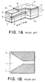
- FP-LD semiconductor optical device of the Fabry-perot laser
- the waveguide of the semiconductor is integrated to convert the optical spot-size.
- the FP-LD has a gain region and a spot-size conversion region on a semiconductor substrate. With such a structure, the spot-size is enlarged by changing the layer thickness of the optical waveguide to realize a narrow beam divergence in the above spot-size conversion region.
- FP-LD FP-LD
- the optical spot-size is enlarged at the laser output facet by the use of a lateral direction taper shape
- the lateral direction taper shape is formed by etching an epitaxial layer which is flatly grow on the entire surface of the substrate without using the selective growth method.
- the spot-size conversion region (namely, an active region) must be formed within the length between 200 ⁇ m and 300 ⁇ m. Consequently, the device yield for each wafer is reduced. Further, the photo-lithography steps must be twice carried out to form the selective growth mask, and the mesa-etching process must be also performed to form the waveguide. As a result, the manufacturing process inevitably becomes complicated.
- the above-mentioned problem may be solved because the lateral taper shape having the optical gain is formed by etching the semiconductor active layer in the second conventional reference.
- the semiconductor layer must be processed in a sub-micron order at the tip portion of the tapered waveguide. Consequently, it is difficult to form the waveguide at the high accuracy by the use of the dry method in addition to the wet method. As a result, it is also difficult to uniformly fabricate the taper shape and to excellently reproduce the device characteristic.
- the device characteristic including the beam divergence largely depends upon the stripe width of the active layer in the first conventional reference. Consequently, it is difficult to stably fabricate the device having the narrow beam divergence on the condition that the excellent characteristic, the reproducibility and the uniformity of the shape are kept.
- the process accuracy is slightly increased in the dry method as compared to the patterning due to the wet method to form the optical waveguide.
- the active layer is damaged from the side surface in this case.
- the optical spot is formed into an approximately circular shape at the output facet with the small emission angle.
- the circular spot shape is realized only by changing the layer thickness like the first conventional reference or by forming the lateral taper shape like the second conventional reference. Consequently, the design flexibility of the device parameters, such as, the active layer structure, the active layer width and the taper shape, is remarkably restricted.
- a semiconductor optical device has a gain region for oscillating a laser light beam and a spot-size conversion region for converting a spot-size of the laser light beam emitted from the gain region. Further, an optical waveguide is formed by the use of a selective growth mask along the gain region and the spot-size conversion region.
- the optical waveguide includes a waveguide taper portion and has a width and a facet.
- the width gradually becomes narrower towards the facet.
- the waveguide taper portion is tapered along a direction from the gain region towards the facet.
- both the mask width and the opening width of the selective growth mask are formed in the taper form.
- the optical waveguide is directly formed only by the use of the selective growth without the etching process. If the optical waveguide is formed by the use of the etching process, the epitaxial growth layer having the layer thickness of between about 0.6 ⁇ m and 1.5 ⁇ m must be etched. It is difficult to process the semiconductor layer having the above layer thickness in the sub-micron order with the high accuracy and the excellent reproducibility.
- the accuracy, the reproducibility and the uniformity of the optical waveguide depends upon the accuracy, the reproducibility and the uniformity of the selective growth mask.
- the semiconductor layer can be processed in the sub-micron order at the high accuracy and the reproducibility.
- the selective growth mask is formed by a dielectric thin layer having the layer thickness between 0.05 ⁇ m and 0.1 ⁇ m, such as, a SiO 2 film and a Si 3 N 4 film, and further, the etching depth becomes about 1/10 as compared to the case of the etching process of the epitaxial layer.
- the dimension accuracy and the dimension variation can be also set to bout 1/10 as compared to the conventional case.
- the stripe width of the optical waveguide which is formed by the selective growth becomes narrower than the opening width of the selective growth mask. Consequently, the stripe can be formed with the dimension which is less than the resolution limit determined in the photo-lithography, for example, the dimension which is less than the barter micron, with the high accuracy and the excellent reproducibility.
- the mask width itself in addition to the mask opening width gradually becomes narrower towards the facet direction in the selective growth mask which determines the lateral width dimension of the semiconductor waveguide.
- FIGs. 1 and 2 conventional semiconductor optical devices will be first described for a better understanding of this invention.
- the semiconductor optical devices are equivalent to the conventional semiconductor optical devices mentioned in the preamble of the instant specification.
- the FP-LD of the first conventional reference (disclosed in Japanese Unexamined Publication No. Hei. 7-283490) will be manufactured as follows.
- the optical waveguide of the semiconductor is integrated to convert the optical spot-size.
- the FP-LD has a gain region 22 and a spot-size conversion region 23 on a semiconductor substrate 1, as illustrated in Fig. 1A.
- a selective growth mask 2 is formed on the semiconductor substrate 1 so that a constant opening width is kept in the gain region 22 while the opening width is gradually widen towards one facet in the spot-size conversion region 23.
- a clad layer 7 a separate confinement hetero-structure (thereinafter, abbreviated a SCH) layer 8, a multi-quantum well (thereinafter, abbreviated a MQW) layer 9, a SCH layer 8 and clad layer are successively deposited on the semiconductor substrate 1, as illustrated in Fig. 1A.
- a SCH layer 8 and clad layer are successively deposited on the semiconductor substrate 1, as illustrated in Fig. 1A.
- an epitaxial layer is formed such that the layer thickness is gradually reduced towards the facet of the spot-size conversion region 23.
- a stripe-shaped mask having the width of 1.5 ⁇ m is formed on the epitaxial layer which is selectively grown.
- the epitaxial layer is patterned, and a current blocking layer 11 is selectively grown on the condition that the stripe shaped mask is left.
- a contact layer 13 is formed thereon. Further, an insulating layer 15 having an opening 21 only on the gain region 22 is formed thereon. Thereafter, electrodes 14 are formed on upper and lover surfaces of the substrate 1.
- the spot-size is enlarged by changing the layer thickness of the optical waveguide to realize a narrow beam divergence in the spot-size conversion region 23 in the first conventional reference.
- the FP-LD of the second conventional reference (disclosed in Electronics Letters August 1996, Vol.31 No.17, pp. 1439 - 1440) will be manufactured an follows by using the manufacturing technique of the conventional buried hetero (thereinafter, abbreviated as BH) structure LD, referring to Fig. 2.
- BH conventional buried hetero
- An MQW layer is formed by the use of the epitaxial growth on a semiconductor substrate.
- the MQW layer is interposed between SCH layers.
- the epitaxial layer is patterned by the use of the photo-lithography method and the etching method to form a semiconductor active layer 24, as illustrated in Fig. 2.
- the semiconductot active layer 24 is formed into a mesh shape and has a taper portion 5 and a rear straight portion.
- a current blocking layer (not shown) is grown around the mesa stripe.
- an over clad layer and a contact layer are successively grown.
- the optical spot-size is enlarged at the laser output facet by the use of the lateral direction taper shape in the second conventional reference.
- the lateral direction taper shape is formed by etching the epitaxial layer which is flatly grown on an entire surface of the substrate without using the selective growth method.
- the optical spot is formed approximately circular shape at the output end with the small emission angle.
- the approximate circular spot is realized only by changing the layer thickness like the first conventional reference or by forming the lateral taper shape like the second conventional reference. Consequently, the design flexibility of the device parameters, such as, the active layer structure, the active layer width and the taper shape, is remarkably restricted.
- this invention provides a semiconductor optical device which his a spot-size conversion function and which is capable of emitting a optical beam having an approximately circular spot-shape with a narrow beam divergence.
- a selective growth mask 2 having a taper shaped portion is formed so that both a mask opening width and a mask width are gradually reduced towards a forward facet of a semiconductor laser.
- a semiconductor layer which constitutes an optical waveguide is formed by the use of the epitaxial growth with the above mask.
- a mesa-type semiconductor optical waveguide 3 is directly formed on a semiconductor substrate 1.
- the mesa-type semiconductor optical waveguide 3 has a portion 30 which is formed in a taper shape in a lateral direction or in vertical and lateral directions as a spot-size conversion region.
- the optical waveguide having the spot-size conversion function is formed in a lateral taper shape which has an uniform layer thickness and a band gap wavelength in an optical waveguide direction in the semiconductor optical device according to this invention.
- the taper portion 30 can be used as an active waveguide.
- the optical waveguide may be formed in a vertical and lateral taper shape in which the waveguide width becomes narrower and the layer thickness also becomes smaller to shorten a band gap wavelength towards the facet.
- the taper portion 30 can be used as a passive waveguide.
- a multi-semiconductor layer of the optical waveguide is selectively and effectively grown by the use of the metal organic vapor phase epitaxy (thereinafter, abbreviated as a MOVPE).
- MOVPE metal organic vapor phase epitaxy
- MBE molecular beam epitaxy
- the optical waveguide is formed by a quantum well structure or a multi-quantum well structure as a core layer.
- the quantum well structure is formed by arranging a quantum well structure, a multi-quantum well structure or an optical confined layer at an upper or a lower sides and both sides. This formation is similar to a second and third embodiments which will be later described.
- the opening width of the selective growth mask 2 can be optionally designed, it is desirable that the opening width is set in the range between 0 ⁇ m and 1 ⁇ m at a forward facet of the semiconductor laser and in the range between 1 ⁇ m and 3 ⁇ m at a rear facet thereof.
- the changing quantity of the mask width is set to a proper value between several ⁇ m and several tens ⁇ m for the change of the mask opening width of about several ⁇ m.
- the changing quantity of the mask width may be designed larger than the above value, for example, to several tens ⁇ m.
- the semiconductor laser active layer having the optical gain can be entirely grown to integrate with the spot-size conversion passive waveguide of the lateral and vertical taper type.
- the optical waveguide width, the layer thickness and the band gap wavelength become smaller towards the forward facet of the semiconductor laser.
- the optical waveguide layer may be grown by the use of the selective growth mask having no mask opening at the output side facet like the subsequent second embodiment. Thereby, a window structure may be formed at the optical output facet portion without the etching process.
- Both facets must be coupled to an optical fiber or a quarts-based optical waveguide in a semiconductor optical amplifier. In this event, an optical light beam is entered to one facet while the optical light beam which is amplified in an active layer is emitted from another facet.
- optical spot-sizes must be enlarged at the both facets to produce an optical module with a low price.
- the mask width and the mask opening width are kept constant in a linear gain waveguide portion 17 and a facet straight portion 16 on a substrate 1.
- a selective growth mask 2 is formed on the semiconductor substrate 1 so that both the mask width and the mask opening width become narrower towards the facet in a taper portion 5.
- the semiconductor layer is formed by the use of the epitaxial growth by using the selective growth mask 2 as a mask.
- a mesa-type semiconductor optical waveguide 2 which has the optical spot-size conversion (enlarging) function at the both facets is obtained.
- taper shapes are formed in a lateral direction or vertical and lateral directions at the both surface sides in the above mesa-type semiconductor optical waveguide 3.
- the spot-size conversion region which is placed in the taper portion 5 is formed as the optical waveguide which his the taper in only the lateral direction or the lateral and vertical directions. More specifically, the spot-size conversion region is formed in the lateral taper type which his the approximately uniform layer thickness and the band gap wavelength composition. Alternatively, the spot-size conversion region may be formed in the vortical and lateral taper type in which the layer thickness becomes thinner and the band gap wavelength becomes shorter as the wavelength width becomes narrower towards the facet. In this event, the former can be used an active waveguide while the latter can be used as a passive waveguide.
- the optical waveguide having a window structure may be formed by using a selection mask which has no opening in a window structure portion 18, as illustrated in Fig. 4C.
- the selective growth mask 2 is removed. Thereafter, another selective growth mask (not shown) is formed on the optical waveguide 3, and a buried layer is formed to cover a side surface and both facets of the optical waveguide layer.
- the optical waveguide 2 having the window structure portion 18 is formed by cleaving the embedding layer in the forward direction of the waveguide facet.
- an electrical field absorb type modulator may be formed instead of the optical amplifier in the second embodiment.
- An optical modulator integration type semiconductor laser is efficiently coupled to an optical fiber according to this invention.
- an optical output from a laser portion can be reduced.
- the laser portion must emit a laser light beam of a desired strength to the optical fiber.
- a carrier pileup is suppressed at a modulator portion to reduce the drop of an extinction ratio caused by the carrier pileup.
- a selective growth mask 2 is formed on a substrate 1.
- the mask opening width Wo of the selective growth mask 2 is kept constant in a distributed feedback (thereinafter, abbreviated as a DFB) laser portion 20 and an electrical absorb type modulator portion 19, as illustrated in Fig. 5B.
- DFB distributed feedback
- the mask opening width Wo gradually becomes narrower towards an optical output facet in a taper portion 5. Moreover, the mask opening width Wo is kept constant at a forward straight portion 6.
- the mask width Wm is widely formed in the DFB laser portion 20 while the mask width Wm is narrowly formed in the electrical absorb type modulator portion 19.
- the mask width Wm gradually becomes narrower towards the optical output facet in the taper portion 5 while the mask width Wm is kept constant in the forward straight portion 6.
- the semiconductor layer constituting the optical waveguide 3 is formed by the use of the epitaxial growth method on the substrate 1 by using the selective growth mask 2 as a mask. In this event, the layer thickness of the modulator portion 19 is thinner than that of the DFB laser portion 20 to shorten the band gap wavelength, as shown in Fig. 5A.
- the lateral taper type which has the approximately uniform layer thickness and the band gap wavelength composition towards the optical waveguide direction is formed in the taper portion 5.
- the optical waveguide has the spot-size conversion function in the taper portion 5.
- the vertical and lateral taper type may be formed in the taper portion 5.
- the waveguide width gradually becomes narrower towards the facet and the layer thickness becomes thinner to shorten the band gap wavelength in the taper portion 5.
- the optical waveguide layer may formed by using the selective growth mask having no mask opening at the output facet.
- the window structure may be formed at the optical output facet portion without the etching process like in the second embodiment.
- a semiconductor optical device according to a first example of this invention.
- the first example corresponds to the first embodiment illustrated in Fig. 3.
- a SiO 2 film having the layer thickness of 0.1 ⁇ m is deposited by the use of the CVD method on an n-InP substrate 1a and is patterned by the use of the photo-lithography method and the dry-etching method to fora a SiO 2 mask 2a.
- the mask width Wm and the opening width Wo of the mask 2a are get to 10.0 ⁇ m and 2.0 ⁇ m in the rear straight portion 4 having a length of 75 ⁇ m, respectively. Further, the mask width Wm and the opening width Wo gradually become smaller, and are set to 5.0 ⁇ m and 0.7 ⁇ m in the forward straight portion 6 having the length of 25 ⁇ m, respectively.
- the positioning accuracy of the laser facet which is normally cleaved is equal to about several ⁇ m at best in the forward straight portion 6.
- this forward straight portion 6 is arranged to prevent an error for the active layer width. In this event, this error occurs in the forward output end in accordance with the cleavage positioning accuracy.
- the error from the design value of the mask opening width Wo is equal to 0.025 ⁇ m when the taper design of the opening portion is the same with this invention and the facet position is deviated at 5 ⁇ m without the forward straight portion.
- the above positioning accuracy is slightly larger than the optical width accuracy of this example which is determined by the patterning accuracy of the selective growth mask 2a, the forward straight portion 6 can be formed with a sufficiently high accuracy as compared to the conventional case in which the optical waveguide width is determined by the etching quantity for the semiconductor layer.
- the length of the forward straight portion 6 is not limited to 25 ⁇ m in this example, and may be set to 0 ⁇ m. Namely, the design can be optionally carried out to include the case having no forward straight portion. Further, the presence or absence of the straight portion 6 and 4 at the forward facet, the backward facet and the both surfaces can also be optionally selected.
- an n-InP clad layer 7a (the thickness of 0.2 ⁇ m, the doping concentration of 1 ⁇ 10 18 cm -3 ), an n-type InGaAsP-SCH layer 8a (a PL (photo-luminescence) wavelength of 1.05 ⁇ m composition, the thickness of 50nm + the PL wavelength of 1.3 ⁇ m composition, the thickness of 10nm), an InGaAs quantum well structure layer (the thickness of 5nm) with +0.7 % compressive strain, a MQW layer 9 (the number of quantum well of six, the PL wavelength of about 1.3 ⁇ m) consisting of an InGaAs P barrier layer (the PL wavelength of 1.13 ⁇ m composition, the thickness of 8nm), a p-type InGa AsP-SCH layer 8b (the PL wavelength of 1.13 ⁇ m composition, the thickness of 10nm + the PL wavelength of 1.05 ⁇ m composition, the thickness of 50n
- a current squeeze structure which is composed of a p-InP blocking layer 11a (the thickness of 0.5 ⁇ m, the doping concentration of 3 ⁇ 10 17 cm -3 ) and an n-InP blocking layer 11b (the thickness of 0.7 ⁇ m, the doping concentration of 1 ⁇ 10 18 cm -3 ) is deposited on the substrate 1a, as shown in Fig. 6C.
- a p-InP buried layer 12 and a p-InGaAs contact layer 13a are successively deposited after the SiO 2 mask 10 is removed, as shown in Fig. 6D.
- electrodes 14 are formed at upper and lower surfaces of the substrate 1a.
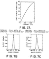
- a L-I characteristic and a beam divergence characteristic of the semiconductor optical device are exemplified.
- the semiconductor optical device is coated with a multi-film whim has a reflection rate of 95 % at the rear facet after cleaving a resonator length to 250 ⁇ m.
- a threshold current is equal to 6.0 mA at 25°C
- a slope efficiency is equal to 0.56 W/A
- full width at half maximum of the far-field pattern optical strength distribution is equal to 13.2° in the parallel direction and 15.4° in the vertical direction with respect to the narrow beam divergence characteristic.
- the width of each of the active layers of thirty devices which are taken out from arbitrary positions within radius 18 mm of three different wafer has an average value of 0.288 ⁇ m and a standard deviation of 0.018 ⁇ m at the forward facet, and the average value of 1.587 ⁇ m and the standard deviation of 0.022 ⁇ m at the rear facet, respectively.
- the semiconductor optical device is excessively superior in the uniformity and the reproducibility.
- Each of three hundred devices which are taken out in the same manner has the standard deviation of 0.52 mA of the threshold current at 25°C, the standard deviation of the slope efficiency of 0.041 W/A, the standard deviation of full width at half maximum of the fat-field pattern optical strength distribution of 0.5° in the parallel direction and 0.6° in the vertical direction.
- the semiconductor optical device has excessively excellent uniformity and the reproducibility.
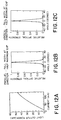
- the layer thickness and the band gap wavelength of the active layer consisting of the SCH layers 8a and 8b and the MQW layer 9 according to this example is kept constant in the resonator direction, as indicated by a solid line in Fig. 8A.
- the spot-size conversion efficiency is remarkably reduced as indicate by a dot line in Fig. 8A. This is because the thickness of the active layer which is selectively grown is increased as the opening portion becomes narrower. Further, the optical gain wavelength of the entire resonator is dispersed because the band gap wavelength becomes long. Consequently, the L-I characteristic of the semiconductor laser is largely degraded.
- the selective growth mask 2a of this example is designed to avoid the deterioration of the performance as the semiconductor laser having the narrow beam divergence. Consequently, the active layer thickness and the band gap wavelength are kept almost constant.
- an optimum value of the mask width Wm which is accompanied with the change of the opening width Wo is variable in accordance with the growth method and the growth condition of the semiconductor optical waveguide including the active layer in addition to the changing quantity of the opening width and the referential mask width. Therefore the dimension of the selective growth mask 2a is not limited to the above-mentioned value, and should be suitably determined by taking the characteristic of the optical waveguide, the growth method and the growth condition of the semiconductor layer into consideration.
- the layer thickness and the band gap composition become completely uniform in the optical waveguide direction, and it is possible that the band gap composition has a certain degree of distribution.
- the taper shape is not limited to the linear shape as illustrated in Fig. 6A, and the taper shape may have a gentle taper or the different taper length towards the forward facet, as shown in Figs. 9A and 9B.
- any shapes can be adopted as long as the optical waveguide includes the portion in which the mask width Wm and the opening width Wo gradually become smaller towards the facet.
- a semiconductor optical device according to a second example of this invention.
- the second example also corresponds to the first embodiment illustrated in Fig. 3.
- a SiO 2 film having the layer thickness of 0.05 ⁇ m is deposited by the use of the CVD method on an n-InP substrate 1a and is patterned by the use of the photo-lithography method and the dry-etching method to form a SiO 2 mask 2a.
- the mask width Wm and the opening width Wo of the mask 2a are set to 50.0 ⁇ m and 1.6 ⁇ m in the rear straight portion 4 having the length of 190 ⁇ m, respectively. Further, the mask width Wm and the opening width Wo gradually become smaller in the taper portion 5 having the length of 150 ⁇ m, and are set to 6.0 ⁇ m and 0.6 ⁇ m in the forward straight portion 6 having the length of 10 ⁇ m, respectively.
- an n-InP clad layer 7a (the thickness of 0.2 ⁇ m, the doping concentration of 1 ⁇ 10 18 cm -3 ), an n-type InGaAsP-SCH layer 8a (the PL wavelength of 1.13 ⁇ m composition, the thickness of 50 nm), a MQW layer 9 (the number of quantum well of seven, the PL wavelength of about 1.3 ⁇ m) consisting of an InGaAsP quantum well structure layer (the thickness of 5 nm) with +1.0% compressive strain and an InGaAsP barrier layer (the PL wavelength of 1.1 ⁇ m composition, the thickness of 8nm), a p-type InGa AsP-SCH layer 8b (the PL wavelength of 1.13 ⁇ m composition,the thickness of 50nm) and a p-InP clad layer 7b (the thickness of 0.1 ⁇ m, the doping concentration of 7 ⁇ 10 17 cm -3 ) are
- the layer thickness and the band gap wavelength of the active layer having the SCH layers 8a, 8b and the MQW layer 9 are illustrated in Fig. 11.
- the layer thickness of the optical waveguide is reduced in the taper portion 5 of the mask 2a and the band gap wavelength is shortened.
- the excellent spot-size conversion passive waveguide having a small optical absorb loss can be obtained in this example.
- a SiO 2 mask 10 having the opening width 1 ⁇ m for selectively growing a buried layer is formed on an n-InP substrate 1a by the use of the CVD method, the photo-lithography and the dry-etching method, as illustrated in Fig. 10C.
- a p-InP buried layer 12 and a p-InGaAs contact layer 13a are successively grown.
- an insulating film 15 is deposited, as illustrated in Fig. 10D.
- electrodes 14 are formed the upper and lower surfaces of the substrate 1a.
- the length of the opening which is formed in the insulating film 15 is equal to 220 ⁇ m at the total of 190 ⁇ m at the rear straight portion 4 and 30 ⁇ m at the rear side of the taper portion 5.
- a L-I characteristic and a beam divergence characteristic of the semiconductor optical device are indicated.
- the semiconductor optical device is coated with a multi-film which has a reflection rate of 95 % at a rear facet after cleaving a resonator length to 360 ⁇ m.
- the threshold current is equal to 8.0 mA at 25°C
- the slope efficiency is equal to 0.45 W/A
- the full width at half maximum of the far-field pattern image optical strength distribution is equal to 10.8° in the parallel direction and 10.6° in the vertical direction.
- the narrow beam divergence characteristic has an excellent aspect ratio.
- the width of each of the active layers of thirty devices which are taken out from arbitrary positions within radius 18mm of three different wafer has an average value of 0.224 ⁇ m and a standard deviation of 0.021 ⁇ m at the forward facet, and the average value of 1.177 ⁇ m and the standard deviation of 0.024 ⁇ m at the rear facet, respectively.
- the semiconductor optical device is excessively superior in the uniformity and the reproducibility.
- Each of three hundred devices which are taken out in the same manner has the standard deviation of 0.62 mA of the threshold current at 25°C, the standard deviation of the slope efficiency of 0.041 W/A, the standard deviation of the full width at half maximum of the far-field pattern optical strength distribution of 0.4° in the parallel and vertical directions.
- the semiconductor optical device has excessively excellent uniformity and the reproducibility.
- the full width at half maximum of the far-field pattern optical strength distribution of the spot-size conversion waveguide integration laser which has only the vertical direction taper and which is manufactured on the condition that the opening width Wo is constantly set to 1.6 ⁇ m at the design of the same mask width with this example is equal to 13° in the parallel and 15° in the vertical direction.
- a semiconductor optical device according to a third example of this invention.
- the third example corresponds to the second embodiment illustrated in Fig. 4.
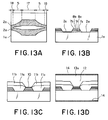
- a SiO 2 film having the layer thickness of 0.1 ⁇ m is deposited by the use of the CVD method on an n-InP substrate 1a and is patterned by the use of the photo-lithography method and the dry-etching method to form a SiO 2 mask 2a.
- the mask width Wm and the opening width Wo of the mask 2a are sat to 50.0 ⁇ m and 2.0 ⁇ m in the linear gain waveguide portion 17 having the length of 190 ⁇ m, respectively.
- the mask width Wm and the opening width Wo gradually become smaller in the taper portions 5 having the length of 130 ⁇ m, and are set to 1.0 ⁇ m and 0.6 ⁇ m in the portions which contact with the window structure portions 18 having the length of 10 ⁇ m, respectively.
- an n-InP clad layer 7a (the thickness of 0.2 ⁇ m, the doping concentration of 1 ⁇ 10 18 cm -3 ), an n-type InGaAsP-SCH layer 8a (the PL wavelength of 1.05 ⁇ m composition, the thickness of 50nm + the PL wavelength of 1.13 ⁇ m composition, the thickness of 10nm), a MQW layer 9 (the number of quantum well of six, the PL wavelength of about 1.3 ⁇ m) consisting of an InGaAsP quantum well structure layer (the thickness of 5nm) with +0.7% compressive strain and an InGaAsP barrier layer (the PL wavelength of 1.13 ⁇ m composition, the thickness of 8nm), a p-type InGa AsP-SCH layer 8b (the PL wavelength of 1.13 ⁇ m composition, the thickness or 10nm + the PL wavelength or 1.05 ⁇ m composition, the thickness of 50nm)
- SiO 2 mask 2a is removed, another SiO 2 mask 10 is formed only on the mesa type optical waveguide including the active layer by the use of the CVD method and the photo-lithography method, as illustrated in Fig. 13C.
- a current blocking structure consisting of a p-InP blocking layer 11a (the thickness of 0.5 ⁇ m, the doping concentration of 3 ⁇ 10 17 cm -3 ) and an n-InP blocking layer 11b (the thickness of 0.7 ⁇ m, the doping concentration of 1 ⁇ 10 18 cm -3 ) is successively deposited.
- a p-InP embedding layer 12 and a p-InGaAs contact layer 13a are successively deposited, as illustrated in Fig. 13D.
- electrodes 14 are formed on upper and lower surfaces of the substrate 1a, and is cleaved to the device length of 450 ⁇ m.
- the semiconductor optical amplifier having the facet of the window structure is finally obtained, as illustrated in Fig. 13D.
- a semiconductor optical device according to a fourth example of this invention.
- the fourth example corresponds to the third embodiment illustrated in Fig. 5.
- a SiO 2 film having the layer thickness of 0.05 ⁇ m is deposited by the use of the CVD method on an n-InP substrate 1a and is patterned by the use of the photo-lithography method and the dry-etching method to form a SiO 2 mask 2a.
- the mask width Wm and the opening width Wo of the mask 2a are set to 50.0 ⁇ m and 2.0 ⁇ m in the DFB laser portion20 having the length of 180 ⁇ m, respectively.
- an n-InP clad layer 7a (the thickness of 0.2 ⁇ m, the doping concentration of 1 ⁇ 10 18 cm -3 ), an n-type InGaAsP-SCH layer 8a (the PL wavelength of 1.13 ⁇ m composition, the thickness of 50nm), a MQW layer 9 (the number of quantum well of seven, the PL wavelength of about 1.3 ⁇ m) consisting of an InGaAsP quantum well structure layer (the thickness of 5nm) with +1.0% compressive strain and an InGaAsP barrier layer (the PL wavelength of 1.1 ⁇ m composition, the thickness of 8 nm), a p-type InGaAsP-SCH layer 8b (the PL wavelength of 1.13 ⁇ m composition, the thickness of 50nm) and a p-InP clad layer 7b (the thickness of 0.1 ⁇ m, the doping concentration of 7 ⁇ 10 17 cm
- the layer thickness and band gap wavelength of the active layer which is combined with the electrical absorb type modulator portion 19, the SCH layers 8a, 8b and the MQW layer 9 in the taper portion 5 are equal to 160 nm and 1.27 ⁇ m, respectively.
- a diffraction grating (not shown) is formed on the p-InP clad layer 7b of the DFB laser portion 20
- another SiO 2 mask 10 for selectively growing a buried layer having the opening width of 1 ⁇ m is formed on the n-InP substrate 1a by the use of the CVD method, the photo-lithography method and the dry-etching method, as illustrated in Fig. 14C.
- a p-InP buried layer 12 and a p-InGaAs contact layer 13a are successively deposited on the substrate 1a, as illustrated in Fig. 14C.
- an insulating film 15 is deposited by the use of the CVD method, as shown in Fig. 14D.
- electrodes 14 are formed on upper and lower surfaces of the substrate 1a.
- the modulator integration DFB laser is completed in this example, as illustrated in Fig. 14.
- the DBR laser may be used.
- the oscillation wavelength is equal to 1.3 ⁇ m in the above embodiments.
- any wavelength band including, for example, a visible wavelength band, such as 1.55 ⁇ m, 1.65 ⁇ m, 0.98 ⁇ m and 0.68 ⁇ m, may be used.
- the MQW structure having the compressive strained quantum well layer is used in the above embodiments, the MQW structure having no distortion, a distortion compensation type MQW structure and a bulk active layer may be used.
- AlGaInAs/InP system, AlGaAs/GaAs system, AlGaInP/GaInP system may be used as the materials other than the InGaAsP/InP system in the above-mentioned embodiments.
- a buried structure having, for example, a semi-insulating Fe doped InP may be used instead of the pnpn type current block structure or the homo-embedding structure of the P-InP.
- the conductivity type of the substrate is not limited to the n-type in the above embodiment, and may be a p-type.
Landscapes
- Physics & Mathematics (AREA)
- Condensed Matter Physics & Semiconductors (AREA)
- General Physics & Mathematics (AREA)
- Electromagnetism (AREA)
- Optics & Photonics (AREA)
- Semiconductor Lasers (AREA)
Applications Claiming Priority (3)
| Application Number | Priority Date | Filing Date | Title |
|---|---|---|---|
| JP09114559A JP3104789B2 (ja) | 1997-05-02 | 1997-05-02 | 半導体光素子およびその製造方法 |
| JP114559/97 | 1997-05-02 | ||
| JP11455997 | 1997-05-02 |
Publications (2)
| Publication Number | Publication Date |
|---|---|
| EP0875968A2 true EP0875968A2 (fr) | 1998-11-04 |
| EP0875968A3 EP0875968A3 (fr) | 2001-05-23 |
Family
ID=14640848
Family Applications (1)
| Application Number | Title | Priority Date | Filing Date |
|---|---|---|---|
| EP98108072A Withdrawn EP0875968A3 (fr) | 1997-05-02 | 1998-05-04 | Dispositif optique à semiconducteur et méthode de fabrication |
Country Status (3)
| Country | Link |
|---|---|
| US (2) | US6219366B1 (fr) |
| EP (1) | EP0875968A3 (fr) |
| JP (1) | JP3104789B2 (fr) |
Cited By (6)
| Publication number | Priority date | Publication date | Assignee | Title |
|---|---|---|---|---|
| EP0827242A3 (fr) * | 1996-08-30 | 2000-04-12 | Sony Corporation | Laser à semi-conducteur |
| EP1017141A3 (fr) * | 1998-12-28 | 2000-11-15 | Nec Corporation | Module laser avec modulateur integré |
| WO2001057978A1 (fr) * | 2000-02-02 | 2001-08-09 | Infineon Technologies Ag | Diode laser comportant un guide d'ondes a moulure et une bande interieure effilee |
| WO2001029590A3 (fr) * | 1999-10-22 | 2001-12-20 | Sarnoff Corp | Expanseur de mode a reseau grave co-directionnel |
| GB2483283A (en) * | 2010-09-03 | 2012-03-07 | Oclaro Technology Ltd | Optoelectronic device with tapered waveguide |
| WO2021009006A1 (fr) * | 2019-07-12 | 2021-01-21 | Osram Opto Semiconductors Gmbh | Diode laser à semi-conducteur à émission par la tranche et procédé pour fabriquer une telle diode |
Families Citing this family (61)
| Publication number | Priority date | Publication date | Assignee | Title |
|---|---|---|---|---|
| JP3323844B2 (ja) * | 1999-01-18 | 2002-09-09 | キヤノン株式会社 | ジャイロ |
| JP2000216495A (ja) | 1999-01-26 | 2000-08-04 | Nec Corp | 半導体光素子の製造方法 |
| KR100433298B1 (ko) * | 1999-02-08 | 2004-05-27 | 삼성전자주식회사 | 스폿 사이즈 변환기가 집적된 반도체 광 증폭기의 제조 방법 |
| US6528337B1 (en) * | 1999-04-08 | 2003-03-04 | The Furukawa Electric Co., Ltd. | Process of producing semiconductor layer structure |
| US6665330B1 (en) | 1999-09-14 | 2003-12-16 | Canon Kabushiki Kaisha | Semiconductor device having a semiconductor ring laser with a circularly formed ridge optical waveguide |
| JP4570712B2 (ja) * | 1999-10-14 | 2010-10-27 | Okiセミコンダクタ株式会社 | 半導体導波路素子及びその製造方法 |
| KR100406865B1 (ko) * | 1999-11-04 | 2003-11-21 | 삼성전자주식회사 | 선택 영역 성장법을 이용한 2중 코아 스폿 사이즈 변환기및 그 제조방법 |
| JP2001159521A (ja) | 1999-12-01 | 2001-06-12 | Canon Inc | 角速度検出装置 |
| JP2001168467A (ja) * | 1999-12-14 | 2001-06-22 | Nec Corp | 半導体レーザの製造方法 |
| JP4471522B2 (ja) * | 2000-03-15 | 2010-06-02 | 浜松ホトニクス株式会社 | 集光部品並びにこれを用いた光源モジュール、レーザー装置及び光信号増幅装置 |
| JP3941334B2 (ja) * | 2000-04-20 | 2007-07-04 | 株式会社日立製作所 | 光伝送モジュールおよびそれを用いた光通信システム |
| JP2001358405A (ja) * | 2000-06-14 | 2001-12-26 | Nec Corp | 半導体レーザ装置及びその製造方法 |
| JP4585168B2 (ja) | 2000-07-05 | 2010-11-24 | 三菱電機株式会社 | 半導体レーザ装置 |
| KR100358133B1 (ko) * | 2000-12-30 | 2002-10-25 | 한국전자통신연구원 | 스트레인 분산 패드를 이용한 측면-테이퍼 도파로 제조방법과 이를 응용한 모드변환기 제조방법 및 그에 따른광소자 |
| KR100369329B1 (ko) * | 2001-03-05 | 2003-01-24 | 주식회사 케이티 | 무결함, 무반사의 스폿사이즈 변환기를 구비한 광소자의제조 방법 |
| JP4026334B2 (ja) * | 2001-07-30 | 2007-12-26 | 株式会社日立製作所 | 半導体レーザ、分布帰還型半導体レーザおよび波長可変半導体レーザ |
| JP3786054B2 (ja) * | 2001-09-07 | 2006-06-14 | 日本電気株式会社 | 半導体光素子および半導体レーザ |
| JP2003258383A (ja) * | 2001-12-27 | 2003-09-12 | Fuji Photo Film Co Ltd | 窒化ガリウム系半導体レーザ及び画像露光装置 |
| US6813432B2 (en) * | 2002-05-31 | 2004-11-02 | Intel Corporation | Method for producing vertical tapers in optical waveguides by over polishing |
| US6956983B2 (en) * | 2002-05-31 | 2005-10-18 | Intel Corporation | Epitaxial growth for waveguide tapering |
| US6989284B2 (en) * | 2002-05-31 | 2006-01-24 | Intel Corporation | Fabrication of a waveguide taper through ion implantation |
| US7120336B2 (en) * | 2002-08-29 | 2006-10-10 | Micron Technology, Inc. | Resonator for thermo optic device |
| US7006746B2 (en) * | 2002-08-29 | 2006-02-28 | Micron Technology, Inc. | Waveguide for thermo optic device |
| US7020365B2 (en) * | 2002-08-29 | 2006-03-28 | Micron Technology, Inc. | Resistive heater for thermo optic device |
| US7301979B2 (en) * | 2003-05-22 | 2007-11-27 | Matsushita Electric Industrial Co., Ltd. | Semiconductor laser |
| KR100520796B1 (ko) * | 2003-10-20 | 2005-10-13 | 한국전자통신연구원 | 평면 매립형 반도체 광 증폭기의 제작 방법 |
| US7037739B2 (en) * | 2004-01-06 | 2006-05-02 | Korea Institute Of Science And Technology | Fabrication method of an epilayer structure InGaAsP/InP ridge waveguide phase modulator with high phase modulation efficiency |
| US7440666B2 (en) * | 2004-02-25 | 2008-10-21 | Avago Technologies Fiber Ip (Singapore) Pte. Ltd. | Buried heterostucture device having integrated waveguide grating fabricated by single step MOCVD |
| US7184640B2 (en) * | 2004-02-25 | 2007-02-27 | Avago Technologies Fiber Ip (Singapore) Pte. Ltd. | Buried heterostructure device fabricated by single step MOCVD |
| JP4575013B2 (ja) * | 2004-03-29 | 2010-11-04 | 住友電気工業株式会社 | 光電子集積装置の製造方法 |
| JP2005286192A (ja) * | 2004-03-30 | 2005-10-13 | Sumitomo Electric Ind Ltd | 光集積素子 |
| JP2005286196A (ja) * | 2004-03-30 | 2005-10-13 | Sumitomo Electric Ind Ltd | 光集積素子 |
| KR100651477B1 (ko) | 2005-01-19 | 2006-11-29 | 삼성전자주식회사 | 반도체 레이저와 반도체 레이저의 제작 방법 |
| KR100738530B1 (ko) * | 2005-07-21 | 2007-07-11 | 삼성전자주식회사 | 광 모드 변환기를 구비한 반도체 레이저 및 그 제조방법 |
| KR100759805B1 (ko) * | 2005-12-07 | 2007-09-20 | 한국전자통신연구원 | 광증폭 듀플렉서 |
| KR100754597B1 (ko) * | 2006-01-03 | 2007-09-05 | 삼성전자주식회사 | 광모드 크기 변환기 집적 레이저장치 및 그 제조방법 |
| JP4847176B2 (ja) * | 2006-03-29 | 2011-12-28 | 住友大阪セメント株式会社 | 光制御素子及びその製造方法 |
| US7573925B1 (en) | 2006-05-15 | 2009-08-11 | Finisar Corporation | Semiconductor laser having a doped active layer |
| US8277877B1 (en) | 2006-05-15 | 2012-10-02 | Finisar Corporation | Method for applying protective laser facet coatings |
| US7763485B1 (en) | 2006-05-15 | 2010-07-27 | Finisar Corporation | Laser facet pre-coating etch for controlling leakage current |
| US7606279B1 (en) | 2006-05-15 | 2009-10-20 | Finisar Corporation | Thin INP spacer layer in a high speed laser for reduced lateral current spreading |
| US8034648B1 (en) * | 2006-05-15 | 2011-10-11 | Finisar Corporation | Epitaxial regrowth in a distributed feedback laser |
| US7567601B1 (en) | 2006-05-15 | 2009-07-28 | Finisar Corporation | Semiconductor laser having low stress passivation layer |
| JP2008034614A (ja) * | 2006-07-28 | 2008-02-14 | Sharp Corp | 半導体レーザ素子およびその製造方法 |
| KR101374932B1 (ko) * | 2007-09-28 | 2014-03-17 | 재단법인서울대학교산학협력재단 | 확산 제한 식각과정에 의한 수평 변환 다공성 실리콘 광학필터의 제조방법 및 그에 의한 필터구조 |
| JP2009283605A (ja) * | 2008-05-21 | 2009-12-03 | Mitsubishi Electric Corp | 半導体レーザ |
| JP2010267871A (ja) * | 2009-05-15 | 2010-11-25 | Sony Corp | 半導体レーザおよびその製造方法 |
| JP4444368B1 (ja) | 2009-07-30 | 2010-03-31 | 古河電気工業株式会社 | 集積型半導体レーザ素子および半導体レーザモジュールならびに光伝送システム |
| TWI550900B (zh) * | 2009-09-16 | 2016-09-21 | 津湧科技股份有限公司 | 半導體元件層及其製造方法 |
| KR20130140736A (ko) * | 2010-11-22 | 2013-12-24 | 히타치가세이가부시끼가이샤 | 광도파로 |
| US9268089B2 (en) * | 2011-04-21 | 2016-02-23 | Octrolix Bv | Layer having a non-linear taper and method of fabrication |
| JP2017017112A (ja) * | 2015-06-29 | 2017-01-19 | 富士通株式会社 | 光半導体素子の製造方法 |
| CN106898948B (zh) * | 2015-12-17 | 2019-05-31 | 杭州增益光电科技有限公司 | 超辐射发光二极管或激光器外延结构及其制备方法 |
| DE102016113071A1 (de) * | 2016-07-15 | 2018-01-18 | Osram Opto Semiconductors Gmbh | Halbleiterlaserdiode |
| JP6146554B1 (ja) * | 2017-01-19 | 2017-06-14 | 三菱電機株式会社 | 光変調器集積半導体レーザ |
| US11245248B2 (en) * | 2018-01-10 | 2022-02-08 | Sony Semiconductor Solutions Corporation | Semiconductor laser |
| JP6537742B1 (ja) * | 2018-05-28 | 2019-07-03 | 三菱電機株式会社 | 半導体レーザ装置 |
| JP2021012990A (ja) * | 2019-07-09 | 2021-02-04 | 住友電気工業株式会社 | 量子カスケードレーザ |
| CN110233421B (zh) * | 2019-07-10 | 2020-08-04 | 中国工程物理研究院应用电子学研究所 | 一种基于环形外腔的锥形半导体激光器 |
| EP4037114B1 (fr) * | 2019-09-26 | 2024-05-01 | Nippon Telegraph And Telephone Corporation | Émetteur optique |
| US12596229B2 (en) * | 2022-08-12 | 2026-04-07 | Purdue Research Foundation | 3D tapered nanophotonic waveguide to fiber edge coupler |
Family Cites Families (29)
| Publication number | Priority date | Publication date | Assignee | Title |
|---|---|---|---|---|
| US5585957A (en) * | 1993-03-25 | 1996-12-17 | Nippon Telegraph And Telephone Corporation | Method for producing various semiconductor optical devices of differing optical characteristics |
| JP3548986B2 (ja) | 1994-02-15 | 2004-08-04 | 富士通株式会社 | 光半導体装置及びその製造方法 |
| EP0641049B1 (fr) * | 1993-08-31 | 1998-10-28 | Fujitsu Limited | Dispositif optique à semi-conducteur et sa méthode de fabrication |
| JP2682421B2 (ja) | 1993-12-28 | 1997-11-26 | 日本電気株式会社 | 半導体光集積回路の製造方法 |
| US5844929A (en) * | 1994-02-24 | 1998-12-01 | British Telecommunications Public Limited Company | Optical device with composite passive and tapered active waveguide regions |
| JP2937751B2 (ja) * | 1994-04-28 | 1999-08-23 | 日本電気株式会社 | 光半導体装置の製造方法 |
| JP2687891B2 (ja) | 1994-08-29 | 1997-12-08 | 日本電気株式会社 | 波長可変半導体レーザ |
| DE69505064T4 (de) | 1994-07-15 | 2000-02-24 | Nec Corp., Tokio/Tokyo | Wellenlängenabstimmbarer Halbleiterlaser |
| JP2842292B2 (ja) | 1994-09-16 | 1998-12-24 | 日本電気株式会社 | 半導体光集積装置および製造方法 |
| JPH08116135A (ja) | 1994-10-17 | 1996-05-07 | Mitsubishi Electric Corp | 導波路集積素子の製造方法,及び導波路集積素子 |
| JP2865000B2 (ja) * | 1994-10-27 | 1999-03-08 | 日本電気株式会社 | 出力導波路集積半導体レーザとその製造方法 |
| EP0720243A3 (fr) * | 1994-12-27 | 1998-07-01 | Fujitsu Limited | Procédé de fabrication de dispositif à semi-conducteur composé et dispositif optique à semi-conducteur |
| JPH08307012A (ja) * | 1995-05-01 | 1996-11-22 | Mitsubishi Electric Corp | 選択成長用マスク,半導体光装置の製造方法,および半導体光装置 |
| JPH08330673A (ja) * | 1995-06-02 | 1996-12-13 | Fujitsu Ltd | 光半導体装置 |
| JPH0923036A (ja) | 1995-07-05 | 1997-01-21 | Nippon Telegr & Teleph Corp <Ntt> | 半導体レーザ |
| US6198863B1 (en) * | 1995-10-06 | 2001-03-06 | British Telecommunications Public Limited Company | Optical filters |
| JPH1075011A (ja) * | 1996-08-30 | 1998-03-17 | Sony Corp | 半導体レーザ |
| US5870417A (en) * | 1996-12-20 | 1999-02-09 | Sdl, Inc. | Thermal compensators for waveguide DBR laser sources |
| JPH11112081A (ja) * | 1997-10-01 | 1999-04-23 | Mitsubishi Electric Corp | 半導体レーザ,及びその製造方法 |
| US6014396A (en) * | 1997-09-05 | 2000-01-11 | Sdl, Inc. | Flared semiconductor optoelectronic device |
| US6229947B1 (en) * | 1997-10-06 | 2001-05-08 | Sandia Corporation | Tapered rib fiber coupler for semiconductor optical devices |
| US6052397A (en) * | 1997-12-05 | 2000-04-18 | Sdl, Inc. | Laser diode device having a substantially circular light output beam and a method of forming a tapered section in a semiconductor device to provide for a reproducible mode profile of the output beam |
| US6381380B1 (en) * | 1998-06-24 | 2002-04-30 | The Trustees Of Princeton University | Twin waveguide based design for photonic integrated circuits |
| US6167073A (en) * | 1998-07-23 | 2000-12-26 | Wisconsin Alumni Research Foundation | High power laterally antiguided semiconductor light source with reduced transverse optical confinement |
| US6310995B1 (en) * | 1998-11-25 | 2001-10-30 | University Of Maryland | Resonantly coupled waveguides using a taper |
| US6162655A (en) * | 1999-01-11 | 2000-12-19 | Lucent Technologies Inc. | Method of fabricating an expanded beam optical waveguide device |
| US6445724B2 (en) * | 2000-02-23 | 2002-09-03 | Sarnoff Corporation | Master oscillator vertical emission laser |
| AU2001252891A1 (en) * | 2000-02-29 | 2001-09-12 | The Regents Of The University Of California | Ultra-compact room temperature rapidly tunable infrared sources |
| US6636547B2 (en) * | 2000-04-28 | 2003-10-21 | Photodigm, Inc. | Multiple grating-outcoupled surface-emitting lasers |
-
1997
- 1997-05-02 JP JP09114559A patent/JP3104789B2/ja not_active Expired - Fee Related
-
1998
- 1998-05-04 US US09/071,159 patent/US6219366B1/en not_active Expired - Fee Related
- 1998-05-04 EP EP98108072A patent/EP0875968A3/fr not_active Withdrawn
-
2001
- 2001-02-16 US US09/784,198 patent/US6465269B2/en not_active Expired - Fee Related
Cited By (7)
| Publication number | Priority date | Publication date | Assignee | Title |
|---|---|---|---|---|
| EP0827242A3 (fr) * | 1996-08-30 | 2000-04-12 | Sony Corporation | Laser à semi-conducteur |
| EP1017141A3 (fr) * | 1998-12-28 | 2000-11-15 | Nec Corporation | Module laser avec modulateur integré |
| WO2001029590A3 (fr) * | 1999-10-22 | 2001-12-20 | Sarnoff Corp | Expanseur de mode a reseau grave co-directionnel |
| WO2001057978A1 (fr) * | 2000-02-02 | 2001-08-09 | Infineon Technologies Ag | Diode laser comportant un guide d'ondes a moulure et une bande interieure effilee |
| GB2483283A (en) * | 2010-09-03 | 2012-03-07 | Oclaro Technology Ltd | Optoelectronic device with tapered waveguide |
| WO2021009006A1 (fr) * | 2019-07-12 | 2021-01-21 | Osram Opto Semiconductors Gmbh | Diode laser à semi-conducteur à émission par la tranche et procédé pour fabriquer une telle diode |
| US12407147B2 (en) | 2019-07-12 | 2025-09-02 | Osram Opto Semiconductors Gmbh | Edge-emitting semiconductor laser diode and method of manufacturing the same |
Also Published As
| Publication number | Publication date |
|---|---|
| JPH10308556A (ja) | 1998-11-17 |
| EP0875968A3 (fr) | 2001-05-23 |
| US6219366B1 (en) | 2001-04-17 |
| US6465269B2 (en) | 2002-10-15 |
| US20010010701A1 (en) | 2001-08-02 |
| JP3104789B2 (ja) | 2000-10-30 |
Similar Documents
| Publication | Publication Date | Title |
|---|---|---|
| US6465269B2 (en) | Semiconductor optical device and method of manufacturing the same | |
| EP0836255B1 (fr) | Réseau laser à diode et méthode de fabrication | |
| US5835261A (en) | Semiconductor optical amplifier device capable of deflecting output laser beam | |
| JPH07114308B2 (ja) | オプトエレクトロニクス半導体装置及びその製造方法 | |
| JPH0653619A (ja) | 化合物半導体装置及びその製造方法 | |
| US5636237A (en) | Semiconductor laser device which makes it possible to realize high-speed modulation | |
| US20020018503A1 (en) | Semiconductor device and manufacturing method thereof | |
| US20090296766A1 (en) | Quantum dot laser diode and method of manufacturing the same | |
| US6661828B2 (en) | Semiconductor laser device | |
| JP2882335B2 (ja) | 光半導体装置およびその製造方法 | |
| JP3024611B2 (ja) | 半導体レーザおよびその製造方法 | |
| JP3548986B2 (ja) | 光半導体装置及びその製造方法 | |
| JP2007311522A (ja) | 半導体レーザ | |
| JP3390893B2 (ja) | 半導体レーザ装置 | |
| JP2002111125A (ja) | 分布帰還型半導体レーザ | |
| US6980577B1 (en) | Vertical laser cavity with a non-planar top mirror | |
| US7042921B2 (en) | Complex coupled single mode laser with dual active region | |
| JP2613975B2 (ja) | 周期利得型半導体レーザ素子 | |
| JP2555954B2 (ja) | 半導体レーザ | |
| JPH05299764A (ja) | 半導体レーザの製造方法 | |
| JP3479925B2 (ja) | 分布帰還型半導体レーザ及びその製造方法 | |
| KR20000053604A (ko) | 반도체광학장치 제조방법 | |
| JP2500615B2 (ja) | 埋め込み構造半導体光デバイスの製造方法 | |
| JPH11112096A (ja) | 半導体レーザ装置およびこれを用いた光通信システム | |
| US7564883B2 (en) | Optical semiconductor device and method for fabricating the same |
Legal Events
| Date | Code | Title | Description |
|---|---|---|---|
| PUAI | Public reference made under article 153(3) epc to a published international application that has entered the european phase |
Free format text: ORIGINAL CODE: 0009012 |
|
| AK | Designated contracting states |
Kind code of ref document: A2 Designated state(s): DE FR NL |
|
| AX | Request for extension of the european patent |
Free format text: AL;LT;LV;MK;RO;SI |
|
| PUAL | Search report despatched |
Free format text: ORIGINAL CODE: 0009013 |
|
| AK | Designated contracting states |
Kind code of ref document: A3 Designated state(s): AT BE CH CY DE DK ES FI FR GB GR IE IT LI LU MC NL PT SE |
|
| AX | Request for extension of the european patent |
Free format text: AL;LT;LV;MK;RO;SI |
|
| RIC1 | Information provided on ipc code assigned before grant |
Free format text: 7H 01S 3/085 A, 7H 01S 3/19 B, 7H 01L 33/00 B, 7H 01S 5/026 B |
|
| 17P | Request for examination filed |
Effective date: 20010417 |
|
| AKX | Designation fees paid |
Free format text: DE FR NL |
|
| 17Q | First examination report despatched |
Effective date: 20020225 |
|
| STAA | Information on the status of an ep patent application or granted ep patent |
Free format text: STATUS: THE APPLICATION IS DEEMED TO BE WITHDRAWN |
|
| 18D | Application deemed to be withdrawn |
Effective date: 20020910 |