EP0877227A2 - Mikromechanischer Schwingstabkreisel - Google Patents
Mikromechanischer Schwingstabkreisel Download PDFInfo
- Publication number
- EP0877227A2 EP0877227A2 EP98107953A EP98107953A EP0877227A2 EP 0877227 A2 EP0877227 A2 EP 0877227A2 EP 98107953 A EP98107953 A EP 98107953A EP 98107953 A EP98107953 A EP 98107953A EP 0877227 A2 EP0877227 A2 EP 0877227A2
- Authority
- EP
- European Patent Office
- Prior art keywords
- layer
- layers
- group
- rotation sensor
- rotation
- Prior art date
- Legal status (The legal status is an assumption and is not a legal conclusion. Google has not performed a legal analysis and makes no representation as to the accuracy of the status listed.)
- Ceased
Links
Images

Classifications
-
- G—PHYSICS
- G01—MEASURING; TESTING
- G01C—MEASURING DISTANCES, LEVELS OR BEARINGS; SURVEYING; NAVIGATION; GYROSCOPIC INSTRUMENTS; PHOTOGRAMMETRY OR VIDEOGRAMMETRY
- G01C19/00—Gyroscopes; Turn-sensitive devices using vibrating masses; Turn-sensitive devices without moving masses; Measuring angular rate using gyroscopic effects
- G01C19/56—Turn-sensitive devices using vibrating masses, e.g. vibratory angular rate sensors based on Coriolis forces
- G01C19/5642—Turn-sensitive devices using vibrating masses, e.g. vibratory angular rate sensors based on Coriolis forces using vibrating bars or beams
- G01C19/5656—Turn-sensitive devices using vibrating masses, e.g. vibratory angular rate sensors based on Coriolis forces using vibrating bars or beams the devices involving a micromechanical structure
Definitions
- This invention relates to the field of gyroscopes and rotation sensors, and more particularly to rotation sensors that utilize an oscillating mechanical element to sense rotation in a single plane.
- One prior art method of sensing rotation and rotation rate utilizes a vibrating mechanical element in which the Coriolis force that arises when the element is rotated is used to measure rotation rate.
- Devices of this type include the hemispherical resonator gyroscope and the vibrating ring gyroscope.
- Such vibratory gyroscopes have no rotating parts and are easily miniaturized using known micro-machining techniques. However, these gyroscopes tend to be very expensive.
- Another method utilizes a rotation sensor based on a vibrating mechanical element, preferably a cantilever micro-beam, induced to laterally oscillate.
- a vibrating mechanical element preferably a cantilever micro-beam
- Such micro-beams are coupled directly to a stationary mounting structure.
- the vibration amplitude is measured by sensing the change in electrical capacitance between the moving beam and its stationary mounting structure.
- the magnitude of capacitance change is commonly on the order of femptofarads.
- the present invention provides such a device along with compatibility with external breadboard electronics which, together with the relative simplicity of its electronics, eliminates the complex electronics, manufacture, and associated costs attendant with the prior art devices.
- the present invention seeks to provide a low cost, long life, rotation sensor suitable for use in various applications in aircraft, spacecraft and the like.
- the rotation sensor is based on an oscillating mechanical element, preferably a cantilevered micro-beam, that is mounted to a substrate base at one end and free to vibrate at the other end.
- the beam is positioned in the X-Y plane and is induced to oscillate along the Z-axis, i.e., "perpendicular" thereto.
- the cantilevered beam is fabricated using photolithographic techniques in five layers formed along the longitudinal axis of the beam.
- the beam incorporates three layers of conducting (or semi-conducting) material forming top and bottom outer layers and an inner layer. Each outer layer of conducting material is separated from the middle layer of conducting material by a layer of insulating material.
- the middle conductive layer may be thicker than the outer conductive layers in order to provide the principal mechanical element of the beam.
- a conductive end plate is fabricated across the free end of the beam, electrically connecting the three conductive layers.
- the bottom outer conductive layer is formed on a substrate at the beam's fixed end.
- the substrate and the connected outer conductive layer are at electrical ground and the remaining outer conductive layer is connected, at the fixed end of the beam, to a DC voltage source.
- the middle conductive layer is connected at the fixed end of the beam to an AC-coupled amplifier.
- a DC voltage is applied between the two outer conductive layers at the fixed end of the beam and the voltage at he middle conducting layer adjacent the beam's fixed end is capacitively coupled into the amplifier.
- the peak-to-peak AC voltage output at the center layer is in equilibrium.
- the "strain gauge” effect is altered resulting in a change to the peak-to-peak AC voltage at the middle layer. This change in the peak-to-peak AC voltage is indicative of the direction and rate of rotation of the substrate.
- One of the advantages of the present inventive sensor is the simplicity of the associated electronics. Another primary advantage is its low impedance. The low impedance eliminates the requirement to co-locate the associated electronics on the same micro-chip as the micro-beam. Also, this is significant during the development phase of the sensor (micro-gyro) because it facilitates use of breadboard electronics external to the package containing the beam. Once the electronic circuit is fully developed and tested, it can be integrated into the same package if desired.
- micro-beam 10 the rotation sensor of the present invention is referred to generally as micro-beam 10.
- the invention is based on an oscillating mechanical element that is mounted to a substrate base at one end and free to vibrate at the other end.
- Beam 10 is positioned in the X-Y plane and has its longitudinal axis along the Y-axis. Beam 10 is induced to oscillate along the Z-axis, i.e., "perpendicular" thereto as shown by the up-down directional arrow.
- the cantilevered beam 10 is fabricated using well-known photolithographic techniques in five layers (12, 14, 16, 18, 20) formed along the longitudinal axis of the beam.
- the invention incorporates three layers of conducting (or semi-conducting) material forming top and bottom outer conducting layers 12 and 16, respectively, and an inner conducting layer 14.
- the outer layers 12 and 16 of conducting material are separated from the middle layer 14 of conducting material by layers 18 and 20, of insulating material.
- the middle conductive layer 14 may be thicker than the outer conductive layers 12 and 16 in order to provide the principal mechanical element of the beam 10.
- a conductive end plate 17 is fabricated across the free end of the beam 10 and electrically connects the three conductive layers 12,14,16.
- the bottom conductive layer 16 is formed on a substrate 22 at one end of beam 10 preventing movement of that end, except with respect to movement of the substrate 22.
- the substrate 22 and the connected bottom conductive layer 16 are connected at electrical connection pad 28 to electrical ground 32 and top conductive layer 12 is connected, at electrical connection 24 to a DC voltage source 30.
- the middle conductive layer 14 is connected at electrical pad 26 through a capacitor 34 to a high gain amplifier 36.
- a DC voltage is applied between the outer conductive layers 12 and 16 through connections 24 and 28.
- the voltage at connector 26 on the middle conducting layer 14 is capacitively coupled via capacitor 34 into the amplifier 36.
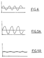
- the peak-to-peak AC voltage output at middle layer 14 is held at a peak-to-peak amplitude level dependent upon the conductive material used in the layers 12,14,16 and the value of DC voltage impressed across layers 12 and 16.
- a representative signal waveform depicting this condition is shown in Fig. 4.
- beam 10 is moved in the direction of rotation, either up or down as shown by the up-down arrow of Fig. 1. This results in the "strain gauge" effect being altered resulting in a change to the peak-to-peak AC voltage at the middle layer 14.
- Figs. 5a & b there is shown the changes in the peak-to-peak AC voltage indicative of the direction and rate of rotation of the substrate 22.
- the increase and decrease of voltage on middle conducting layer 14 produces AC voltages having determinable peak-to-peak amplitudes equal in the positive and negative transitions.
- the direction of rotation will cause the amplitude of the AC signal coupled into amplifier 36 to increase or decrease depending upon the direction of rotation of the substrate, producing an output signal from amplifier 36 proportional to the amount of rotation.
- middle conducting layer 14 can be AC coupled to high-gain amplifier 36. Further, as the micro-beam 10 acts as a voltage divider having only very low resistances, the signal on middle conducting layer 14 is not attenuated by stray capacitance on the connection 26 between middle conducting layer 14 and amplifier 36 so that amplifier 36 need not be co-located on the same substrate as micro-beam 10.
- the invention relates to a cantilevered micro-beam 10 formed on a micro-conduit substrate 22 such that when beam 10 is vibrated it produces an output signal directly related to rotation of the substrate 22 about an axis perpendicular to the beam 10 and the direction of vibration.
Landscapes
- Physics & Mathematics (AREA)
- Engineering & Computer Science (AREA)
- General Physics & Mathematics (AREA)
- Radar, Positioning & Navigation (AREA)
- Remote Sensing (AREA)
- Gyroscopes (AREA)
Applications Claiming Priority (2)
| Application Number | Priority Date | Filing Date | Title |
|---|---|---|---|
| US08/851,039 US5952573A (en) | 1997-05-05 | 1997-05-05 | Micro-beam motion sensor |
| US851039 | 1997-05-05 |
Publications (2)
| Publication Number | Publication Date |
|---|---|
| EP0877227A2 true EP0877227A2 (de) | 1998-11-11 |
| EP0877227A3 EP0877227A3 (de) | 2000-04-12 |
Family
ID=25309804
Family Applications (1)
| Application Number | Title | Priority Date | Filing Date |
|---|---|---|---|
| EP98107953A Ceased EP0877227A3 (de) | 1997-05-05 | 1998-04-30 | Mikromechanischer Schwingstabkreisel |
Country Status (3)
| Country | Link |
|---|---|
| US (1) | US5952573A (de) |
| EP (1) | EP0877227A3 (de) |
| JP (1) | JPH1144543A (de) |
Families Citing this family (1)
| Publication number | Priority date | Publication date | Assignee | Title |
|---|---|---|---|---|
| US6869010B2 (en) * | 2001-12-28 | 2005-03-22 | Xerox Corporation | In-line automated dual or selective multi-hole punch |
Family Cites Families (5)
| Publication number | Priority date | Publication date | Assignee | Title |
|---|---|---|---|---|
| US4381672A (en) * | 1981-03-04 | 1983-05-03 | The Bendix Corporation | Vibrating beam rotation sensor |
| US5802684A (en) * | 1993-09-14 | 1998-09-08 | Nikon Corporation | Process for producing a vibration angular-velocity sensor |
| US5596194A (en) * | 1994-08-19 | 1997-01-21 | Hughes Aircraft Company | Single-wafer tunneling sensor and low-cost IC manufacturing method |
| JP3399660B2 (ja) * | 1994-10-06 | 2003-04-21 | 株式会社東海理化電機製作所 | 表面型の加速度センサの製造方法 |
| JPH08201425A (ja) * | 1995-01-30 | 1996-08-09 | Mitsubishi Electric Corp | 半導体加速度検出装置 |
-
1997
- 1997-05-05 US US08/851,039 patent/US5952573A/en not_active Expired - Lifetime
-
1998
- 1998-04-30 EP EP98107953A patent/EP0877227A3/de not_active Ceased
- 1998-05-06 JP JP10123675A patent/JPH1144543A/ja active Pending
Also Published As
| Publication number | Publication date |
|---|---|
| EP0877227A3 (de) | 2000-04-12 |
| JPH1144543A (ja) | 1999-02-16 |
| US5952573A (en) | 1999-09-14 |
Similar Documents
| Publication | Publication Date | Title |
|---|---|---|
| US6155115A (en) | Vibratory angular rate sensor | |
| US6109105A (en) | Tunneling-based rate gyros with simple drive and sense axis coupling | |
| US4381672A (en) | Vibrating beam rotation sensor | |
| US6918298B2 (en) | Horizontal and tuning fork vibratory microgyroscope | |
| US6510745B2 (en) | Coriolis effect transducer | |
| US6550329B2 (en) | High Q angular rate sensing gyroscope | |
| JP4577671B2 (ja) | 角速度測定のための構成 | |
| US6089089A (en) | Multi-element micro gyro | |
| EP0323709B1 (de) | Dreiachsenbeschleunigungsmesser | |
| CN1886669B (zh) | 共振磁强计设备 | |
| JPH0769230B2 (ja) | 振動ビーム力トランスデューサ | |
| WO1998037380A1 (en) | Tuning fork gyro with split electrode | |
| US4267731A (en) | Force balanced vibratory rate sensor | |
| US6557415B2 (en) | Counterbalanced silicon tuned multiple accelerometer-gyro | |
| JP3130289B2 (ja) | タッチ信号プローブ | |
| US5952573A (en) | Micro-beam motion sensor | |
| WO1989010567A1 (en) | Accelerometer | |
| RU2018133C1 (ru) | Датчик инерциальной первичной информации | |
| US5092173A (en) | Secondary accelerometer pickoff | |
| EP0563762B1 (de) | Schwingkreisel mit Piezoelementen in Schwingungsknotennähe | |
| JP2535396B2 (ja) | 角速度測定装置 | |
| EP0426662B1 (de) | Messeinrichtung für winkelgeschwindigkeit | |
| JPH05133755A (ja) | 診断機能付振動ジヤイロ | |
| JPH0341312A (ja) | 角速度センサ及び角速度検出装置 |
Legal Events
| Date | Code | Title | Description |
|---|---|---|---|
| PUAI | Public reference made under article 153(3) epc to a published international application that has entered the european phase |
Free format text: ORIGINAL CODE: 0009012 |
|
| AK | Designated contracting states |
Kind code of ref document: A2 Designated state(s): DE FR GB |
|
| AX | Request for extension of the european patent |
Free format text: AL;LT;LV;MK;RO;SI |
|
| PUAL | Search report despatched |
Free format text: ORIGINAL CODE: 0009013 |
|
| AK | Designated contracting states |
Kind code of ref document: A3 Designated state(s): AT BE CH CY DE DK ES FI FR GB GR IE IT LI LU MC NL PT SE |
|
| AX | Request for extension of the european patent |
Free format text: AL;LT;LV;MK;RO;SI |
|
| RIC1 | Information provided on ipc code assigned before grant |
Free format text: 7G 01C 19/56 A, 7G 01P 13/02 B |
|
| 17P | Request for examination filed |
Effective date: 20001005 |
|
| AKX | Designation fees paid |
Free format text: DE FR GB |
|
| 17Q | First examination report despatched |
Effective date: 20041025 |
|
| STAA | Information on the status of an ep patent application or granted ep patent |
Free format text: STATUS: THE APPLICATION HAS BEEN REFUSED |
|
| 18R | Application refused |
Effective date: 20051210 |