EP0877437A1 - Résonateur du type ligne à bande et résonateur variable - Google Patents
Résonateur du type ligne à bande et résonateur variable Download PDFInfo
- Publication number
- EP0877437A1 EP0877437A1 EP98108190A EP98108190A EP0877437A1 EP 0877437 A1 EP0877437 A1 EP 0877437A1 EP 98108190 A EP98108190 A EP 98108190A EP 98108190 A EP98108190 A EP 98108190A EP 0877437 A1 EP0877437 A1 EP 0877437A1
- Authority
- EP
- European Patent Office
- Prior art keywords
- resonator
- transmission line
- conductors
- strip
- variable
- Prior art date
- Legal status (The legal status is an assumption and is not a legal conclusion. Google has not performed a legal analysis and makes no representation as to the accuracy of the status listed.)
- Withdrawn
Links
- 230000005540 biological transmission Effects 0.000 claims abstract description 89
- 239000004020 conductor Substances 0.000 claims abstract description 76
- 239000000758 substrate Substances 0.000 claims description 28
- 238000003475 lamination Methods 0.000 abstract description 11
- 230000001902 propagating effect Effects 0.000 abstract description 5
- 230000001681 protective effect Effects 0.000 abstract description 3
- 239000010410 layer Substances 0.000 description 50
- 239000003990 capacitor Substances 0.000 description 22
- 238000000034 method Methods 0.000 description 7
- 238000010586 diagram Methods 0.000 description 5
- 230000004907 flux Effects 0.000 description 5
- 101000869912 Cerastes vipera Disintegrin CV-11-alpha Proteins 0.000 description 4
- 230000008878 coupling Effects 0.000 description 4
- 238000010168 coupling process Methods 0.000 description 4
- 238000005859 coupling reaction Methods 0.000 description 4
- 230000000694 effects Effects 0.000 description 4
- VYPSYNLAJGMNEJ-UHFFFAOYSA-N Silicium dioxide Chemical compound O=[Si]=O VYPSYNLAJGMNEJ-UHFFFAOYSA-N 0.000 description 2
- QVQLCTNNEUAWMS-UHFFFAOYSA-N barium oxide Chemical compound [Ba]=O QVQLCTNNEUAWMS-UHFFFAOYSA-N 0.000 description 2
- 239000000919 ceramic Substances 0.000 description 2
- 238000002474 experimental method Methods 0.000 description 2
- 238000010030 laminating Methods 0.000 description 2
- 229910052763 palladium Inorganic materials 0.000 description 2
- 239000002356 single layer Substances 0.000 description 2
- 238000004544 sputter deposition Methods 0.000 description 2
- 238000001771 vacuum deposition Methods 0.000 description 2
- 239000011230 binding agent Substances 0.000 description 1
- 229910052802 copper Inorganic materials 0.000 description 1
- 238000004898 kneading Methods 0.000 description 1
- 238000010295 mobile communication Methods 0.000 description 1
- 230000010355 oscillation Effects 0.000 description 1
- TWNQGVIAIRXVLR-UHFFFAOYSA-N oxo(oxoalumanyloxy)alumane Chemical compound O=[Al]O[Al]=O TWNQGVIAIRXVLR-UHFFFAOYSA-N 0.000 description 1
- 239000000843 powder Substances 0.000 description 1
- 230000004044 response Effects 0.000 description 1
- 239000000377 silicon dioxide Substances 0.000 description 1
- 229910052709 silver Inorganic materials 0.000 description 1
Images




Classifications
-
- H—ELECTRICITY
- H01—ELECTRIC ELEMENTS
- H01P—WAVEGUIDES; RESONATORS, LINES, OR OTHER DEVICES OF THE WAVEGUIDE TYPE
- H01P7/00—Resonators of the waveguide type
- H01P7/08—Strip line resonators
- H01P7/084—Triplate line resonators
-
- H—ELECTRICITY
- H03—ELECTRONIC CIRCUITRY
- H03B—GENERATION OF OSCILLATIONS, DIRECTLY OR BY FREQUENCY-CHANGING, BY CIRCUITS EMPLOYING ACTIVE ELEMENTS WHICH OPERATE IN A NON-SWITCHING MANNER; GENERATION OF NOISE BY SUCH CIRCUITS
- H03B5/00—Generation of oscillations using amplifier with regenerative feedback from output to input
- H03B5/18—Generation of oscillations using amplifier with regenerative feedback from output to input with frequency-determining element comprising distributed inductance and capacitance
- H03B5/1841—Generation of oscillations using amplifier with regenerative feedback from output to input with frequency-determining element comprising distributed inductance and capacitance the frequency-determining element being a strip line resonator
- H03B5/1847—Generation of oscillations using amplifier with regenerative feedback from output to input with frequency-determining element comprising distributed inductance and capacitance the frequency-determining element being a strip line resonator the active element in the amplifier being a semiconductor device
Definitions
- the present invention relates to a strip-line resonator and, more particularly, to a strip-line resonator formed by laminating a plurality of dielectric layers.
- the present invention also relates to a variable resonator including the above strip-line resonator.
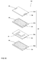
- FIG. 10 is an exploded perspective view of a conventional strip-line resonator.
- the strip-line resonator 50 includes a laminated body 51 comprising a third dielectric layer 52c having a single transmission line 51 of a single transmission line conductor thereon, a second and fourth dielectric layers 52b, 52d having respectively a ground conductor 53, and a first protective dielectric layer 52a, and formed is a ground terminal 54 which runs from the top surface to the bottom surface of the laminated body 51 along its side surface of the laminated body 51 and is electrically connected to the ground conductors 53.
- the third dielectric layer 52c having the transmission line 51 thereon is interposed between the second and fourth dielectric layers 52b, 52d, each having the ground conductor 53.
- the strip-line resonator 50 includes the single transmission line 51 of a single layer having a predetermined characteristic impedance between the two ground conductors 53.
- the strip-line resonator has the transmission line between the two ground conductors, and the effect of the stray capacity present between the transmission line and the ground electrodes lowers the characteristic impedance of the transmission line, thereby lowering Q factor.
- the present invention has been developed to overcome the above problem and to provide a compact strip-line resonator with a transmission line that heightens the characteristic impedance to a high impedance.
- the present invention provides a strip-line resonator, comprising: a laminated body including a plurality of dielectric layers laminated to each other; a plurality of transmission line conductors disposed between said dielectric layers respectively, in which at least two of said transmission line conductors are substantially opposed to each other via said dielectric layer and electrically connected in series so that high-frequency signals traveling on said transmission line conductors travel in the same direction; and a ground conductor disposed between said dielectric layers, opposed to said transmission line conductor via said dielectric layer, and electrically disconnected to said transmission line conductor.
- the transmission line includes a plurality of transmission line conductors, and the length of the transmission line conductor per layer is made shorter than in the conventional art, given that the characteristic impedance of the transmission line remains constant. As a result, a compact high-frequency component can be obtained.
- the transmission line is disposed between the two ground electrodes in a strip-line structure to shield transmission line from external electromagnetic noise, a drop in characteristic impedance of the transmission line arising from the effect of stray capacity generated between the transmission line and the ground electrodes is compensated for, and a high characteristic impedance of the transmission line is provided.
- the Q factor of the strip-line resonator is heightened.
- the present invention further provides a variable resonator including the above described strip-line resonator, comprising: a substrate including said strip-line resonator; a variable capacitance diode mounted on said substrate; a passive component disposed within or mounted on the substrate; and an external terminal provided on the surface of the substrate.
- variable resonator of the present invention Since in the variable resonator of the present invention, circuit components constituting the variable resonator are built into or mounted on a substrate which is a lamination of a plurality of dielectric layers, compact design is implemented in the variable resonator. As a result, the radio equipment incorporating the variable resonator is made compact accordingly.
- the resonator By building the resonator, constituting the variable resonator, into the substrate that is a lamination of a plurality of dielectric layers, the resonator is of a monolithic structure supported by the insulating supports, and is thus electrically insulated from outside.
- FIG. 1 is an exploded perspective view of a first embodiment of the strip-line resonator of the present invention.
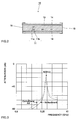
- FIG. 2 is a cross-sectional view of the strip-line resonator of FIG. 1.
- FIG. 3 is a Graph showing the resonance of the strip-line resonator of FIG. 1.
- FIG. 4 is a schematic diagram of the voltage-controlled oscillator that incorporates the strip-line resonator of FIG. 1.
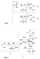
- FIG. 5 is a schematic diagram of a second embodiment of the variable resonator of the present invention.
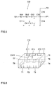
- FIG. 6 is a perspective view of the variable resonator of FIG. 5.
- FIGs. 7(a) ⁇ 7(f) are top views for the first ⁇ sixth dielectric layers constituting the substrate of the variable resonator of FIG. 6.
- FIGs. 8(a) ⁇ 8(d) are top views for the seventh ⁇ tenth dielectric layers constituting the substrate of the variable resonator of FIG. 6 and FIG. 8(e) is a bottom view of the tenth dielectric layer of the substrate.
- FIG. 9 is a schematic diagram of another embodiment of the variable resonator according to the present invention.
- FIG. 11 is a schematic diagram of the voltage-controlled oscillator employing a conventional variable resonator.
- FIG. 10 is an exploded perspective view showing one example of conventional strip-line resonator.
- FIGS. 1 and 2 are exploded perspective view and cross-sectional view of a first embodiment of the strip-line resonator of the present invention.
- the strip-line resonator 10 includes a lamination of a third dielectric layer 13c having a transmission line conductor 11a thereon and a via hole 12 in the direction of thickness, a fourth dielectric layer 13d having a transmission line conductor 11b thereon, a second and fifth dielectric layers 13b, 13e, each having a ground conductor 14 thereon, and a dielectric layer 13a for protective purpose.
- the transmission line conductors 11a, 11b respectively have a semi-spiral configuration, and face each other in the direction of lamination with the third dielectric layer 13a interposed therebetween such that both conductors are generally superimposed. Furthermore, the transmission line conductors 11a, 11b are electrically connected in series through the via hole 12 formed in the third dielectric layer 13c so that the directions of travel of high-frequency signals propagating on both conductors are the same, and both conductors constitute a single transmission line 11.
- the ground conductors 14 are arranged on the surfaces of the second and fifth dielectric layers 13b, 13e such that they respectively cover most of the surfaces of the second and fifth dielectric layers 13b, 13e.
- the transmission line conductors 11a, 11b and the ground conductors 14 are constructed of Ag, Pd, Ag-Pd, Cu or the like, and are formed on the surfaces of the second - fifth dielectric layers 13b - 13e using a known technique such as printing technique, sputtering technique, vacuum deposition technique.
- the first - fifth dielectric layers 13a - 13e is a sheet structure which is obtained by kneading a dielectric ceramic powder and a binder or the like.
- the first - fifth dielectric layers 13a - 13e thus constructed are laminated and sintered into a unitary body as a laminated body 13.
- the ground terminal 15 electrically connected to the ground conductors 14 runs from the top surface to the bottom surface of the laminated body 13 along the side surface of the laminated body 13.
- the ground terminal 15 is formed using sputtering technique, vacuum deposition technique, baking technique or the like.
- the strip-line resonator of the above embodiment comprises a single transmission line of two transmission line conductors between the two ground conductors, one top and one bottom, as shown in FIG. 2. Given a constant characteristic impedance, the length of the transmission line conductor per layer is approximately half that of the conventional art. As a result, compared with the conventional strip-line resonator (FIG. 5), the strip-line resonator of this embodiment assures the characteristic impedance of the transmission line to a predetermined value with its small-sized components, presenting a compact strip-line resonator.
- the directions of travel of high-frequency signals propagating on the two adjacent transmission line conductors with a dielectric layer interposed therebetween are the same, the directions of flow of the magnetic fluxes generated circularly around the transmission line conductors are the same.
- the two adjacent transmission line conductors with a dielectric layer interposed therebetween are electromagnetically coupled by the magnetic fluxes flowing circularly around them, and magnetic fluxes that flow circularly around the two adjacent transmission line conductors take place where the two adjacent transmission line conductors are closely stacked.
- the transmission line is disposed between the two ground electrodes to be a strip-line structure, a drop in characteristic impedance of the transmission line arising from the effect of stray capacity generated between the transmission line and the ground electrodes is compensated for, and a high characteristic impedance of the transmission line is provided.
- the Q factor of the strip-line resonator is heightened as shown in FIG. 3 (the solid line: this embodiment, the dotted line: conventional art).
- any strip-line resonator will fall within the scope of the present invention if its transmission line has a plurality of transmission line conductors which generally face one another in the direction of lamination of the laminated body with a dielectric layer therebetween and are electrically connected in series so that high-frequency signals on two adjacent transmission line conductors of the plurality of transmission line conductors travel in the same direction.
- the transmission line conductors have a semi-spiral configuration, and depending on the specifications about an available area and a desired characteristic impedance, the transmission line conductors may have a spiral configuration, a meandering configuration or a combination of both.
- FIG. 5 is a schematic diagram of a second embodiment of the variable resonator of the present invention.
- the variable resonator 110 comprises an input terminal 101, first and second ports P1 and P2, capacitors C11 ⁇ C15, resistors R11, R12, a variable capacitance diode CV11, and a resonator L11.
- the variable resonator 110 for example, constitutes a variable resonator X of a voltage-controlled oscillator shown in FIG. 10.
- the FIG. 10 shows a circuit arrangement of a voltage-controlled oscillator that is conventionally and widely used in a variety of radio equipment including mobile communications equipment such as a car phone and a portable telephone.
- a variable resonator X is constituted by the capacitors C51 ⁇ C53, the variable capacitance diode CV51, the resonator L51 and the inductor L52, and an active oscillator Y is constituted by capacitors C54 ⁇ C60, resistors R51 ⁇ R54, transistors Q51, Q52, and the inductor L53.
- the capacitance of the variable capacitance diode CV51 changes.
- the oscillation frequency is determined by the capacitance of the variable capacitance diode CV51 variably set by the input voltage VT and capacitance of the capacitors C52 ⁇ C53, and the resonator L51.
- FIG. 6 is a perspective view of the variable resonator 110 shown in FIG. 5.
- the variable resonator 110 includes a substrate 111 which is a lamination of a plurality of dielectric layers (not shown), and has, on one principal surface of the substrate 111, the variable capacitance diode CV11, the capacitance of which changes in response to an input voltage, and passive components including a capacitor C1 and resistors R1 and R2.
- the resonator L11 Disposed within the substrate 111 are the resonator L11, and capacitors C12 ⁇ C15 as passive components, though they are not shown.
- terminals T1 ⁇ T8 Formed on the other principal surface and side surfaces of the resonator L11 are terminals T1 ⁇ T8 such as interconnect terminals for connection with external components, an input terminal for receiving an input voltage, and a ground terminal for grounding.
- FIGS. 7(a) ⁇ 7(f) and FIGS. 8(a) ⁇ 8(d) are respectively top views and bottom views of dielectric layers constituting the substrate 111 of the variable resonator 110 of FIG. 6.
- the resonator L11 and capacitors C12 ⁇ C15, constituting the variable resonator 110, are contained in the substrate 111 and the substrate 111 is produced by laminating a first ⁇ tenth dielectric layers a ⁇ j from top to bottom, each constructed of low-temperature fired ceramic containing barium oxide, aluminum oxide, silica as its main components, which can be fired at a temperature range of 850°C ⁇ 1000°C.
- lands La1 ⁇ La5 for mounting the variable capacitance diode CV11, the capacitor C11 and the resistors R11, R12.
- Respectively formed on the second ⁇ fifth dielectric layers b ⁇ e are capacitor electrodes CC21, CC22, CC31, CC41, and CC51.
- transmission line conductors LL11 and LL12 constituting a transmission line L11.
- Formed on the underside of the ninth dielectric layer i are the input terminal 101, the first and second port P1, P2 and external terminals T1 ⁇ T8 serving as ground terminals.
- the first ⁇ tenth dielectric layers a ⁇ j have via holes VHa ⁇ VHi and signal line electrodes (not shown) in required locations, and by way of the via holes VHa ⁇ VHi, the capacitor electrodes CC21, CC22, CC31, CC41, CC51, the transmission line conductors LL11, LL12, the ground electrodes G11, G12, and the external terminals T1 ⁇ T8 are properly interconnected.
- the capacitors C12 ⁇ C15 of the variable resonator 110 are constructed between capacitor electrode CC21 and the capacitor electrode CC22, and between each of the capacitor electrodes CC31, CC41 and CC51 and the ground electrode G11, respectively.
- the resonator L11 is constructed of the transmission line constituted by the transmission line conductors LL11, LL12, and the ground electrodes G11, G12 disposed above and below them.
- the substrate 111 containing the resonator L11 and the capacitors C12 ⁇ C15, constituting the variable resonator 110 shown in FIG. 1, is thus constructed.
- the variable resonator 110 is constructed by mounting, on one principal surface of the substrate 111, the variable capacitance diode CV11, the capacitor C11, and the resistors R11, R12, constituting the variable resonator 10 shown in FIG. 5.
- the transmission line conductors LL11, LL12 constituting the resonator L11 are sandwiched between the sixth dielectric layer f and eighth dielectric layer h constituting the substrate 111, and are consequently sealed with the insulating supports.
- the capacitor C11 may be formed within the substrate in the same manner as the capacitors C12 ⁇ C15.
- the resistors R11, R12 may be formed on the principal surface of the substrate or within the substrate as a printed resistor.
- variable resonator of the present invention since in the variable resonator of the present invention, circuit components constituting the variable resonator, for example, the resonator, the variable capacitance diode, capacitors and resistors are built into or mounted on the substrate which is a lamination of a plurality of dielectric layers, compact design is implemented in the variable resonator. As a result, the radio equipment incorporating the variable resonator is made compact accordingly.
- the transmission line of the resonator in the variable resonator is constructed of a plurality of layers of transmission line conductors and the directions of travel of high-frequency signals propagating on two adjacent transmission line conductors with a dielectric layer placed therebetween are the same; thus, the directions of flows of the magnetic fluxes generated circularly around the transmission line conductors are the same. Therefore, by narrowing the spacing between two adjacent transmission line conductors, the coupling between the transmission line conductors of the resonator is increased.
- the coupling between the transmission line conductors of the resonator is increased and a desired characteristic impedance is easily obtained.
- the transmission line is disposed between the two ground electrodes to be a strip-line structure, a drop in characteristic impedance of the transmission line arising from the effect of stray capacity generated between the transmission line and the ground electrodes is compensated for, and a high characteristic impedance of the transmission line is provided. The Q factor of the resonator is thus heightened.
- the resonator By building the resonator into the substrate that is a lamination of a plurality of dielectric layers, the resonator is of a monolithic structure supported by the insulating supports, and is thus electrically insulated from outside.
- two variable resonators 120, 130 comprising an input terminal 121, a first ⁇ fourth ports P21 ⁇ P24, capacitors C21 ⁇ C29, resistors R21 ⁇ R23, variable capacitance diodes CV21, CV22, resonators L21, L22 may be integrated into a single substrate with the input terminal 121, capacitor C21 and resistor R21 common to both variable resonators.
- one variable resonator 120 is connected to a transmitter side voltage-controlled oscillator with the other variable resonator 130 connected to a receiver side voltage-controlled oscillator, the radio equipment having these mounted thereon is made even more compact.
- the transmission line constituting the resonator of the variable resonator shown in FIGS. 7 and 8 is one example and any resonator will fall within the scope of the present invention if its transmission line has a plurality of transmission line conductors which generally face one another in the direction of lamination of the laminated body with a dielectric layer therebetween and are electrically connected in series so that high-frequency signals on two adjacent transmission line conductors of the plurality of transmission line conductors travel in the same direction.
- the transmission line conductors have a semi-spiral configuration, and depending on the specifications about an available area and a desired characteristic impedance, the transmission line conductors may have a spiral configuration, a meandering configuration or a combination of both.
Landscapes
- Inductance-Capacitance Distribution Constants And Capacitance-Resistance Oscillators (AREA)
- Control Of Motors That Do Not Use Commutators (AREA)
Applications Claiming Priority (6)
| Application Number | Priority Date | Filing Date | Title |
|---|---|---|---|
| JP117252/97 | 1997-05-07 | ||
| JP11725297 | 1997-05-07 | ||
| JP263802/97 | 1997-09-29 | ||
| JP26380297 | 1997-09-29 | ||
| JP101151/98 | 1998-04-13 | ||
| JP10115198A JPH1127014A (ja) | 1997-05-07 | 1998-04-13 | 可変共振器 |
Publications (1)
| Publication Number | Publication Date |
|---|---|
| EP0877437A1 true EP0877437A1 (fr) | 1998-11-11 |
Family
ID=27309402
Family Applications (1)
| Application Number | Title | Priority Date | Filing Date |
|---|---|---|---|
| EP98108190A Withdrawn EP0877437A1 (fr) | 1997-05-07 | 1998-05-05 | Résonateur du type ligne à bande et résonateur variable |
Country Status (1)
| Country | Link |
|---|---|
| EP (1) | EP0877437A1 (fr) |
Cited By (4)
| Publication number | Priority date | Publication date | Assignee | Title |
|---|---|---|---|---|
| RU2170489C1 (ru) * | 2000-07-31 | 2001-07-10 | Московский государственный авиационный институт (технический университет) | Высокодобротный контур высокочастотного диапазона |
| WO2005122390A3 (fr) * | 2004-06-09 | 2006-12-14 | Epcos Ag | Oscillateur |
| CN1332476C (zh) * | 2003-04-24 | 2007-08-15 | 松下电器产业株式会社 | 高频谐振电路 |
| RU2356135C2 (ru) * | 2007-07-19 | 2009-05-20 | Союз участников рынка инфокоммуникационных услуг | Перестраиваемая малогабаритная высокотемпературная сверхпроводящая антенна |
Citations (5)
| Publication number | Priority date | Publication date | Assignee | Title |
|---|---|---|---|---|
| EP0519085A1 (fr) * | 1990-12-26 | 1992-12-23 | TDK Corporation | Dispositif pour radiofrequence |
| EP0590612A1 (fr) * | 1992-09-29 | 1994-04-06 | Matsushita Electric Industrial Co., Ltd. | Résonateur accordable en fréquence comprenant un varactor |
| US5404118A (en) * | 1992-07-27 | 1995-04-04 | Murata Manufacturing Co., Ltd. | Band pass filter with resonator having spiral electrodes formed of coil electrodes on plurality of dielectric layers |
| US5612656A (en) * | 1993-12-24 | 1997-03-18 | Murata Manufacturing Co., Ltd. | Resonator with spiral-shaped pattern electrodes |
| JPH0983219A (ja) * | 1995-09-07 | 1997-03-28 | Murata Mfg Co Ltd | ストリップライン共振器 |
-
1998
- 1998-05-05 EP EP98108190A patent/EP0877437A1/fr not_active Withdrawn
Patent Citations (5)
| Publication number | Priority date | Publication date | Assignee | Title |
|---|---|---|---|---|
| EP0519085A1 (fr) * | 1990-12-26 | 1992-12-23 | TDK Corporation | Dispositif pour radiofrequence |
| US5404118A (en) * | 1992-07-27 | 1995-04-04 | Murata Manufacturing Co., Ltd. | Band pass filter with resonator having spiral electrodes formed of coil electrodes on plurality of dielectric layers |
| EP0590612A1 (fr) * | 1992-09-29 | 1994-04-06 | Matsushita Electric Industrial Co., Ltd. | Résonateur accordable en fréquence comprenant un varactor |
| US5612656A (en) * | 1993-12-24 | 1997-03-18 | Murata Manufacturing Co., Ltd. | Resonator with spiral-shaped pattern electrodes |
| JPH0983219A (ja) * | 1995-09-07 | 1997-03-28 | Murata Mfg Co Ltd | ストリップライン共振器 |
Non-Patent Citations (1)
| Title |
|---|
| PATENT ABSTRACTS OF JAPAN vol. 97, no. 7 31 July 1997 (1997-07-31) * |
Cited By (4)
| Publication number | Priority date | Publication date | Assignee | Title |
|---|---|---|---|---|
| RU2170489C1 (ru) * | 2000-07-31 | 2001-07-10 | Московский государственный авиационный институт (технический университет) | Высокодобротный контур высокочастотного диапазона |
| CN1332476C (zh) * | 2003-04-24 | 2007-08-15 | 松下电器产业株式会社 | 高频谐振电路 |
| WO2005122390A3 (fr) * | 2004-06-09 | 2006-12-14 | Epcos Ag | Oscillateur |
| RU2356135C2 (ru) * | 2007-07-19 | 2009-05-20 | Союз участников рынка инфокоммуникационных услуг | Перестраиваемая малогабаритная высокотемпературная сверхпроводящая антенна |
Similar Documents
| Publication | Publication Date | Title |
|---|---|---|
| EP1215748B1 (fr) | Dispositif composite à hautes fréquences | |
| US6462628B2 (en) | Isolator device with built-in power amplifier and embedded substrate capacitor | |
| US7612634B2 (en) | High frequency module utilizing a plurality of parallel signal paths | |
| US6289204B1 (en) | Integration of a receiver front-end in multilayer ceramic integrated circuit technology | |
| JP6269846B2 (ja) | 複合部品およびフロントエンドモジュール | |
| US7443268B2 (en) | Bandpass filter within a multilayered low temperature co-fired ceramic substrate | |
| CN106716634A (zh) | 高频元器件 | |
| US5363067A (en) | Microstrip assembly | |
| JP3482090B2 (ja) | 積層型フィルタ | |
| JP4249595B2 (ja) | 高周波スイッチ回路及び高周波スイッチ部品 | |
| US7142067B2 (en) | Voltage-controlled oscillator, composite module, and communication apparatus | |
| JP2005210074A (ja) | 多層基板及びパワーアンプモジュール | |
| KR100636984B1 (ko) | 전압제어 발진기, 복합 모듈, 및 통신 장치 | |
| JP3650433B2 (ja) | アンテナスイッチ | |
| JPH07176913A (ja) | 誘電体共振器装置 | |
| JPH10335903A (ja) | 電圧制御通過帯域可変フィルタ、電圧制御共振周波数可変共振器およびそれらを用いる高周波回路モジュール | |
| JP2002111317A (ja) | 複数のフィルタを有する多層配線基板 | |
| JPH10276117A (ja) | 複合スイッチ回路部品 | |
| JP2002290186A (ja) | 低域通過フィルタ | |
| JP2003018040A (ja) | 高周波回路及びその高周波回路部品 | |
| JP4209850B2 (ja) | アンテナスイッチ | |
| JPH11261398A (ja) | 複合スイッチ回路及び複合スイッチ回路部品 | |
| JPH10190311A (ja) | 誘電体フィルタ | |
| JPH11274876A (ja) | ローパスフィルタおよび回路基板 | |
| JPH088450B2 (ja) | 電圧制御発振器 |
Legal Events
| Date | Code | Title | Description |
|---|---|---|---|
| PUAI | Public reference made under article 153(3) epc to a published international application that has entered the european phase |
Free format text: ORIGINAL CODE: 0009012 |
|
| 17P | Request for examination filed |
Effective date: 19980505 |
|
| AK | Designated contracting states |
Kind code of ref document: A1 Designated state(s): DE FI FR GB SE |
|
| AX | Request for extension of the european patent |
Free format text: AL;LT;LV;MK;RO;SI |
|
| AKX | Designation fees paid |
Free format text: DE FI FR GB SE |
|
| STAA | Information on the status of an ep patent application or granted ep patent |
Free format text: STATUS: THE APPLICATION HAS BEEN WITHDRAWN |
|
| 18W | Application withdrawn |
Withdrawal date: 20000306 |