EP0878265B1 - Lot, lötpaste und lötverfahren - Google Patents
Lot, lötpaste und lötverfahren Download PDFInfo
- Publication number
- EP0878265B1 EP0878265B1 EP96925127A EP96925127A EP0878265B1 EP 0878265 B1 EP0878265 B1 EP 0878265B1 EP 96925127 A EP96925127 A EP 96925127A EP 96925127 A EP96925127 A EP 96925127A EP 0878265 B1 EP0878265 B1 EP 0878265B1
- Authority
- EP
- European Patent Office
- Prior art keywords
- solder
- solder paste
- alloy
- soldering
- accordance
- Prior art date
- Legal status (The legal status is an assumption and is not a legal conclusion. Google has not performed a legal analysis and makes no representation as to the accuracy of the status listed.)
- Expired - Lifetime
Links
Images

Classifications
-
- B—PERFORMING OPERATIONS; TRANSPORTING
- B23—MACHINE TOOLS; METAL-WORKING NOT OTHERWISE PROVIDED FOR
- B23K—SOLDERING OR UNSOLDERING; WELDING; CLADDING OR PLATING BY SOLDERING OR WELDING; CUTTING BY APPLYING HEAT LOCALLY, e.g. FLAME CUTTING; WORKING BY LASER BEAM
- B23K35/00—Rods, electrodes, materials, or media, for use in soldering, welding, or cutting
- B23K35/22—Rods, electrodes, materials, or media, for use in soldering, welding, or cutting characterised by the composition or nature of the material
- B23K35/24—Selection of soldering or welding materials proper
- B23K35/26—Selection of soldering or welding materials proper with the principal constituent melting at less than 400°C
- B23K35/262—Sn as the principal constituent
-
- B—PERFORMING OPERATIONS; TRANSPORTING
- B23—MACHINE TOOLS; METAL-WORKING NOT OTHERWISE PROVIDED FOR
- B23K—SOLDERING OR UNSOLDERING; WELDING; CLADDING OR PLATING BY SOLDERING OR WELDING; CUTTING BY APPLYING HEAT LOCALLY, e.g. FLAME CUTTING; WORKING BY LASER BEAM
- B23K35/00—Rods, electrodes, materials, or media, for use in soldering, welding, or cutting
- B23K35/02—Rods, electrodes, materials, or media, for use in soldering, welding, or cutting characterised by mechanical features, e.g. shape
- B23K35/0222—Rods, electrodes, materials, or media, for use in soldering, welding, or cutting characterised by mechanical features, e.g. shape for use in soldering or brazing
- B23K35/0244—Powders, particles or spheres; Preforms made therefrom
- B23K35/025—Pastes, creams or slurries
Definitions
- the present invention relates to a solder, a solder paste and a soldering method used in soldering an electronic circuit board.
- Fig. 3 shows the microstructure of the conventional solder alloy and the microstructure at the bonding interface between the conventional solder material and a copper land.
- numeral 1 designates an ⁇ -solid solution with an Sn-rich phase.
- Numeral 2 designates a ⁇ -solid solution with a Pb-rich phase.
- Numeral 3 designates an intermetallic compound whose composition is Cu 3 Sn.
- Numeral 4 designates another intermetallic compound whose composition is Cu 6 Sn 5 .
- Numeral 5 designates a Cu land.
- the conventional solder as shown above used to be an eutectic alloy of Sn and Pb, which is composed of 63% by weight of Sn and 37% by weight of Pb and whose eutectic point is 183 °C.
- the alloy had a microstructure where the ⁇ -solid solution 1 and the ⁇ -solid solution 2 are in the lamellar state.
- the intermetallic compounds 4 and 5 were formed on the solder/copper land bonding interface.
- the conventional solder material had also another problem that since it has a lamellar structure in its alloy, the microstructure is thickened upon exposure to a high-temperature environment and a slip occurs on the microstructural interface of the solder upon application of a force on the solder, inducing crack development thereon. Moreover, the conventional solder material had still another problem that at soldering and under the high-temperature environment, double-layered hard and fragile intermetallic compounds will grow on the solder/copper land bonding interface, inducing crack development on the bonding interface.
- An aspect of the present invention is aimed at a provision of a solder which has been suppressed with respect to the growth of intermetallic compounds on the solder/copper land bonding interface and is excellent in the high temperature resistance.
- a further aspect of the present invention seeks to provide a solder paste using such solder, and a soldering method using the solder paste.
- the solder paste in accordance with the present invention may be composed of a powder of the above-mentioned solder and a flux.
- the flux is composed of at least rosin, an activator, a thixotropic agent and a solvent.
- the lead-free solder in accordance with the present invention whose essential component is Sn further includes 2.0 to 3.5 wt% of Ag, 5 to 18 wt% of Bi 0.1 - 0.7 Cu and optionally 0. 1 - 1.5% In.
- An addition of Cu suppresses the growth of intermetallic compounds on the solder/copper land bonding interface thereby improving the strength on the bonding interface.
- a Cu content below 0.1 wt% does not produce such effect for an alloy.
- the resultant alloy becomes hard and fragile. Accordingly, a preferred content of Cu is 0.1 to 0.7 wt%.
- the solder in accordance with the present invention optionally includes 0.1 to 1.5 wt% of In.
- the presence of In improves the expansion and the heat resistance such as resistance against thermal embrittleness of an alloy.
- a content of In below 0.1 wt% does not produce such effects for an alloy.
- the content is over 1.5 wt%, the resultant alloy has impaired mechanical strength. Accordingly, a preferred content of In is 0.1 to 1.5 wt%.
- the solder paste in accordance with the present invention may be prepared by adding a flux to a powder of the above-mentioned solder so as to make a paste.
- the flux is composed essentially of about 30 to 70 wt% of solids, such as rosin for imparting fluidity and viscosity to the paste, a small amount of an activator, a thixotropic agent for keeping the shape and a viscosity improver which is added if occasion demands, and about 70 to 30 wt% of a solvent.
- the flux used in the present invention is not limited to any particular one. Whether the reflow atmosphere is air or nitrogen atmosphere, fluxes of RA type with a relatively high activity and those fluxes of RMA type with a relatively low activity which require no rinsing are both suitable. It is preferable to use RMA type fluxes when the reflow atmosphere is air.
- soldering method in accordance with the present invention by a reflow soldering technique using the above-mentioned solder paste is characterized in that immediately after a passage of a soldering object with the solder paste through an area showing a peak temperature in a reflow furnace, it is cooled at a cooling rate of 10 °C/sec or more.
- the present invention melts the solder at a peak temperature of 240 to 250 °C of a reflow furnace. And, in solidifying the molten solder, rapid cooling as mentioned before suppresses the growth of intermetallic compounds such as Ag 3 Sn, Cu 3 Sn, Cu 6 Sn 5 and the like, and pulverizes and disperses Ag 3 Sn, thereby improving the mechanical strength and heat resistance at the joint.
- Table 1 lists the compositions of the solders in accordance with Examples 1 to 3 and Comparative Examples 1 and 2, and the characteristics of those solders. Example 1 is not part of the invention.
- solder pastes were prepared by mixing each of the powders of the respective solders (each mean particle size: about 30 to 40 ⁇ m) with the below-mentioned flux at a weight ratio of 9:1.
- a flux of the RMA type for use in air reflow which has the composition shown in Table 2 was used.
- Diphenylguanidine hydrobromide 1 wt% Thixotropic agent Caster oil 4 wt%
- Wettability was evaluated as follows. First, a certain amount of each of the above-mentioned solder pastes was printed on a copper plate. In an assumption that the solder paste thus printed has a real spherical shape on the copper plate, the diameter of the sphere is defined as D. Next, upon heating the copper plate to 240 °C, the solder paste is spread over the copper plate while wetting it. The height of the solder paste measured during this process is defined as H.
- the wettability of the solder paste is represented by 100 ⁇ (D-H)/D (%); the higher the value, the better the wettability.
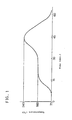
- the bonding strength was evaluated as follows. After printing each of the solder pastes on a board, an electronic part QFP (quad flat package) with a lead terminal pitch of 0.5 mm was mounted on the board using a placement equipment in order to adhere the QFP to the board by passing it through a reflow furnace having the reflow profile as shown in Fig. 1. The QFP and the board were preheated in the reflow furnace at 160 °C and immediately after they passed through an area showing a peak temperature of 240 °C, they were cooled at a cooling rate of 15 °C/sec using a blower. The lead terminal of the QFP which was adhered to the board in this way was hooked and pulled on at an angle of 45° to the board in order to measure the strength upon dissection of the lead terminal from the joint between the lead terminal and the board. The result represents the bonding strength.
- Thermal shock resistance was evaluated by the presence or absence of cracks on the joint after repeating 500 cycles of operation each comprising preliminary retention of a board to which an electronic part has been adhered in the aforementioned manner for 30 min at -40 °C, followed by retention for 5 min at room temperature and for 30 min at 80 °C, respectively.
- the solder in accordance with the present invention has a melting point of 220 °C or less which is suited for the reflow soldering technique, and thus it permits soldering at a temperature which does not injure electronic parts.
- the solder paste using the solder in accordance with the present invention shows satisfactory wettability to metallic copper, eliminating impairment of the bonding strength due to poor wettability.
- the joint finished with the reflow soldering technique using this solder paste is sufficiently strong and manifests excellent heat resistance, such as no crack development upon thermal shock test where a cold-hot retention cycle is repeated.
- Fig. 2 shows the microstructure of the solder alloy in accordance with the present invention at about 1,000 magnifications.
- Numeral 6 designates an intermetallic compound Ag 3 Sn which is a deposition in the alloy.
- the intermetallic compound shows a fine distribution in Fig. 2. This gives a joint which is less likely to change with time and manifests excellent heat resistance, such as resistance against thermal embrittleness, under high temperature environment.
- it is preferable in solidifying the solder to cool it at a cooling rate of 10 °C/sec or more. Cooling rates slower than that permit growth of intermetallic compound, making it impossible to have a fine alloy microstructure.
- the aforementioned cooling condition can be achieved by air cooling using a fan.
- solder which is free of a poisonous substance lead and excellent in both mechanical strength and heat resistance can be obtained.
- solder paste in accordance with the present invention is fit for reflow soldering, facilitating high density mounting of an electronic part.
Landscapes
- Engineering & Computer Science (AREA)
- Mechanical Engineering (AREA)
- Electric Connection Of Electric Components To Printed Circuits (AREA)
Claims (5)
- Lötmittel bestehend aus 2,0 bis 3,5 Gew.-% Ag, 5 bis 18 Gew.-% Bi, 0,1 bis 0,7 Gew-% Cu und gegebenenfalls 0,1 bis 1,5 Gew.-% In und abgesehen von Verunreinigungen SN als Rest.
- Lötmittelpaste, umfassend ein Flußmittel, zusammengesetzt aus wenigstens einem Harz, einem Aktivator, einem thixotropen Mittel und einem Lösungsmittel, zusammen mit einem Lötmittelpulver, worin das Lötmittel wie in Anspruch 1 definiert ist.
- Lötmittel oder Lötmittelpaste nach Anspruch 1 oder 2, das kein Blei enthält.
- Lötmittel oder Lötmittelpaste nach einem der vorhergehenden Ansprüche mit einem Schmelzpunkt von 220°C oder weniger.
- Lötverfahren mittels einer Aufschmelzlötungstechnik unter Verwendung der Lötmittelpaste nach einem der Ansprüche 2 bis 4, dadurch gekennzeichnet, daß direkt nach Durchgang eines Lötobjekts mit der Lötmittelpaste durch eine Fläche, welche eine Peaktemperatur in einem Schmelzofen zeigt, dieses mit einer Abkühlrate von 10°C/sek. oder mehr abgekühlt wird.
Applications Claiming Priority (4)
| Application Number | Priority Date | Filing Date | Title |
|---|---|---|---|
| JP2354796 | 1996-02-09 | ||
| JP23547/96 | 1996-02-09 | ||
| JP02354796A JP3220635B2 (ja) | 1996-02-09 | 1996-02-09 | はんだ合金及びクリームはんだ |
| PCT/JP1996/002138 WO1997028923A1 (en) | 1996-02-09 | 1996-07-29 | Solder, solder paste and soldering method |
Publications (3)
| Publication Number | Publication Date |
|---|---|
| EP0878265A1 EP0878265A1 (de) | 1998-11-18 |
| EP0878265A4 EP0878265A4 (de) | 1999-10-13 |
| EP0878265B1 true EP0878265B1 (de) | 2003-06-04 |
Family
ID=12113515
Family Applications (2)
| Application Number | Title | Priority Date | Filing Date |
|---|---|---|---|
| EP96925127A Expired - Lifetime EP0878265B1 (de) | 1996-02-09 | 1996-07-29 | Lot, lötpaste und lötverfahren |
| EP97101825A Expired - Lifetime EP0787559B1 (de) | 1996-02-09 | 1997-02-05 | Weichlotlegierung, Weichlotpaste und Verfahren zum Weichlöten |
Family Applications After (1)
| Application Number | Title | Priority Date | Filing Date |
|---|---|---|---|
| EP97101825A Expired - Lifetime EP0787559B1 (de) | 1996-02-09 | 1997-02-05 | Weichlotlegierung, Weichlotpaste und Verfahren zum Weichlöten |
Country Status (7)
| Country | Link |
|---|---|
| US (4) | US6267823B1 (de) |
| EP (2) | EP0878265B1 (de) |
| JP (1) | JP3220635B2 (de) |
| DE (2) | DE69628587T2 (de) |
| MY (1) | MY117994A (de) |
| SG (1) | SG43578A1 (de) |
| WO (1) | WO1997028923A1 (de) |
Families Citing this family (38)
| Publication number | Priority date | Publication date | Assignee | Title |
|---|---|---|---|---|
| US6184475B1 (en) * | 1994-09-29 | 2001-02-06 | Fujitsu Limited | Lead-free solder composition with Bi, In and Sn |
| US6371361B1 (en) * | 1996-02-09 | 2002-04-16 | Matsushita Electric Industrial Co., Ltd. | Soldering alloy, cream solder and soldering method |
| JP3220635B2 (ja) * | 1996-02-09 | 2001-10-22 | 松下電器産業株式会社 | はんだ合金及びクリームはんだ |
| JPH09326554A (ja) * | 1996-06-06 | 1997-12-16 | Matsushita Electric Ind Co Ltd | 電子部品接合用電極のはんだ合金及びはんだ付け方法 |
| EP0977900A4 (de) * | 1997-04-22 | 2001-06-13 | Ecosolder Internat Pty Ltd | Bleifreies lot |
| US6365097B1 (en) * | 1999-01-29 | 2002-04-02 | Fuji Electric Co., Ltd. | Solder alloy |
| GB9903552D0 (en) * | 1999-02-16 | 1999-04-07 | Multicore Solders Ltd | Reflow peak temperature reduction of solder alloys |
| JP4237325B2 (ja) | 1999-03-11 | 2009-03-11 | 株式会社東芝 | 半導体素子およびその製造方法 |
| JP3580731B2 (ja) | 1999-06-11 | 2004-10-27 | 和美 松重 | 鉛フリー半田の半田付け方法、及び当該半田付け方法にて半田付けされた接合体 |
| US6648216B2 (en) | 2000-08-21 | 2003-11-18 | Matsushita Electric Industrial Co., Ltd. | Process and apparatus for flow soldering |
| US6896172B2 (en) * | 2000-08-22 | 2005-05-24 | Senju Metal Industry Co., Ltd. | Lead-free solder paste for reflow soldering |
| US6433425B1 (en) | 2000-09-12 | 2002-08-13 | International Business Machines Corporation | Electronic package interconnect structure comprising lead-free solders |
| FR2818088B1 (fr) * | 2000-12-11 | 2003-02-28 | Air Liquide | Procede de realisation d'une brasure entre des billes metalliques d'un composant electronique et des plages d'accueil d'un circuit et four de brasage pour la mise en oeuvre de ce procede |
| EP1695382A4 (de) * | 2001-05-24 | 2007-10-10 | Fry Metals Inc | Thermisches grenzflächenmaterial und lot-preforms |
| CN1255563C (zh) * | 2001-05-24 | 2006-05-10 | 弗莱氏金属公司 | 热界面材料和受热器构型 |
| JP2003051671A (ja) * | 2001-06-01 | 2003-02-21 | Nec Corp | 実装構造体の製造方法および実装構造体 |
| US6541305B2 (en) * | 2001-06-27 | 2003-04-01 | International Business Machines Corporation | Single-melt enhanced reliability solder element interconnect |
| GB2380964B (en) | 2001-09-04 | 2005-01-12 | Multicore Solders Ltd | Lead-free solder paste |
| US6837947B2 (en) | 2002-01-15 | 2005-01-04 | National Cheng-Kung University | Lead-free solder |
| AU2003211032A1 (en) * | 2002-02-13 | 2003-09-04 | Honeywell International Inc. | Solder paste formulations, methods of production and uses thereof |
| US6805974B2 (en) * | 2002-02-15 | 2004-10-19 | International Business Machines Corporation | Lead-free tin-silver-copper alloy solder composition |
| JP3991788B2 (ja) * | 2002-07-04 | 2007-10-17 | 日本電気株式会社 | はんだおよびそれを用いた実装品 |
| DE10319888A1 (de) | 2003-04-25 | 2004-11-25 | Siemens Ag | Lotmaterial auf SnAgCu-Basis |
| US20060147337A1 (en) * | 2003-07-03 | 2006-07-06 | Antaya Technologies Corporation | Solder composition |
| US20050069725A1 (en) * | 2003-07-03 | 2005-03-31 | Boaz Premakaran T. | Lead-free solder composition for substrates |
| EP1724050B1 (de) * | 2004-03-09 | 2013-12-04 | Senju Metal Industry Co., Ltd. | Lötpaste |
| KR100797161B1 (ko) * | 2007-05-25 | 2008-01-23 | 한국생산기술연구원 | 주석-은-구리-인듐의 4원계 무연솔더 조성물 |
| CN102083583B (zh) * | 2007-07-23 | 2013-08-14 | 汉高有限公司 | 焊剂 |
| JP5058766B2 (ja) * | 2007-12-07 | 2012-10-24 | 山陽特殊製鋼株式会社 | 鉛フリー接合用材料を用いてはんだ付けしてなる電子機器 |
| JP2011138968A (ja) | 2009-12-28 | 2011-07-14 | Senju Metal Ind Co Ltd | 面実装部品のはんだ付け方法および面実装部品 |
| JP5724411B2 (ja) * | 2011-01-31 | 2015-05-27 | 富士通株式会社 | はんだ、はんだ付け方法及び半導体装置 |
| US9755229B2 (en) | 2011-06-14 | 2017-09-05 | Brookhaven Science Associates, Llc | Intermetallic M—Sn5 (M=Fe, Cu, Co, Ni) compound and a method of synthesis thereof |
| CN103212919A (zh) * | 2013-03-22 | 2013-07-24 | 宁波市鄞州品达电器焊料有限公司 | 一种改进的无铅焊锡丝及其助焊剂 |
| US11830672B2 (en) * | 2016-11-23 | 2023-11-28 | KYOCERA AVX Components Corporation | Ultracapacitor for use in a solder reflow process |
| CN106695161A (zh) * | 2016-12-29 | 2017-05-24 | 安徽华众焊业有限公司 | 一种锡铋合金的无铅焊料及其制备方法 |
| KR102058865B1 (ko) * | 2018-04-12 | 2019-12-24 | (주)아이엠 | 초가속 열소재를 이용한 발열 디바이스 및 이의 제조방법 |
| DE102020105180A1 (de) | 2020-02-27 | 2021-09-02 | Endress+Hauser SE+Co. KG | Verfahren zur Herstellung einer Lotverbindung, Verfahren zum Trennen zumindest eines Bauelements von einer Kontaktfläche, Leiterplatte und Feldgerät |
| DE102020128470A1 (de) | 2020-10-29 | 2022-05-05 | Endress+Hauser SE+Co. KG | Elektronisches Gerät und Verfahren zum Feststellen einer mechanischen Überbeanspruchung eines elektronischen Geräts |
Family Cites Families (41)
| Publication number | Priority date | Publication date | Assignee | Title |
|---|---|---|---|---|
| US16784A (en) * | 1857-03-10 | Improvement in casting plates for artificial teeth of alloys | ||
| CH80998A (fr) | 1918-08-09 | 1920-01-02 | Gustave Ferriere | Soudure pour l'aluminium |
| DE3730764C1 (de) | 1987-09-12 | 1988-07-14 | Demetron | Verwendung von Legierungen aus Zinn und/oder Blei als Weichlote zum Aufbringen von Halbleitern auf metallische Traeger |
| GB8807730D0 (en) * | 1988-03-31 | 1988-05-05 | Cookson Group Plc | Low toxicity soldering compositions |
| US5071058A (en) * | 1988-09-30 | 1991-12-10 | Union Carbide Industrial Gases Technology Corporation | Process for joining/coating using an atmosphere having a controlled oxidation capability |
| JPH04220192A (ja) * | 1990-12-14 | 1992-08-11 | Senju Metal Ind Co Ltd | 低残渣はんだペースト |
| JP2608995B2 (ja) * | 1991-02-12 | 1997-05-14 | 松下電器産業株式会社 | 光ビーム加熱半田用ソルダーペースト |
| GB9103018D0 (en) * | 1991-02-13 | 1991-03-27 | Lancashire Fittings Ltd | Lead free soft solder for stainless steel |
| JP3138486B2 (ja) | 1991-02-19 | 2001-02-26 | 株式会社タムラ製作所 | 伝熱リフローはんだ付け装置 |
| JPH04270062A (ja) | 1991-02-19 | 1992-09-25 | Tamura Seisakusho Co Ltd | 伝熱リフローはんだ付け装置 |
| JP3155778B2 (ja) | 1991-08-09 | 2001-04-16 | 山栄化学株式会社 | クリームはんだ |
| US5272007A (en) * | 1992-02-21 | 1993-12-21 | Union Carbide Chemicals & Plastics Technology Corporation | Solder powder coated with parylene |
| JP2722917B2 (ja) * | 1992-02-21 | 1998-03-09 | 松下電器産業株式会社 | 高温はんだ |
| JP2500018B2 (ja) * | 1992-08-24 | 1996-05-29 | 千住金属工業株式会社 | 低残渣はんだペ―スト |
| US5284074A (en) | 1992-12-14 | 1994-02-08 | Chen Ho T | Automatic screw-driving device |
| EP0612578A1 (de) * | 1993-02-22 | 1994-08-31 | AT&T Corp. | Gegenstand, der ein bleifreies Weichlot mit verbesserten mechanischen Eigenschaften enthält |
| US5389160A (en) | 1993-06-01 | 1995-02-14 | Motorola, Inc. | Tin bismuth solder paste, and method using paste to form connection having improved high temperature properties |
| JPH0825050B2 (ja) * | 1993-06-08 | 1996-03-13 | 日本アルミット株式会社 | 無含鉛半田合金 |
| US5411703A (en) | 1993-06-16 | 1995-05-02 | International Business Machines Corporation | Lead-free, tin, antimony, bismtuh, copper solder alloy |
| US5368814A (en) | 1993-06-16 | 1994-11-29 | International Business Machines, Inc. | Lead free, tin-bismuth solder alloys |
| US5328660A (en) | 1993-06-16 | 1994-07-12 | International Business Machines Corporation | Lead-free, high temperature, tin based multi-component solder |
| US5393489A (en) * | 1993-06-16 | 1995-02-28 | International Business Machines Corporation | High temperature, lead-free, tin based solder composition |
| JP3107483B2 (ja) | 1993-07-13 | 2000-11-06 | 日本アルミット株式会社 | 無ないし低含鉛半田合金 |
| JP3346848B2 (ja) * | 1993-08-11 | 2002-11-18 | 株式会社日本スペリア社 | 無鉛はんだ合金 |
| CA2131256A1 (en) * | 1993-09-07 | 1995-03-08 | Dongkai Shangguan | Lead-free solder alloy |
| US5439639A (en) | 1994-01-05 | 1995-08-08 | Sandia Corporation | Tin-silver-bismuth solders for electronics assembly |
| US5435857A (en) * | 1994-01-06 | 1995-07-25 | Qualitek International, Inc. | Soldering composition |
| US5415944A (en) * | 1994-05-02 | 1995-05-16 | Motorola, Inc. | Solder clad substrate |
| US5540379A (en) * | 1994-05-02 | 1996-07-30 | Motorola, Inc. | Soldering process |
| US5520752A (en) * | 1994-06-20 | 1996-05-28 | The United States Of America As Represented By The Secretary Of The Army | Composite solders |
| JPH08132277A (ja) * | 1994-11-01 | 1996-05-28 | Ishikawa Kinzoku Kk | 無鉛はんだ |
| JP3091098B2 (ja) * | 1994-11-01 | 2000-09-25 | 三井金属鉱業株式会社 | 熱交換器用はんだ合金 |
| JP2805595B2 (ja) * | 1994-11-02 | 1998-09-30 | 三井金属鉱業株式会社 | 鉛無含有半田合金 |
| US5429293A (en) * | 1994-12-19 | 1995-07-04 | Motorola, Inc. | Soldering process |
| US5593504A (en) * | 1995-04-26 | 1997-01-14 | Church & Dwight Co., Inc. | Method of cleaning solder pastes from a substrate with an aqueous cleaner |
| CA2221961C (en) * | 1995-05-24 | 2008-02-05 | Fry's Metals Inc. | Epoxy-based, voc-free soldering flux |
| KR970000429A (ko) * | 1995-06-30 | 1997-01-21 | 이형도 | 범용 무연땜납 |
| JP3220635B2 (ja) * | 1996-02-09 | 2001-10-22 | 松下電器産業株式会社 | はんだ合金及びクリームはんだ |
| US5730932A (en) * | 1996-03-06 | 1998-03-24 | International Business Machines Corporation | Lead-free, tin-based multi-component solder alloys |
| JPH09326554A (ja) * | 1996-06-06 | 1997-12-16 | Matsushita Electric Ind Co Ltd | 電子部品接合用電極のはんだ合金及びはんだ付け方法 |
| JP3369410B2 (ja) * | 1996-09-02 | 2003-01-20 | 松下電器産業株式会社 | 半導体装置の実装方法 |
-
1996
- 1996-02-09 JP JP02354796A patent/JP3220635B2/ja not_active Expired - Fee Related
- 1996-07-29 US US09/125,013 patent/US6267823B1/en not_active Expired - Fee Related
- 1996-07-29 DE DE69628587T patent/DE69628587T2/de not_active Expired - Fee Related
- 1996-07-29 EP EP96925127A patent/EP0878265B1/de not_active Expired - Lifetime
- 1996-07-29 WO PCT/JP1996/002138 patent/WO1997028923A1/ja not_active Ceased
-
1997
- 1997-01-31 US US08/792,128 patent/US5918795A/en not_active Expired - Fee Related
- 1997-02-04 MY MYPI97000413A patent/MY117994A/en unknown
- 1997-02-04 SG SG1997000248A patent/SG43578A1/en unknown
- 1997-02-05 DE DE69704725T patent/DE69704725T2/de not_active Expired - Fee Related
- 1997-02-05 EP EP97101825A patent/EP0787559B1/de not_active Expired - Lifetime
-
2001
- 2001-03-28 US US09/818,905 patent/US6428745B2/en not_active Expired - Lifetime
- 2001-05-16 US US09/855,553 patent/US20010025875A1/en not_active Abandoned
Also Published As
| Publication number | Publication date |
|---|---|
| US5918795A (en) | 1999-07-06 |
| EP0787559A1 (de) | 1997-08-06 |
| US20010018030A1 (en) | 2001-08-30 |
| MY117994A (en) | 2004-08-30 |
| US20010025875A1 (en) | 2001-10-04 |
| DE69704725D1 (de) | 2001-06-13 |
| DE69704725T2 (de) | 2001-08-23 |
| JPH09216089A (ja) | 1997-08-19 |
| EP0787559B1 (de) | 2001-05-09 |
| JP3220635B2 (ja) | 2001-10-22 |
| US6428745B2 (en) | 2002-08-06 |
| DE69628587D1 (de) | 2003-07-10 |
| EP0878265A4 (de) | 1999-10-13 |
| US6267823B1 (en) | 2001-07-31 |
| EP0878265A1 (de) | 1998-11-18 |
| SG43578A1 (en) | 1997-10-17 |
| WO1997028923A1 (en) | 1997-08-14 |
| DE69628587T2 (de) | 2004-04-29 |
Similar Documents
| Publication | Publication Date | Title |
|---|---|---|
| EP0878265B1 (de) | Lot, lötpaste und lötverfahren | |
| US6360939B1 (en) | Lead-free electrical solder and method of manufacturing | |
| US6554180B1 (en) | Lead-free solder paste | |
| JP3761678B2 (ja) | 錫含有鉛フリーはんだ合金及びそのクリームはんだ並びにその製造方法 | |
| EP2147740B1 (de) | Bleifreie Lötpaste | |
| JP4613823B2 (ja) | ソルダペーストおよびプリント基板 | |
| JP2003170294A (ja) | ソルダペースト | |
| US6159304A (en) | Solder paste | |
| JP3643008B2 (ja) | はんだ付け方法 | |
| KR101125865B1 (ko) | 솔더 페이스트, 이를 사용하여 형성된 솔더링 접합부, 및 상기 솔더링 접합부를 갖는 인쇄 회로 기판 | |
| KR100645241B1 (ko) | 혼합 합금 무연 솔더 페이스트 | |
| JPH09277082A (ja) | ソルダペースト | |
| JP3654161B2 (ja) | ソルダペーストとはんだ付け方法 | |
| EP1180411A1 (de) | Bleifreie Weichlotpaste zum Wiederaufschmelzlöten | |
| JPH09174278A (ja) | 無鉛はんだ合金およびそれを用いた電子回路装置 | |
| JPH0929480A (ja) | はんだペースト | |
| EP0931622B1 (de) | Lötpaste | |
| JP2021003730A (ja) | フラックス及びソルダペースト | |
| JPH0751889A (ja) | はんだ付け用フラックス | |
| JP2004058104A (ja) | はんだ付け用フラックス及びはんだペースト |
Legal Events
| Date | Code | Title | Description |
|---|---|---|---|
| PUAI | Public reference made under article 153(3) epc to a published international application that has entered the european phase |
Free format text: ORIGINAL CODE: 0009012 |
|
| 17P | Request for examination filed |
Effective date: 19980907 |
|
| AK | Designated contracting states |
Kind code of ref document: A1 Designated state(s): DE FR GB SE |
|
| A4 | Supplementary search report drawn up and despatched |
Effective date: 19990827 |
|
| AK | Designated contracting states |
Kind code of ref document: A4 Designated state(s): DE FR GB SE |
|
| 17Q | First examination report despatched |
Effective date: 20001201 |
|
| GRAG | Despatch of communication of intention to grant |
Free format text: ORIGINAL CODE: EPIDOS AGRA |
|
| GRAG | Despatch of communication of intention to grant |
Free format text: ORIGINAL CODE: EPIDOS AGRA |
|
| GRAG | Despatch of communication of intention to grant |
Free format text: ORIGINAL CODE: EPIDOS AGRA |
|
| GRAH | Despatch of communication of intention to grant a patent |
Free format text: ORIGINAL CODE: EPIDOS IGRA |
|
| GRAH | Despatch of communication of intention to grant a patent |
Free format text: ORIGINAL CODE: EPIDOS IGRA |
|
| GRAA | (expected) grant |
Free format text: ORIGINAL CODE: 0009210 |
|
| AK | Designated contracting states |
Designated state(s): DE FR GB SE |
|
| REG | Reference to a national code |
Ref country code: GB Ref legal event code: FG4D |
|
| REF | Corresponds to: |
Ref document number: 69628587 Country of ref document: DE Date of ref document: 20030710 Kind code of ref document: P |
|
| REG | Reference to a national code |
Ref country code: SE Ref legal event code: TRGR |
|
| ET | Fr: translation filed | ||
| PLBE | No opposition filed within time limit |
Free format text: ORIGINAL CODE: 0009261 |
|
| STAA | Information on the status of an ep patent application or granted ep patent |
Free format text: STATUS: NO OPPOSITION FILED WITHIN TIME LIMIT |
|
| 26N | No opposition filed |
Effective date: 20040305 |
|
| PGFP | Annual fee paid to national office [announced via postgrant information from national office to epo] |
Ref country code: SE Payment date: 20050706 Year of fee payment: 10 |
|
| PGFP | Annual fee paid to national office [announced via postgrant information from national office to epo] |
Ref country code: FR Payment date: 20050708 Year of fee payment: 10 |
|
| PG25 | Lapsed in a contracting state [announced via postgrant information from national office to epo] |
Ref country code: SE Free format text: LAPSE BECAUSE OF NON-PAYMENT OF DUE FEES Effective date: 20060730 |
|
| EUG | Se: european patent has lapsed | ||
| REG | Reference to a national code |
Ref country code: FR Ref legal event code: ST Effective date: 20070330 |
|
| PG25 | Lapsed in a contracting state [announced via postgrant information from national office to epo] |
Ref country code: FR Free format text: LAPSE BECAUSE OF NON-PAYMENT OF DUE FEES Effective date: 20060731 |
|
| PGFP | Annual fee paid to national office [announced via postgrant information from national office to epo] |
Ref country code: GB Payment date: 20090729 Year of fee payment: 14 Ref country code: DE Payment date: 20090723 Year of fee payment: 14 |
|
| GBPC | Gb: european patent ceased through non-payment of renewal fee |
Effective date: 20100729 |
|
| PG25 | Lapsed in a contracting state [announced via postgrant information from national office to epo] |
Ref country code: DE Free format text: LAPSE BECAUSE OF NON-PAYMENT OF DUE FEES Effective date: 20110201 |
|
| REG | Reference to a national code |
Ref country code: DE Ref legal event code: R119 Ref document number: 69628587 Country of ref document: DE Effective date: 20110201 |
|
| PG25 | Lapsed in a contracting state [announced via postgrant information from national office to epo] |
Ref country code: GB Free format text: LAPSE BECAUSE OF NON-PAYMENT OF DUE FEES Effective date: 20100729 |