EP0880101A2 - Dispositif et méthode de calcul d'une transformation rapide de Fourier - Google Patents
Dispositif et méthode de calcul d'une transformation rapide de Fourier Download PDFInfo
- Publication number
- EP0880101A2 EP0880101A2 EP98304057A EP98304057A EP0880101A2 EP 0880101 A2 EP0880101 A2 EP 0880101A2 EP 98304057 A EP98304057 A EP 98304057A EP 98304057 A EP98304057 A EP 98304057A EP 0880101 A2 EP0880101 A2 EP 0880101A2
- Authority
- EP
- European Patent Office
- Prior art keywords
- data
- calculating apparatus
- buffer memory
- storage means
- calculation
- Prior art date
- Legal status (The legal status is an assumption and is not a legal conclusion. Google has not performed a legal analysis and makes no representation as to the accuracy of the status listed.)
- Ceased
Links
Images








Classifications
-
- G—PHYSICS
- G06—COMPUTING OR CALCULATING; COUNTING
- G06F—ELECTRIC DIGITAL DATA PROCESSING
- G06F17/00—Digital computing or data processing equipment or methods, specially adapted for specific functions
- G06F17/10—Complex mathematical operations
- G06F17/14—Fourier, Walsh or analogous domain transformations, e.g. Laplace, Hilbert, Karhunen-Loeve, transforms
- G06F17/141—Discrete Fourier transforms
- G06F17/142—Fast Fourier transforms, e.g. using a Cooley-Tukey type algorithm
Definitions
- the present invention broadly relates to a fast Fourier transform calculating apparatus and a fast Fourier transform calculating method. More particularly, the invention relates to a fast Fourier transform calculating apparatus and a fast Fourier transform calculating method, both of which are suitably used for performing modulation or demodulation according to an orthogonal frequency division multiplex (OFDM) method.
- OFDM orthogonal frequency division multiplex
- Fig. 10 illustrates an example of a signal spectrum obtained by the OFDM method used in digital audio broadcasting (DAB).
- a fast Fourier transform (FFT) calculating apparatus performs demodulation in this DAB by converting input data at N points on a time axis to data at the N points on a frequency axis.
- FFT fast Fourier transform
- IFFT inverse fast Fourier transform
- the index 0 of the data on the frequency axis corresponds to the angular frequency 0
- the index (N-1) of the data on the frequency axis corresponds to the angular frequency 2 ⁇ (1 - 1/N). According to the above correspondence between the index of data and the angular frequency, it is specified that the frequency domain ranges from 0 to 2 ⁇ .
- Fig. 11 illustrates the relationship between the input data and the output data of the FFT calculating apparatus in accordance with the frequency domain specified above.
- the FFT calculating apparatus performs FFT calculation on the data at the N points on the time axis, as indicated by the upper portion of Fig. 11, thereby outputting the data at the N points on the frequency axis, as indicated by the lower portion of Fig. 11.
- the frequency domain of the data at the N points on the frequency axis ranges from 0 to 2 ⁇ (1 - 1/N). It is, however, specified to range from 0 to 2 ⁇ , as noted above.
- Fig. 12 illustrates the relationship between the input data and the output data of the IFFT calculating apparatus.
- the IFFT calculating apparatus performs IFFT calculation on the input data at the N points on the frequency axis, as indicated by the upper portion of Fig. 12, thereby outputting the data at the N points on the time axis, as indicated by the lower portion of Fig. 12.
- the frequency domain of the data at the N points on the frequency axis ranges from 0 to 2 ⁇ .
- the frequency domain of the output data of the FFT calculating apparatus and the frequency domain of the input data of the IFFT calculating apparatus generally range from 0 to 2 ⁇ .
- Fig. 13 illustrates an example of a signal spectrum obtained by the OFDM method used in digital video broadcasting-terrestrial (DVB-T), which is one of the digital video broadcasts.
- DVD-T digital video broadcasting-terrestrial
- the frequency domain ranging from 0 to 2 ⁇ of the output data of the FFT calculating apparatus and the frequency domain of the input data of the IFFT calculating apparatus are sometimes converted to a range from - ⁇ to ⁇ .
- Fig. 14 illustrates the relationship between the input data and the output data of the FFT calculating apparatus when the frequency domain ranging from 0 to 2 ⁇ of the output data of the FFT calculating apparatus is converted to a range from - ⁇ to ⁇ .
- the FFT calculating apparatus performs FFT calculation on the input data at the N points on the time axis, as represented by the upper portion of Fig. 14, thereby outputting the data at the N points on the frequency axis, as represented by the lower portion of Fig. 14.
- the frequency domain of the output data at the N points on the frequency axis ranges from - ⁇ to ⁇ .
- Fig. 15 illustrates the relationship between the input data and the output data of the IFFT calculating apparatus when the frequency domain ranging from 0 to 2 ⁇ of the input data of the IFFT calculating apparatus is converted to a range from - ⁇ to ⁇ .
- the IFFT calculating apparatus performs IFFT calculation on the data at the N points in the frequency domain from - ⁇ to ⁇ on the frequency axis, as indicated by the upper portion of Fig. 15, thereby outputting the data at the N points on the time axis, as indicated by the lower portion of Fig. 15.
- the conversion of the frequency domain ranging from 0 to 2 ⁇ to the range from - ⁇ to ⁇ may be achieved by using the following type of circuitry.
- this circuitry data concerning the frequency domain from 0 to 2 ⁇ used in the output data of the FFT calculating apparatus or the input data of the IFFT calculating apparatus is temporarily stored, and the index of the frequency domain data is sequentially shifted to a range from (N/2) to (N-1) and a range from 0 to (N/2 - 1), thereby outputting the resulting data.
- the amount of data treated in the FFT calculation or IFFT calculation is determined to be one symbol. According to the above-described shifting operation, the frequency data is rotated by an amount equivalent to a half symbol. This is referred to as "half-symbol rotation".
- Fig. 16 illustrates an example of the configuration of a FFT calculating apparatus 40 provided with the above-described circuitry for converting the frequency domain.
- input data is temporarily stored in an input buffer memory 7 and then input into a memory 4 (may be input into a butterfly calculator 3 if necessary).
- the butterfly calculator 3 performs butterfly calculation on the data input from the memory 4 (may be from the input buffer memory 7) by using rotation operator data supplied from a sin/cos generator 5, thereby outputting the calculated data to the memory 4 (may be to an output buffer memory 8 if necessary).
- the memory 4 then outputs the data calculated by the butterfly calculator 3 to the output buffer memory 8.
- the output buffer memory 8 temporarily stores the final data of the FFT calculating apparatus 40 and then outputs it to a half-symbol rotator 30. At this time, the frequency domain of the output data ranges from 0 to 2 ⁇ .
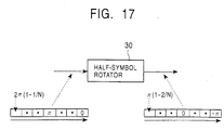
- the output data is supplied to the half-symbol rotator 30, which then temporarily stores, as illustrated in Fig. 17, the data and performs half-symbol rotation on the data. Accordingly, the frequency domain ranging from 0 to ⁇ of the output data of the output buffer memory 8 is converted to a range from - ⁇ to ⁇ .
- a half-symbol rotator 31 is provided, as shown in Fig. 18, prior to the input buffer memory 7.
- the input data having a frequency domain from - ⁇ to ⁇ is first rotated, as illustrated in Fig. 19, by an amount equal to a half symbol by the half-symbol rotator 31, and is then converted to a range from 0 to 2 ⁇ .
- the resulting data having the converted frequency domain is supplied to the IFFT calculating apparatus 50.
- the frequency domain of the output data of the FFT calculating apparatus 40 or the frequency domain of the input data of the IFFT calculating apparatus 50 is converted.
- embodiments of the present invention can convert the frequency domain for use in a FFT calculating apparatus or an IFFT calculating apparatus without needing to use an external circuit, thereby decreasing the scale of the circuitry.
- a calculating apparatus having first storage means for storing data to be input from an external source.
- Calculation means performs butterfly calculation.
- Second storage means stores data used for the calculation of the calculation means.
- Third storage means stores the data calculated by the calculation means and to be output to an external source.
- Setting means sets the order of write addresses or read addresses of the data to be stored in the first storage means or the third storage means.
- the first storage means or the third storage means writes or reads data in accordance with the order of addresses set by the setting means.
- the data whose upper half symbol and lower half symbol are transposed may be input or output.
- a calculating method for use in the foregoing calculating apparatus having a setting step of setting the order of write addresses or read addresses of the data to be stored in the first storage means or the third storage means.
- the first storage means or the third storage means writes or reads data in accordance with the order of addresses set by the setting step.
- the data whose upper half symbol and lower half symbol are transposed may be input or output.
- Fig. 1 is a block diagram illustrating the configuration of a calculating apparatus according to an embodiment of the present invention.
- a calculating apparatus 1 performs FFT calculation or IFFT calculation on input data and then outputs the calculated data.
- An input buffer memory 2 temporarily stores the input data and then outputs it to a memory 4 (may be to a butterfly calculator 3 if necessary).
- An output buffer 6 temporarily stores the final data of the calculating apparatus 1 and outputs it to an external source.
- the input buffer memory 2 or the output buffer memory 6 is provided with an address generating circuit 20 (which is described later in greater detail with reference to Fig. 4).
- the address generating circuit 20 arranges the write addresses or the read addresses of data in either buffer memory in a predetermined order.
- the address generating circuit 20 may be provided only for the output buffer memory 6 if the calculating apparatus 1 performs only FFT calculation. Conversely, the address generating circuit 20 may be provided only for the input buffer memory 2 if the calculating apparatus 1 performs only IFFT calculation.
- the calculation performed in the calculating apparatus 1 of this embodiment is basically similar to the FFT calculation made by the known FFT calculating apparatus 40 shown in Fig. 16 or the IFFT calculation made by the known IFFT calculating apparatus 50 shown in Fig. 18.
- the calculation of the calculating apparatus 1 differs from that of the above conventional apparatus 40 or 50 only in the operation of the input buffer memory 2 or the output buffer memory 6.
- a discussion is given below of the configuration and the operation of the input buffer memory 2 or the output buffer memory 6.
- both the input buffer memory 2 and the output buffer memory 6 have write addresses and read addresses, both of which range from 0 to (N-1), in order to store the data at the N points.
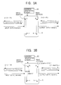
- FIG. 2A An embodiment of the input buffer memory 2 is shown in Figs. 2A and 2B.
- the address generating circuit 20 sets the order of writing data items into the input buffer memory 2 in such a manner that the data items are sequentially written into the write addresses from 0 to (N-1).
- the data items at the N points having an angular frequency ranging from 0 to 2 ⁇ (1 - 1/N) are sequentially written into the write addresses from 0 to (N-1).
- the written data items are sequentially read from the read addresses from 0 to (N-1). Namely, the data having a frequency domain from 0 to 2 ⁇ is input into the input buffer memory 2 and the data having a frequency domain from 0 to 2 ⁇ is output therefrom.
- the address generating circuit 20 sets the order of writing data items into the input buffer memory 2 in such a manner that the data items are sequentially written into the write addresses from (sttadr) to (N-1) and from 0 to (sttadr - 1).
- the write address (sttadr) is determined by the frequency domain of the input data.
- the data items at the N points having an angular frequency from (-2 (1- sttadr/N) ⁇ ) to (2 (sttadr - 1)/N) ⁇ ) are sequentially written into the predetermined write addresses from (sttadr) to (N-1) and then returned to the write address 0 and further to the write address (sttadr - 1).
- the write addresses from 0 to (N-1) that the data items having an angular frequency ranging from 0 to (2 ⁇ (1 - 1/N)) are sequentially stored.
- the written data items are sequentially read from the read addresses from 0 to N-1. Namely, the data having a frequency domain from - ⁇ to ⁇ is input into the input buffer memory 2 and the data having a frequency domain from 0 to 2 ⁇ is output therefrom.
- the order of write addresses is set to convert the frequency domain of the input data.
- the order of the read addresses may be set.
- FIG. 3A An embodiment of the output buffer memory 6 is shown in Figs. 3A and 3B.
- the output buffer memory 6 illustrated in Fig. 3A is similar to the input buffer memory 2 shown in Fig. 2A, and an explanation thereof is thus appropriately omitted.
- the address generating circuit 20 sets the order of writing data items into the output buffer memory 6 in such a manner that the data items are sequentially written into the write addresses from (sttadr) to (N-1) and from 0 to (sttadr - 1).
- the data items at the N points having an angular frequency from 0 to (2 ⁇ (1 - 1/N)), which are input according to the above order of write addresses, are sequentially written, as illustrated in Fig. 3B, starting from the write address (sttadr) to the address (N-1), and then returned to the address 0 and further written to the address (sttadr - 1).
- the order of the write addresses is set to convert the frequency domain of the output data.
- the order of read addresses may be set.
- an n-bit counter 10 loads the value and then starts counting in synchronization with the data input into either of the input buffer memory 2 or the output buffer memory 6.
- the counter 10 then divides the count level into the most significant bit (MSB) and the remaining (n-1) bits and outputs them.
- the MSB of the count level is supplied to a NOT circuit 11 and a selector (SEL) 12.
- the NOT circuit 11 inverts the MSB and then supplies it to the selector 12.
- the selector 12 outputs the not-inverted MSB directly supplied from the counter 10 when a selection signal transmitted from an exterior source indicates 0. In contrast, the selector 12 outputs the inverted MSB when a selection signal represents 1.
- output from the address generating circuit 20 is a total of n bits of the MSB (one bit) output from the selector 12 and the remaining (n-1) bits output from the counter 10.
- the above-described operation is sequentially performed to set the order of write addresses in each buffer memory.
- the counter 10 is required to have a number of at least n bits. Accordingly, if the least significant bit (LSB) is set to 0 bit, the MSB of the count level is the (n-1)th bit.
- the same address generating circuit 20 may be for common use of the input buffer memory 2 and the output buffer memory 6.
- the foregoing embodiments of the input buffer memory 2 and the output buffer memory 6 and the address generating circuit 20 are further described by using specific numeric values.
- the input buffer memory 2 and the output buffer memory 6 shown in Figs. 5 and 6 are similarly configured to those illustrated in Figs. 2 and 3, respectively, and an explanation thereof is thus appropriately omitted.
- Fig. 6B illustrates the operation of the output buffer memory 6 in which the input data having a frequency domain from 0 to ⁇ is converted to a range from - ⁇ to ⁇ .
- the number of addresses N is set to be 8
- the address generating circuit 20 sets the order of writing data items into the output buffer memory 6 in such a manner that the data items are sequentially written into the addresses from 4 to 7 and from 0 to 3 (which is described in greater detail later with reference to Fig. 7).
- input data having an angular frequency from 0 to (7 ⁇ /4) on eight points are written, starting from the write address 4 to the write address 7, and then returned to the write address 0 and further to the write address 3.
- the data items having an angular frequency of ⁇ , 5 ⁇ /4, 6 ⁇ /4, 7 ⁇ /4, 0, ⁇ /4, 2 ⁇ /4, and 3 ⁇ /4 are sequentially stored in the output buffer memory 6. Then, the written data items are sequentially read from the read addresses from 0 to 7. According to the foregoing operation, the data having a frequency domain from 0 to 2 ⁇ is input into the output buffer memory 6, and the data having a frequency domain from - ⁇ to ⁇ is output therefrom.
- the write address (sttadr) is set to be (N/2), as shown in Fig. 5B.
- data items are sequentially written into the write addresses from (N/2) to (N-1) and from 0 to (N/2 - 1) in the input buffer memory 2. Then, the data items are read from the addresses from 0 to (N-1).
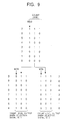
- the address generating circuit 20 illustrated in Fig. 7 is basically configured similarly to the counterpart shown in Fig. 4. However, the address generating circuit 20 shown in Fig. 7 uses a 3-bit counter 10. In response to an input of a load value (000), the counter 10 loads the value (000) and starts counting in synchronization with the data input into the output buffer memory 6. The counter 10 sequentially counts from 0 to 7, as illustrated in Fig. 9. During each counting operation, the counter 10 divides the count level into the MSB and the remaining bits and outputs them. The MSB is supplied to a selector 12 and a NOT circuit 11. The NOT circuit 11 inverts the MSB and supplies it to the selector 12.
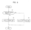
- Fig. 8 is a flow chart illustrating the operation of the selector 12.
- the selector 12 determines whether a control signal supplied from an exterior source is 1. If the answer of step S1 is yes, the process proceeds to step S2 in which the selector 12 outputs the MSB inverted by the NOT circuit 11. If the selector 12 finds in step S1 that the supplied control signal is not 1 (i.e., is 0), the process proceeds to step S3 in which the selector 12 outputs the not-inverted MSB directly supplied from the counter 10.
- the MSB (one bit) output from the selector 12 and the remaining two bits output from the counter 10 are output from the address generating circuit 20 as a total of a 3-bit address.
- the count levels are sequentially output from 4 to 7 and from 0 to 3 (decimal), as indicated by the lower left portion of Fig. 9.
- the selection signal 0 is supplied to the selector 12
- the count levels are sequentially output from 0 to 7, as represented by the lower right portion of Fig. 9.
- the data is written into the output buffer memory 6.
- the calculating apparatus and the calculating method of the present invention offers the following advantages.
- the order of writing data items or the order of reading data items into the input buffer memory or the output buffer memory can be set.
Landscapes
- Physics & Mathematics (AREA)
- Mathematical Physics (AREA)
- Engineering & Computer Science (AREA)
- General Physics & Mathematics (AREA)
- Computational Mathematics (AREA)
- Mathematical Analysis (AREA)
- Mathematical Optimization (AREA)
- Pure & Applied Mathematics (AREA)
- Data Mining & Analysis (AREA)
- Theoretical Computer Science (AREA)
- Discrete Mathematics (AREA)
- Algebra (AREA)
- Databases & Information Systems (AREA)
- Software Systems (AREA)
- General Engineering & Computer Science (AREA)
- Complex Calculations (AREA)
Applications Claiming Priority (3)
| Application Number | Priority Date | Filing Date | Title |
|---|---|---|---|
| JP13338097A JP3797400B2 (ja) | 1997-05-23 | 1997-05-23 | 演算装置および方法 |
| JP133380/97 | 1997-05-23 | ||
| JP13338097 | 1997-05-23 |
Publications (2)
| Publication Number | Publication Date |
|---|---|
| EP0880101A2 true EP0880101A2 (fr) | 1998-11-25 |
| EP0880101A3 EP0880101A3 (fr) | 2000-02-02 |
Family
ID=15103387
Family Applications (1)
| Application Number | Title | Priority Date | Filing Date |
|---|---|---|---|
| EP98304057A Ceased EP0880101A3 (fr) | 1997-05-23 | 1998-05-21 | Dispositif et méthode de calcul d'une transformation rapide de Fourier |
Country Status (3)
| Country | Link |
|---|---|
| US (1) | US6263356B1 (fr) |
| EP (1) | EP0880101A3 (fr) |
| JP (1) | JP3797400B2 (fr) |
Cited By (3)
| Publication number | Priority date | Publication date | Assignee | Title |
|---|---|---|---|---|
| WO2003041010A3 (fr) * | 2001-11-06 | 2003-12-18 | Infineon Technologies Ag | Architecture permettant des realiser des tranformees rapides de fourier directes et inverses |
| WO2007068438A3 (fr) * | 2005-12-14 | 2008-06-05 | Ericsson Telefon Ab L M | Transformation de fourier rapide circulaire |
| EP2407891A4 (fr) * | 2009-03-12 | 2015-01-21 | Zte Corp | Procédé et appareil de traitement pour mettre en uvre une ifft à l'aide d'une fft |
Families Citing this family (10)
| Publication number | Priority date | Publication date | Assignee | Title |
|---|---|---|---|---|
| US7062523B1 (en) * | 2000-08-01 | 2006-06-13 | Analog Devices, Inc. | Method for efficiently computing a fast fourier transform |
| US20050203578A1 (en) * | 2001-08-15 | 2005-09-15 | Weiner Michael L. | Process and apparatus for treating biological organisms |
| KR20040032683A (ko) * | 2002-10-10 | 2004-04-17 | 엘지전자 주식회사 | 무선 랜 시스템의 고속 푸리에 변환 장치 |
| TW594502B (en) * | 2003-01-30 | 2004-06-21 | Ind Tech Res Inst | Length-scalable fast Fourier transformation digital signal processing architecture |
| US7296045B2 (en) * | 2004-06-10 | 2007-11-13 | Hasan Sehitoglu | Matrix-valued methods and apparatus for signal processing |
| US20060075010A1 (en) * | 2004-10-05 | 2006-04-06 | Wadleigh Kevin R | Fast fourier transform method and apparatus |
| US8612504B2 (en) | 2006-04-04 | 2013-12-17 | Qualcomm Incorporated | IFFT processing in wireless communications |
| US8543629B2 (en) | 2006-04-04 | 2013-09-24 | Qualcomm Incorporated | IFFT processing in wireless communications |
| US7675847B2 (en) | 2007-07-10 | 2010-03-09 | Wipro Limited | Hardware implementation of a programmable FFT based on a half length FFT core |
| WO2025095327A1 (fr) * | 2023-11-01 | 2025-05-08 | 삼성전자주식회사 | Dispositif électronique et procédé pour une transformée de fourier rapide |
Citations (2)
| Publication number | Priority date | Publication date | Assignee | Title |
|---|---|---|---|---|
| US3731284A (en) * | 1971-12-27 | 1973-05-01 | Bell Telephone Labor Inc | Method and apparatus for reordering data |
| US3943347A (en) * | 1974-11-27 | 1976-03-09 | Rca Corporation | Data processor reorder random access memory |
Family Cites Families (6)
| Publication number | Priority date | Publication date | Assignee | Title |
|---|---|---|---|---|
| US3673399A (en) | 1970-05-28 | 1972-06-27 | Ibm | Fft processor with unique addressing |
| US4138730A (en) * | 1977-11-07 | 1979-02-06 | Communications Satellite Corporation | High speed FFT processor |
| JPH0746217A (ja) * | 1993-07-26 | 1995-02-14 | Sony Corp | ディジタル復調装置 |
| US5675572A (en) * | 1993-07-28 | 1997-10-07 | Sony Corporation | Orthogonal frequency division multiplex modulation apparatus and orthogonal frequency division multiplex demodulation apparatus |
| US5606575A (en) | 1993-10-29 | 1997-02-25 | Airnet Communications Corporation | FFT-based channelizer and combiner employing residue-adder-implemented phase advance |
| US5732113A (en) * | 1996-06-20 | 1998-03-24 | Stanford University | Timing and frequency synchronization of OFDM signals |
-
1997
- 1997-05-23 JP JP13338097A patent/JP3797400B2/ja not_active Expired - Fee Related
-
1998
- 1998-05-20 US US09/081,921 patent/US6263356B1/en not_active Expired - Fee Related
- 1998-05-21 EP EP98304057A patent/EP0880101A3/fr not_active Ceased
Patent Citations (2)
| Publication number | Priority date | Publication date | Assignee | Title |
|---|---|---|---|---|
| US3731284A (en) * | 1971-12-27 | 1973-05-01 | Bell Telephone Labor Inc | Method and apparatus for reordering data |
| US3943347A (en) * | 1974-11-27 | 1976-03-09 | Rca Corporation | Data processor reorder random access memory |
Non-Patent Citations (3)
| Title |
|---|
| BIDET E ET AL: "A fast single-chip implementation of 8192 complex point FFT", IEEE JOURNAL OF SOLID-STATE CIRCUITS, vol. 30, no. 3, March 1995 (1995-03-01), pages 300 - 305, XP000502815 * |
| CHOINSKI T C ET AL: "Generation of digit reversed address sequences for fast Fourier transforms", IEEE TRANSACTIONS ON COMPUTERS, vol. 40, no. 6, June 1991 (1991-06-01), pages 780 - 784, XP000258574 * |
| DIEFFENDORFER J W: "Pipeline fast Fourier transform processor", IBM TECHNICAL DISCLOSURE BULLETIN, vol. 16, no. 2, July 1973 (1973-07-01), pages 530 - 533 * |
Cited By (6)
| Publication number | Priority date | Publication date | Assignee | Title |
|---|---|---|---|---|
| WO2003041010A3 (fr) * | 2001-11-06 | 2003-12-18 | Infineon Technologies Ag | Architecture permettant des realiser des tranformees rapides de fourier directes et inverses |
| WO2007068438A3 (fr) * | 2005-12-14 | 2008-06-05 | Ericsson Telefon Ab L M | Transformation de fourier rapide circulaire |
| US7685220B2 (en) | 2005-12-14 | 2010-03-23 | Telefonaktiebolaget L M Ericsson (Publ) | Circular fast fourier transform |
| CN101331479B (zh) * | 2005-12-14 | 2012-01-11 | Lm爱立信电话有限公司 | 快速傅里叶变换级电路、处理器和方法及正交频分复用接收器 |
| KR101229648B1 (ko) * | 2005-12-14 | 2013-02-04 | 텔레폰악티에볼라겟엘엠에릭슨(펍) | 순환 급속 푸리에 변환 |
| EP2407891A4 (fr) * | 2009-03-12 | 2015-01-21 | Zte Corp | Procédé et appareil de traitement pour mettre en uvre une ifft à l'aide d'une fft |
Also Published As
| Publication number | Publication date |
|---|---|
| JP3797400B2 (ja) | 2006-07-19 |
| US6263356B1 (en) | 2001-07-17 |
| JPH10327123A (ja) | 1998-12-08 |
| EP0880101A3 (fr) | 2000-02-02 |
Similar Documents
| Publication | Publication Date | Title |
|---|---|---|
| US6263356B1 (en) | Fast fourier transform calculating apparatus and fast fourier transform calculating method | |
| JP4022546B2 (ja) | 高速フーリエ変換を用いた混合−基数方式の変調装置 | |
| US6115728A (en) | Fast fourier transforming apparatus and method, variable bit reverse circuit, inverse fast fourier transforming apparatus and method, and OFDM receiver and transmitter | |
| US5954787A (en) | Method of generating sine/cosine function and apparatus using the same for use in digital signal processor | |
| JPH0631990B2 (ja) | 波形の補間装置 | |
| JPS60140463A (ja) | 集積化データ処理装置 | |
| US20050177608A1 (en) | Fast Fourier transform processor and method using half-sized memory | |
| US9900201B2 (en) | Time de-interleaving circuit and method thereof | |
| JP3065979B2 (ja) | 高速フーリエ変換装置および方法、可変ビットリバース回路、逆高速フーリエ変換装置および方法、並びにofdm受信および送信装置 | |
| US6320431B1 (en) | Apparatus and method of generating numerically controlled oscillator signals | |
| JP2001056806A (ja) | 高速フーリエ変換装置 | |
| US6127860A (en) | Linear expansion based sine generator | |
| US6501470B1 (en) | Look-up table device and image generation device | |
| US7219116B2 (en) | Data processing apparatus | |
| US7565595B2 (en) | Convolutional interleaving and de-interleaving circuit and method thereof | |
| JPH08191217A (ja) | 正弦波発生回路 | |
| JP3639424B2 (ja) | アドレス発生回路 | |
| KR100203237B1 (ko) | 디지탈 정현파 출력 방법 및 그 장치 | |
| JP2000112715A (ja) | 正弦・余弦演算回路 | |
| US6785343B1 (en) | Rectangular-to-polar conversion angle quantizer | |
| KR100328840B1 (ko) | 사인/코사인 연산장치 | |
| JPS6043742A (ja) | 可変長デ−タ読出し回路 | |
| JPH0750693A (ja) | π/4シフトQPSK変調器、並びにそれを用いた通信装置 | |
| JPH05266059A (ja) | アドレス発生回路 | |
| JP3455828B2 (ja) | ビットシフト回路 |
Legal Events
| Date | Code | Title | Description |
|---|---|---|---|
| PUAI | Public reference made under article 153(3) epc to a published international application that has entered the european phase |
Free format text: ORIGINAL CODE: 0009012 |
|
| AK | Designated contracting states |
Kind code of ref document: A2 Designated state(s): AT DE ES FR GB NL SE |
|
| AX | Request for extension of the european patent |
Free format text: AL;LT;LV;MK;RO;SI |
|
| PUAL | Search report despatched |
Free format text: ORIGINAL CODE: 0009013 |
|
| AK | Designated contracting states |
Kind code of ref document: A3 Designated state(s): AT BE CH CY DE DK ES FI FR GB GR IE IT LI LU MC NL PT SE |
|
| AX | Request for extension of the european patent |
Free format text: AL;LT;LV;MK;RO;SI |
|
| 17P | Request for examination filed |
Effective date: 20000704 |
|
| AKX | Designation fees paid |
Free format text: AT DE ES FR GB NL SE |
|
| 17Q | First examination report despatched |
Effective date: 20071123 |
|
| STAA | Information on the status of an ep patent application or granted ep patent |
Free format text: STATUS: THE APPLICATION HAS BEEN REFUSED |
|
| 18R | Application refused |
Effective date: 20100913 |