EP0880167A2 - Kondensator mit einem verbesserten Dielektrikum auf Basis von TaOx - Google Patents
Kondensator mit einem verbesserten Dielektrikum auf Basis von TaOx Download PDFInfo
- Publication number
- EP0880167A2 EP0880167A2 EP98303706A EP98303706A EP0880167A2 EP 0880167 A2 EP0880167 A2 EP 0880167A2 EP 98303706 A EP98303706 A EP 98303706A EP 98303706 A EP98303706 A EP 98303706A EP 0880167 A2 EP0880167 A2 EP 0880167A2
- Authority
- EP
- European Patent Office
- Prior art keywords
- capacitors
- dielectric
- capacitor
- film
- dielectric layer
- Prior art date
- Legal status (The legal status is an assumption and is not a legal conclusion. Google has not performed a legal analysis and makes no representation as to the accuracy of the status listed.)
- Granted
Links
Images


Classifications
-
- H—ELECTRICITY
- H10—SEMICONDUCTOR DEVICES; ELECTRIC SOLID-STATE DEVICES NOT OTHERWISE PROVIDED FOR
- H10D—INORGANIC ELECTRIC SEMICONDUCTOR DEVICES
- H10D1/00—Resistors, capacitors or inductors
- H10D1/60—Capacitors
- H10D1/68—Capacitors having no potential barriers
-
- H—ELECTRICITY
- H01—ELECTRIC ELEMENTS
- H01G—CAPACITORS; CAPACITORS, RECTIFIERS, DETECTORS, SWITCHING DEVICES, LIGHT-SENSITIVE OR TEMPERATURE-SENSITIVE DEVICES OF THE ELECTROLYTIC TYPE
- H01G4/00—Fixed capacitors; Processes of their manufacture
- H01G4/002—Details
- H01G4/018—Dielectrics
- H01G4/06—Solid dielectrics
- H01G4/08—Inorganic dielectrics
-
- H—ELECTRICITY
- H10—SEMICONDUCTOR DEVICES; ELECTRIC SOLID-STATE DEVICES NOT OTHERWISE PROVIDED FOR
- H10P—GENERIC PROCESSES OR APPARATUS FOR THE MANUFACTURE OR TREATMENT OF DEVICES COVERED BY CLASS H10
- H10P14/00—Formation of materials, e.g. in the shape of layers or pillars
- H10P14/60—Formation of materials, e.g. in the shape of layers or pillars of insulating materials
- H10P14/69—Inorganic materials
- H10P14/692—Inorganic materials composed of oxides, glassy oxides or oxide-based glasses
- H10P14/6938—Inorganic materials composed of oxides, glassy oxides or oxide-based glasses the material containing at least one metal element, e.g. metal oxides, metal oxynitrides or metal oxycarbides
- H10P14/6939—Inorganic materials composed of oxides, glassy oxides or oxide-based glasses the material containing at least one metal element, e.g. metal oxides, metal oxynitrides or metal oxycarbides characterised by the metal
- H10P14/69391—Inorganic materials composed of oxides, glassy oxides or oxide-based glasses the material containing at least one metal element, e.g. metal oxides, metal oxynitrides or metal oxycarbides characterised by the metal the material containing aluminium, e.g. Al2O3
-
- H—ELECTRICITY
- H10—SEMICONDUCTOR DEVICES; ELECTRIC SOLID-STATE DEVICES NOT OTHERWISE PROVIDED FOR
- H10P—GENERIC PROCESSES OR APPARATUS FOR THE MANUFACTURE OR TREATMENT OF DEVICES COVERED BY CLASS H10
- H10P14/00—Formation of materials, e.g. in the shape of layers or pillars
- H10P14/60—Formation of materials, e.g. in the shape of layers or pillars of insulating materials
- H10P14/69—Inorganic materials
- H10P14/692—Inorganic materials composed of oxides, glassy oxides or oxide-based glasses
- H10P14/6938—Inorganic materials composed of oxides, glassy oxides or oxide-based glasses the material containing at least one metal element, e.g. metal oxides, metal oxynitrides or metal oxycarbides
- H10P14/6939—Inorganic materials composed of oxides, glassy oxides or oxide-based glasses the material containing at least one metal element, e.g. metal oxides, metal oxynitrides or metal oxycarbides characterised by the metal
- H10P14/69393—Inorganic materials composed of oxides, glassy oxides or oxide-based glasses the material containing at least one metal element, e.g. metal oxides, metal oxynitrides or metal oxycarbides characterised by the metal the material containing tantalum, e.g. Ta2O5
-
- H—ELECTRICITY
- H10—SEMICONDUCTOR DEVICES; ELECTRIC SOLID-STATE DEVICES NOT OTHERWISE PROVIDED FOR
- H10P—GENERIC PROCESSES OR APPARATUS FOR THE MANUFACTURE OR TREATMENT OF DEVICES COVERED BY CLASS H10
- H10P14/00—Formation of materials, e.g. in the shape of layers or pillars
- H10P14/60—Formation of materials, e.g. in the shape of layers or pillars of insulating materials
- H10P14/69—Inorganic materials
- H10P14/692—Inorganic materials composed of oxides, glassy oxides or oxide-based glasses
- H10P14/6938—Inorganic materials composed of oxides, glassy oxides or oxide-based glasses the material containing at least one metal element, e.g. metal oxides, metal oxynitrides or metal oxycarbides
- H10P14/6939—Inorganic materials composed of oxides, glassy oxides or oxide-based glasses the material containing at least one metal element, e.g. metal oxides, metal oxynitrides or metal oxycarbides characterised by the metal
- H10P14/69397—Inorganic materials composed of oxides, glassy oxides or oxide-based glasses the material containing at least one metal element, e.g. metal oxides, metal oxynitrides or metal oxycarbides characterised by the metal the material containing two or more metal elements
Definitions
- This application pertains to TaO x -based dielectrics, typically to such dielectrics for integrated circuits (ICs).
- TaO x , x ⁇ 2.5 The relatively high dielectric constant and breakdown field strength of tantalum oxide (herein generally TaO x , x ⁇ 2.5) make thin film TaO x potentially useful for integrated circuit applications.
- TaO x -based dielectric material before TaO x -based dielectric material can be used in production devices, some properties of the material have to be improved. Among these are leakage current which, at least for some IC applications, desirably is reduced over typical prior art values, and breakdown voltage, which desirably is raised.
- post-deposition annealing Two approaches have dominated the efforts to improve the dielectric properties, namely, post-deposition annealing, and incorporation of one or more further metal oxides such as Al 2 O 2 , TiO 2 , WO 3 , SiO 2 or ZrO 2 into the film.
- the former requires relatively high temperatures, and may lead to crystallization of the TaO x , a deleterious change.
- post-deposition annealing to date has yielded only marginal improvements in leakage current and breakdown voltage.
- US patent 4,038,167 discloses formation of a thin film capacitor by a method that comprises RF sputtering a film of Ta oxide in an O 2 -N 2 inert gas atmosphere.
- TaO x -based dielectric film that can have relatively low leakage current and relatively high breakdown voltage. This application discloses such a film, and a method of making the film.
- CV br /A corresponds to the maximum charge that can be stored on the capacitor.
- V br is determined by passing a DC current (e.g., 10 nA) for maximally 10s through the capacitor and measuring the voltage developed across the capacitor.
- the maximum voltage developed (herein designated V * ) is used as an estimate of V br .
- V * the figure of merit
- CV * /A is independent of the thickness of the dielectric layer as long as ⁇ and E br are independent of thickness.
- the value of V * typically depends on the polarity of the measurement current.
- the polarity is selected such that electrons are injected into the dielectric film from a Hg probe electrode.
- Dielectric films were deposited by a known method, off-axis reactive co-sputtering, in a commercially available apparatus. However, it is expected that other appropriate deposition techniques (e.g., on-axis reactive sputtering with a composite target, chemical vapor deposition, etc.) will yield comparable results.
- the Ta gun was typically run at 100W, while the power to the Al gun was varied to provide an appropriate Al/Ta ratio at the substrate midpoint.
- Typical deposition parameters are listed in Table I. Exemplarily the depositions were performed at a total pressure of 30 mT (4 Pa), using flow rates of 40, 10 and 2.5 sccm for Ar, O 2 and N 2 , respectively.
- the substrates were conventional Si wafers with 550 nm of thermal oxide, coated with 45 nm of Ti and 60 nm of TiN.
- the substrate temperature typically did not rise above 50°C during a typical 20 minute deposition run.
- Dielectric films according to the invention have composition Ta 1-y Al y O x N z , possibly with a trace amount of Ar as an unintended impurity.
- Film thickness and cation composition as a function of position on the wafer were determined by conventional techniques, including Rutherford Backscattering.
- the cation composition parameter y typically is in the range 0.05-0.5, with values below the lower limit typically not giving significant improvement in the dielectric properties, and values above the upper limit significantly reducing the figure of merit, as the lower dielectric constant of AlO x begins to dominate without compensating increase in E br .
- the anion composition parameter x typically is less than about 2.5 (typically about 2.35), and the parameter z typically is in the range 0.01-0.1, with x+z typically being about 2.4, to within about 10%.
- Table II shows exemplary data for comparison films (Ta-oxide film prepared using commercially available on-axis sputtering equipment, Ta-oxide film prepared using off-axis sputtering equipment, Ta-Al-oxide film, and Ta-O-N film), as well as for Ta-Al-O-N film according to the invention.
- the unexpected improvement in the dielectric properties of the film according to the invention over the comparison films is evident from the data of Table II.
- the figure of merit (Y 3.0 ) of a multi-capacitor sample of capacitors with dielectric according to the invention typically substantially exceeds that of a comparison sample of capacitors with the prior art dielectric tantalum oxide.
- Y 3.0 of the former will be at least 75%, preferably more than 80%.
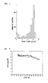
- FIG. 1 shows the data corresponding to the first line of Table II. Clearly, most of the capacitors had CV * /A ⁇ 4 ⁇ coulomb/cm 2 .
- the Ta-O capacitors were prepared using a commercial apparatus (CVC, Inc., of Rochester, NY) using on-axis sputtering, a standard process for depositing thin film TaO x capacitors, and the results demonstrate the typical quality obtained.
- the data of FIG. 1 is presented as a benchmark against which the dielectric layers according to the invention can be compared.
- FIG. 2 shows the data corresponding to line 2 of Table II, namely a TaO x film grown by off-axis sputtering in our deposition apparatus.
- the film has a slightly lower value of Y 3.0 and a slightly higher value of M 3.0 than the benchmark film of FIG. 1.
- the lower value of Y 3.0 can be attributed at least in part to an edge effect and thus is not inherent. Indeed, we conclude that the off-axis film of FIG. 2 is of quality comparable to that of the benchmark film.
- FIG. 3 shows measurement results on Ta 1-y Al y O x films produced by off-axis co-sputtering of Ta and Al in Ar and 02. It has been reported (e.g., K. Nomura et al., op. cit.) that the addition of Al to TaO x results in improved breakdown voltage, and thus in improved CV * /A. Although our results show some capacitors with improved figure of merit, up to a value of 8.0 ⁇ coulomb/cm 2 , the yield of good capacitors (Y 3.0 ) of the Al-doped capacitors is much less than for the benchmark film. Inspection of the data as a function of Al content indicates that this result is consistent over the range 0.05 ⁇ y ⁇ 0.5 in Ta 1-y Al y O x .
- FIG. 4 shows measurement results on TaO x N z dielectric film, produced by off-axis sputtering as described above, i.e., by adding 5 vol. % N 2 to the Ar/O 2 mix.
- doping of TaO x with nitrogen does not significantly improve the dielectric properties of the films, as compared to the benchmark film.
- FIG. 6 shows CV * /A as a function of the Al-content for dielectric films according to the invention.
- the data reveals the decrease in the figure of merit for y > 0.4.
- Al may not be the only cation substituent that can provide improved dielectric properties, to date we have not found any other beneficial cation substituent. Specifically, additions of 5-50 at % of Si, Ge, Sn or Ti, each with and without N 2 in the sputtering atmosphere, either had not effect or decreased Y 3.0 .
- FIG. 8 schematically depicts a capacitor 80 according to the invention on a substrate 81 (exemplarily a Si chip).
- the capacitor comprises electrodes 82 and 84, with a dielectric layer 83 according to the invention therebetween.
- the capacitor will be part of an integrated circuit. Such a circuit can be conventional and does not require detailed description.
- dielectric layer 83 is not necessarily of constant composition throughout the layer thickness. Indeed, in some embodiments capacitors according to the invention will have a compound dielectric layer, exemplarily comprising alternating layers of material according to the invention and another dielectric material (e.g., Al 2 O 3 ), or comprising a layer of material according to the invention, either sandwiched between two layers of another dielectric material (e.g., Al 2 O 3 ), or sandwiched between one layer of another dielectric material and one of the conductor layers.
- a compound dielectric layer exemplarily comprising alternating layers of material according to the invention and another dielectric material (e.g., Al 2 O 3 ), or comprising a layer of material according to the invention, either sandwiched between two layers of another dielectric material (e.g., Al 2 O 3 ), or sandwiched between one layer of another dielectric material and one of the conductor layers.
- Example 1 Material according to the invention was produced by off-axis co-sputtering deposition as follows.
- a conventional Si substrate with 60 nm TiN was provided and mounted onto the aluminum sample holder of the sputtering apparatus such that the sample was positioned 3.0 cm from the Ta-metal magnetron sputter gun target, and 8.0 cm from the Al-metal magnetron sputter gun target.
- the two sputter guns were positioned with targets facing each other. The sample was positioned such that its plane is parallel to the line connecting the centers of the two targets, and displaced 3.5 cm from that line.
- the system was evacuated to less than 5 x 10 -6 Torr, followed by establishing flows of 2.5 sccm N 2 , 10 sccm O 2 , and 40 sccm Ar.
- the high vacuum pump was throttled to obtain a total gas pressure of 30.0 mTorr.
- 10 W of rf power were applied to the substrate, and 100 W and 40 W of rf power were applied to the Ta gun and the Al gun, respectively.
- the matching circuits were tuned to respectively obtain minimum reflected power. Maintaining these conditions for 20 minutes resulted in deposition of a Ta-Al-oxygen-nitrogen film of thickness and composition that depends on position on the substrate.
- capacitance measurements were made substantially as described above. The measurements yielded figure of merit data substantially as shown in FIG. 5.
- Example 2 Material according to the invention was produced by on-axis sputter deposition as follows.
- a substrate was provided as in Example 1.
- a Ta 0.9 Al 0.1 composite 2 inch diameter sputtering target was mounted in the magnetron sputtering gun.
- the substrate was mounted onto the sample holder/heater with Ta clips such that the substrate faced the sputtering target and was spaced 9.0 cm therefrom.
- the substrate was heated to 250°C, and gas (1 sccm N 2 , 5 sccm O 2 , 5 sccm Ar) was introduced, with the high vacuum pump throttled to give 10 mTorr total gas pressure.
Landscapes
- Engineering & Computer Science (AREA)
- Power Engineering (AREA)
- Chemical & Material Sciences (AREA)
- Inorganic Chemistry (AREA)
- Manufacturing & Machinery (AREA)
- Microelectronics & Electronic Packaging (AREA)
- Semiconductor Integrated Circuits (AREA)
- Fixed Capacitors And Capacitor Manufacturing Machines (AREA)
- Formation Of Insulating Films (AREA)
- Physical Vapour Deposition (AREA)
Applications Claiming Priority (2)
| Application Number | Priority Date | Filing Date | Title |
|---|---|---|---|
| US862907 | 1997-05-23 | ||
| US08/862,907 US5977582A (en) | 1997-05-23 | 1997-05-23 | Capacitor comprising improved TaOx -based dielectric |
Publications (3)
| Publication Number | Publication Date |
|---|---|
| EP0880167A2 true EP0880167A2 (de) | 1998-11-25 |
| EP0880167A3 EP0880167A3 (de) | 1998-12-02 |
| EP0880167B1 EP0880167B1 (de) | 2000-09-06 |
Family
ID=25339709
Family Applications (1)
| Application Number | Title | Priority Date | Filing Date |
|---|---|---|---|
| EP98303706A Expired - Lifetime EP0880167B1 (de) | 1997-05-23 | 1998-05-12 | Kondensator mit einem verbesserten Dielektrikum auf Basis von TaOx |
Country Status (6)
| Country | Link |
|---|---|
| US (1) | US5977582A (de) |
| EP (1) | EP0880167B1 (de) |
| JP (1) | JP3464607B2 (de) |
| KR (1) | KR100505305B1 (de) |
| DE (1) | DE69800287T2 (de) |
| TW (1) | TW434785B (de) |
Families Citing this family (55)
| Publication number | Priority date | Publication date | Assignee | Title |
|---|---|---|---|---|
| US6060406A (en) * | 1998-05-28 | 2000-05-09 | Lucent Technologies Inc. | MOS transistors with improved gate dielectrics |
| JP2000003991A (ja) * | 1998-06-15 | 2000-01-07 | Mitsubishi Electric Corp | 半導体装置およびその製造方法 |
| KR100359860B1 (ko) * | 1998-12-31 | 2003-02-20 | 주식회사 하이닉스반도체 | 반도체 소자의 캐패시터 형성방법 |
| KR100331271B1 (ko) | 1999-07-01 | 2002-04-06 | 박종섭 | TaON박막을 갖는 커패시터 제조방법 |
| US6352944B1 (en) * | 1999-02-10 | 2002-03-05 | Micron Technology, Inc. | Method of depositing an aluminum nitride comprising layer over a semiconductor substrate |
| KR100335775B1 (ko) * | 1999-06-25 | 2002-05-09 | 박종섭 | 반도체 소자의 캐패시터 제조 방법 |
| GB2355113B (en) | 1999-06-25 | 2004-05-26 | Hyundai Electronics Ind | Method of manufacturing capacitor for semiconductor memory device |
| KR100328454B1 (ko) | 1999-06-29 | 2002-03-16 | 박종섭 | 반도체 소자의 캐패시터 제조 방법 |
| KR100331270B1 (ko) | 1999-07-01 | 2002-04-06 | 박종섭 | TaON박막을 갖는 커패시터 제조방법 |
| KR100305076B1 (ko) | 1999-07-01 | 2001-11-01 | 박종섭 | 커패시터의 전하저장전극 형성방법 |
| GB2358284B (en) | 1999-07-02 | 2004-07-14 | Hyundai Electronics Ind | Method of manufacturing capacitor for semiconductor memory device |
| KR100624903B1 (ko) * | 1999-12-22 | 2006-09-19 | 주식회사 하이닉스반도체 | 반도체 소자의 캐패시터 제조방법 |
| KR100705926B1 (ko) * | 1999-12-22 | 2007-04-11 | 주식회사 하이닉스반도체 | 반도체 소자의 캐패시터 제조방법 |
| KR100417855B1 (ko) * | 2001-04-30 | 2004-02-11 | 주식회사 하이닉스반도체 | 반도체소자의 캐패시터 및 그 제조방법 |
| US7469558B2 (en) | 2001-07-10 | 2008-12-30 | Springworks, Llc | As-deposited planar optical waveguides with low scattering loss and methods for their manufacture |
| US6677254B2 (en) | 2001-07-23 | 2004-01-13 | Applied Materials, Inc. | Processes for making a barrier between a dielectric and a conductor and products produced therefrom |
| US6946408B2 (en) * | 2001-10-24 | 2005-09-20 | Applied Materials, Inc. | Method and apparatus for depositing dielectric films |
| US7404877B2 (en) | 2001-11-09 | 2008-07-29 | Springworks, Llc | Low temperature zirconia based thermal barrier layer by PVD |
| KR100444603B1 (ko) * | 2001-12-22 | 2004-08-16 | 주식회사 하이닉스반도체 | 탄탈륨 펜타 옥사이드-알루미늄 옥사이드 유전체막 제조방법 및 이를 적용한 반도체 소자 |
| US7378356B2 (en) | 2002-03-16 | 2008-05-27 | Springworks, Llc | Biased pulse DC reactive sputtering of oxide films |
| US6884327B2 (en) | 2002-03-16 | 2005-04-26 | Tao Pan | Mode size converter for a planar waveguide |
| US6576482B1 (en) * | 2002-05-07 | 2003-06-10 | Texas Instruments Incorporated | One step deposition process for the top electrode and hardmask in a ferroelectric memory cell |
| KR100474592B1 (ko) * | 2002-06-28 | 2005-03-10 | 주식회사 하이닉스반도체 | 캐패시터 형성 방법 |
| US8021778B2 (en) | 2002-08-09 | 2011-09-20 | Infinite Power Solutions, Inc. | Electrochemical apparatus with barrier layer protected substrate |
| US8445130B2 (en) | 2002-08-09 | 2013-05-21 | Infinite Power Solutions, Inc. | Hybrid thin-film battery |
| US8431264B2 (en) | 2002-08-09 | 2013-04-30 | Infinite Power Solutions, Inc. | Hybrid thin-film battery |
| US7993773B2 (en) | 2002-08-09 | 2011-08-09 | Infinite Power Solutions, Inc. | Electrochemical apparatus with barrier layer protected substrate |
| US20070264564A1 (en) | 2006-03-16 | 2007-11-15 | Infinite Power Solutions, Inc. | Thin film battery on an integrated circuit or circuit board and method thereof |
| US8394522B2 (en) | 2002-08-09 | 2013-03-12 | Infinite Power Solutions, Inc. | Robust metal film encapsulation |
| US8236443B2 (en) | 2002-08-09 | 2012-08-07 | Infinite Power Solutions, Inc. | Metal film encapsulation |
| US8404376B2 (en) | 2002-08-09 | 2013-03-26 | Infinite Power Solutions, Inc. | Metal film encapsulation |
| AU2003261463A1 (en) | 2002-08-27 | 2004-03-19 | Symmorphix, Inc. | Optically coupling into highly uniform waveguides |
| US7205662B2 (en) | 2003-02-27 | 2007-04-17 | Symmorphix, Inc. | Dielectric barrier layer films |
| US7238628B2 (en) | 2003-05-23 | 2007-07-03 | Symmorphix, Inc. | Energy conversion and storage films and devices by physical vapor deposition of titanium and titanium oxides and sub-oxides |
| US8728285B2 (en) | 2003-05-23 | 2014-05-20 | Demaray, Llc | Transparent conductive oxides |
| KR101127370B1 (ko) | 2004-12-08 | 2012-03-29 | 인피니트 파워 솔루션스, 인크. | LiCoO2의 증착 |
| US7959769B2 (en) | 2004-12-08 | 2011-06-14 | Infinite Power Solutions, Inc. | Deposition of LiCoO2 |
| US7838133B2 (en) | 2005-09-02 | 2010-11-23 | Springworks, Llc | Deposition of perovskite and other compound ceramic films for dielectric applications |
| CN101523571A (zh) | 2006-09-29 | 2009-09-02 | 无穷动力解决方案股份有限公司 | 柔性基板上沉积的电池层的掩模和材料限制 |
| US8197781B2 (en) | 2006-11-07 | 2012-06-12 | Infinite Power Solutions, Inc. | Sputtering target of Li3PO4 and method for producing same |
| CN101903560B (zh) | 2007-12-21 | 2014-08-06 | 无穷动力解决方案股份有限公司 | 用于电解质膜的溅射靶的方法 |
| US8268488B2 (en) | 2007-12-21 | 2012-09-18 | Infinite Power Solutions, Inc. | Thin film electrolyte for thin film batteries |
| US8518581B2 (en) | 2008-01-11 | 2013-08-27 | Inifinite Power Solutions, Inc. | Thin film encapsulation for thin film batteries and other devices |
| WO2009124191A2 (en) | 2008-04-02 | 2009-10-08 | Infinite Power Solutions, Inc. | Passive over/under voltage control and protection for energy storage devices associated with energy harvesting |
| JP2012500610A (ja) | 2008-08-11 | 2012-01-05 | インフィニット パワー ソリューションズ, インコーポレイテッド | 電磁エネルギー獲得ための統合コレクタ表面を有するエネルギーデバイスおよびその方法 |
| CN102150185B (zh) | 2008-09-12 | 2014-05-28 | 无穷动力解决方案股份有限公司 | 具有经由电磁能进行数据通信的组成导电表面的能量装置及其方法 |
| WO2010042594A1 (en) | 2008-10-08 | 2010-04-15 | Infinite Power Solutions, Inc. | Environmentally-powered wireless sensor module |
| CN102576828B (zh) | 2009-09-01 | 2016-04-20 | 萨普拉斯特研究有限责任公司 | 具有集成薄膜电池的印刷电路板 |
| EP2577777B1 (de) | 2010-06-07 | 2016-12-28 | Sapurast Research LLC | Wiederaufladbare elektrochemische vorrichtung von hoher dichte |
| US8853819B2 (en) | 2011-01-07 | 2014-10-07 | Advanced Semiconductor Engineering, Inc. | Semiconductor structure with passive element network and manufacturing method thereof |
| US9368392B2 (en) | 2014-04-10 | 2016-06-14 | Taiwan Semiconductor Manufacturing Co., Ltd. | MIM capacitor structure |
| US9391016B2 (en) * | 2014-04-10 | 2016-07-12 | Taiwan Semiconductor Manufacturing Co., Ltd. | MIM capacitor structure |
| US9219110B2 (en) | 2014-04-10 | 2015-12-22 | Taiwan Semiconductor Manufacturing Co., Ltd. | MIM capacitor structure |
| US9425061B2 (en) | 2014-05-29 | 2016-08-23 | Taiwan Semiconductor Manufacturing Co., Ltd. | Buffer cap layer to improve MIM structure performance |
| JP6155420B2 (ja) * | 2014-08-08 | 2017-07-05 | 株式会社野田スクリーン | 薄膜キャパシタシートの製造方法 |
Family Cites Families (14)
| Publication number | Priority date | Publication date | Assignee | Title |
|---|---|---|---|---|
| GB1424980A (en) * | 1973-06-20 | 1976-02-11 | Siemens Ag | Thin-film electrical circuits |
| US4038167A (en) * | 1976-02-09 | 1977-07-26 | Corning Glass Works | Method of forming a thin film capacitor |
| US4200502A (en) * | 1979-03-12 | 1980-04-29 | Siemens Aktiengesellschaft | Method for producing an electrical thin layer circuit |
| JPS57113264A (en) * | 1980-12-29 | 1982-07-14 | Fujitsu Ltd | Manufacture of mis type capacitor |
| US4471405A (en) * | 1981-12-28 | 1984-09-11 | International Business Machines Corporation | Thin film capacitor with a dual bottom electrode structure |
| JPS6028259A (ja) * | 1983-07-26 | 1985-02-13 | Nec Corp | 半導体装置用キヤパシタの製造方法 |
| JPS61156865A (ja) * | 1984-12-28 | 1986-07-16 | Nec Corp | 半導体装置 |
| US4969032A (en) * | 1988-07-18 | 1990-11-06 | Motorola Inc. | Monolithic microwave integrated circuit having vertically stacked components |
| US5111355A (en) * | 1990-09-13 | 1992-05-05 | National Semiconductor Corp. | High value tantalum oxide capacitor |
| JPH0521744A (ja) * | 1991-07-10 | 1993-01-29 | Sony Corp | 半導体記憶装置のキヤパシタおよびその製造方法 |
| JPH0745467A (ja) * | 1993-07-26 | 1995-02-14 | Alps Electric Co Ltd | 誘電体およびこの誘電体を有するキャパシタ |
| US5479316A (en) * | 1993-08-24 | 1995-12-26 | Analog Devices, Inc. | Integrated circuit metal-oxide-metal capacitor and method of making same |
| EP0704880A3 (de) * | 1994-09-28 | 1998-09-30 | Matsushita Electric Industrial Co., Ltd. | Hochdruck-Entladungslampe, Herstellungsverfahren einer Entladungsröhre für Hochdruck-Entladungslampen und Herstellungsverfahren eines Hohlröhrenkörpers |
| JPH08148380A (ja) * | 1994-11-15 | 1996-06-07 | Kyocera Corp | Cr複合部品 |
-
1997
- 1997-05-23 US US08/862,907 patent/US5977582A/en not_active Expired - Lifetime
-
1998
- 1998-04-13 TW TW087105577A patent/TW434785B/zh not_active IP Right Cessation
- 1998-05-12 DE DE69800287T patent/DE69800287T2/de not_active Expired - Lifetime
- 1998-05-12 EP EP98303706A patent/EP0880167B1/de not_active Expired - Lifetime
- 1998-05-22 KR KR10-1998-0018520A patent/KR100505305B1/ko not_active Expired - Lifetime
- 1998-05-22 JP JP14098998A patent/JP3464607B2/ja not_active Expired - Lifetime
Also Published As
| Publication number | Publication date |
|---|---|
| TW434785B (en) | 2001-05-16 |
| US5977582A (en) | 1999-11-02 |
| EP0880167B1 (de) | 2000-09-06 |
| KR19980087299A (ko) | 1998-12-05 |
| DE69800287D1 (de) | 2000-10-12 |
| KR100505305B1 (ko) | 2005-10-26 |
| JPH10340999A (ja) | 1998-12-22 |
| DE69800287T2 (de) | 2001-01-25 |
| EP0880167A3 (de) | 1998-12-02 |
| JP3464607B2 (ja) | 2003-11-10 |
Similar Documents
| Publication | Publication Date | Title |
|---|---|---|
| EP0880167B1 (de) | Kondensator mit einem verbesserten Dielektrikum auf Basis von TaOx | |
| EP0024863B1 (de) | Tantal-Dünnschichtkondensator und Verfahren zu dessen Herstellung | |
| JP3649917B2 (ja) | キャパシタ用誘電体膜 | |
| Van Dover et al. | Deposition of uniform Zr-Sn-Ti-O films by on-axis reactive sputtering | |
| Davidse et al. | Dielectric thin films through rf sputtering | |
| JP2012041633A (ja) | Zr−Ge−Ti−OまたはHf−Ge−Ti−Oの誘電材料を備えた物質とその製造方法 | |
| EP2151831B1 (de) | Dielektrische Dünnfilmzusammensetzung mit linearen dielektrischen Eigenschaften | |
| US4000055A (en) | Method of depositing nitrogen-doped beta tantalum | |
| US3916075A (en) | Chemically highly resistant material | |
| US20090065895A1 (en) | MIM capacitor high-k dielectric for increased capacitance density | |
| US5948216A (en) | Method for making thin film tantalum oxide layers with enhanced dielectric properties and capacitors employing such layers | |
| Kim et al. | Electrical characteristics of thin Ta 2 O 5 films deposited by reactive pulsed direct-current magnetron sputtering | |
| JPH0745467A (ja) | 誘電体およびこの誘電体を有するキャパシタ | |
| JPH09176850A (ja) | スパッタリング装置、及び誘電体膜製造方法 | |
| Sethi et al. | Structure and dielectric properties of amorphous tantalum pentoxide thin film capacitors | |
| US5466665A (en) | Method of manufacturing Y-Ba-Cu-O superconducting thin film | |
| Koutsaroff et al. | Characterization of thin-film decoupling and high-frequency (Ba, Sr) TiO3 capacitors on Al2O3 ceramic substrates | |
| Yamamichi et al. | SrTiO3 and (Ba, Sr) TiO3 Thin Films Preparation by Ion Beam Sputtering and Their Dielectric Properties | |
| Jain et al. | Model relating process variables to film electrical properties for reactively sputtered tantalum oxide thin films | |
| US20040245602A1 (en) | Method of fabricating metal-insulator-metal capacitor (MIM) using lanthanide-doped HfO2 | |
| Uetani et al. | Ultra thin TiN films prepared by an advanced ion-plating method | |
| Muralt et al. | Thin film sputter deposition for hybrid applications | |
| KR0150982B1 (ko) | 반도체 소자의 제조방법 | |
| KR101219474B1 (ko) | 저온공정용 유전체 박막 및 그 제조방법 | |
| JP2001126947A (ja) | 高誘電体薄膜コンデンサの製造方法 |
Legal Events
| Date | Code | Title | Description |
|---|---|---|---|
| PUAI | Public reference made under article 153(3) epc to a published international application that has entered the european phase |
Free format text: ORIGINAL CODE: 0009012 |
|
| PUAL | Search report despatched |
Free format text: ORIGINAL CODE: 0009013 |
|
| 17P | Request for examination filed |
Effective date: 19980521 |
|
| AK | Designated contracting states |
Kind code of ref document: A2 Designated state(s): DE FR GB |
|
| AX | Request for extension of the european patent |
Free format text: AL;LT;LV;MK;RO;SI |
|
| AK | Designated contracting states |
Kind code of ref document: A3 Designated state(s): AT BE CH CY DE DK ES FI FR GB GR IE IT LI LU MC NL PT SE |
|
| AX | Request for extension of the european patent |
Free format text: AL;LT;LV;MK;RO;SI |
|
| 17Q | First examination report despatched |
Effective date: 19990113 |
|
| GRAG | Despatch of communication of intention to grant |
Free format text: ORIGINAL CODE: EPIDOS AGRA |
|
| RTI1 | Title (correction) |
Free format text: CAPACITOR COMPRISING IMPROVED TAOX BASED DIELECTRIC |
|
| GRAG | Despatch of communication of intention to grant |
Free format text: ORIGINAL CODE: EPIDOS AGRA |
|
| GRAH | Despatch of communication of intention to grant a patent |
Free format text: ORIGINAL CODE: EPIDOS IGRA |
|
| AKX | Designation fees paid |
Free format text: DE FR GB |
|
| GRAH | Despatch of communication of intention to grant a patent |
Free format text: ORIGINAL CODE: EPIDOS IGRA |
|
| GRAA | (expected) grant |
Free format text: ORIGINAL CODE: 0009210 |
|
| AK | Designated contracting states |
Kind code of ref document: B1 Designated state(s): DE FR GB |
|
| ET | Fr: translation filed | ||
| REF | Corresponds to: |
Ref document number: 69800287 Country of ref document: DE Date of ref document: 20001012 |
|
| PGFP | Annual fee paid to national office [announced via postgrant information from national office to epo] |
Ref country code: FR Payment date: 20010502 Year of fee payment: 4 |
|
| PGFP | Annual fee paid to national office [announced via postgrant information from national office to epo] |
Ref country code: DE Payment date: 20010629 Year of fee payment: 4 |
|
| PLBE | No opposition filed within time limit |
Free format text: ORIGINAL CODE: 0009261 |
|
| STAA | Information on the status of an ep patent application or granted ep patent |
Free format text: STATUS: NO OPPOSITION FILED WITHIN TIME LIMIT |
|
| 26N | No opposition filed | ||
| REG | Reference to a national code |
Ref country code: GB Ref legal event code: IF02 |
|
| PG25 | Lapsed in a contracting state [announced via postgrant information from national office to epo] |
Ref country code: GB Free format text: LAPSE BECAUSE OF NON-PAYMENT OF DUE FEES Effective date: 20020512 |
|
| PG25 | Lapsed in a contracting state [announced via postgrant information from national office to epo] |
Ref country code: DE Free format text: LAPSE BECAUSE OF NON-PAYMENT OF DUE FEES Effective date: 20021203 |
|
| GBPC | Gb: european patent ceased through non-payment of renewal fee |
Effective date: 20020512 |
|
| PG25 | Lapsed in a contracting state [announced via postgrant information from national office to epo] |
Ref country code: FR Free format text: LAPSE BECAUSE OF NON-PAYMENT OF DUE FEES Effective date: 20030131 |
|
| REG | Reference to a national code |
Ref country code: FR Ref legal event code: ST |