EP0881765A1 - Circuit oscillateur de précision avec un facteur de marche ajustable et procédé associé - Google Patents
Circuit oscillateur de précision avec un facteur de marche ajustable et procédé associé Download PDFInfo
- Publication number
- EP0881765A1 EP0881765A1 EP98303865A EP98303865A EP0881765A1 EP 0881765 A1 EP0881765 A1 EP 0881765A1 EP 98303865 A EP98303865 A EP 98303865A EP 98303865 A EP98303865 A EP 98303865A EP 0881765 A1 EP0881765 A1 EP 0881765A1
- Authority
- EP
- European Patent Office
- Prior art keywords
- current source
- capacitor
- discharging
- charging current
- charging
- Prior art date
- Legal status (The legal status is an assumption and is not a legal conclusion. Google has not performed a legal analysis and makes no representation as to the accuracy of the status listed.)
- Granted
Links
Images



Classifications
-
- H—ELECTRICITY
- H03—ELECTRONIC CIRCUITRY
- H03K—PULSE TECHNIQUE
- H03K3/00—Circuits for generating electric pulses; Monostable, bistable or multistable circuits
- H03K3/01—Details
- H03K3/011—Modifications of generator to compensate for variations in physical values, e.g. voltage, temperature
-
- G—PHYSICS
- G01—MEASURING; TESTING
- G01P—MEASURING LINEAR OR ANGULAR SPEED, ACCELERATION, DECELERATION, OR SHOCK; INDICATING PRESENCE, ABSENCE, OR DIRECTION, OF MOVEMENT
- G01P3/00—Measuring linear or angular speed; Measuring differences of linear or angular speeds
- G01P3/42—Devices characterised by the use of electric or magnetic means
- G01P3/44—Devices characterised by the use of electric or magnetic means for measuring angular speed
- G01P3/48—Devices characterised by the use of electric or magnetic means for measuring angular speed by measuring frequency of generated current or voltage
-
- H—ELECTRICITY
- H03—ELECTRONIC CIRCUITRY
- H03K—PULSE TECHNIQUE
- H03K3/00—Circuits for generating electric pulses; Monostable, bistable or multistable circuits
- H03K3/01—Details
- H03K3/017—Adjustment of width or dutycycle of pulses
-
- H—ELECTRICITY
- H03—ELECTRONIC CIRCUITRY
- H03K—PULSE TECHNIQUE
- H03K3/00—Circuits for generating electric pulses; Monostable, bistable or multistable circuits
- H03K3/02—Generators characterised by the type of circuit or by the means used for producing pulses
- H03K3/023—Generators characterised by the type of circuit or by the means used for producing pulses by the use of differential amplifiers or comparators, with internal or external positive feedback
- H03K3/0231—Astable circuits
Definitions
- This invention relates to electronic oscillator circuits used to generate digital clock signals, and, more specifically, to precision oscillator circuits.
- a digital system may include one or more microprocessors, buss controllers, peripheral controllers, memory, and peripherals, such as disk drives, all of which may typically be synchronized from one system clock.
- a less complex system may include a single microcontroller with at least one input device, such as a sensor, and at least one output device, such as an ignition controller.
- a less complex system may include an oscillator to provide a frequency reference for the speedometer or tachometer of an automobile. It will be appreciated that precision oscillators are used in a full range of simple to complex systems.
- the oscillation cycle begins by setting and resetting RS flip-flop 20 .
- the flip-flop 20 is set by the current source 2 charging the capacitor 4 .
- the voltage on the non-inverting input of the comparator 8 rises.
- Vcalib the voltage on the inverting input
- the output of comparator 8 will rise to the positive voltage rail of the comparator thereby setting the output of the' flip-flop 20 to a digital "1" voltage.
- This subsequently turns off the current source 2 , turns on the transistor 6 , turns off the transistor 14 (which was on), and turns on the second current source 10 .
- the second capacitor 12 is charged by the second current source 10 and the voltage on the non-invert input of the second comparator 16 rises.
- the output of the comparator will swing to the positive voltage rail thereby resetting the output of the flip-flop 20 to a digital "0".
- the resetting of the flip-flop 20 subsequently turns on the first current source 2 , turns transistor 6 off, transistor 14 on, and turns the second current source 10 off, thereby restarting the oscillation cycle.
- the illustrated prior art circuit 24 does not require a precision crystal, it is still relatively complicated in that the circuit requires two capacitors 4 and 12 , two comparators 8 and 16 , and an RS flip-flop 20 . In addition, precise calibration for a duty cycle of the oscillator may be difficult to achieve.
- a precision oscillator including a capacitor, a charging current source, a discharging current source, switch means for alternatingly connecting the capacitor to the charging current source and the discharging current source, and a hysteretic comparator connected to the capacitor for producing an oscillating signal responsive to charging and discharging the capacitor.
- the oscillator may also preferably include duty cycle control means connected to at least one of the charging current source and the discharging current source for setting the charging current and/or the discharging current to thereby set a duty cycle of the oscillating signal.
- the charging current source may have a current setting input for permitting setting of a charging current to the capacitor
- the discharging current source may have a current setting input for permitting setting of a discharging current from the capacitor.
- the duty cycle control means preferably comprises means for setting a ratio of the charging current and the discharging current to thereby set the duty cycle of the oscillating signal.
- the current setting inputs are preferably connected to the duty cycle control means which, in one embodiment, may be provided by a processor and respective digital-to-analog converters.
- the charging current source is preferably connected to a first supply voltage
- the capacitor is preferably connected to a second supply voltage so that the charging current source is connectable in series with the capacitor between the first and second supply voltages.
- the discharging current source is preferably connected to the second supply voltage so that the discharging current source is connectable in parallel with the capacitor.
- the oscillator may include switch control means for operating the switch means based upon the oscillating signal from the hysteretic comparator.
- the switch control means may include a feedback path from the output of the hysteretic comparator or may be a feedback path from at least one inverter connected downstream from the hysteretic comparator.
- the charging current source may also have an enable input for enabling operation thereof, and the discharging current source may also have an enable input.
- the switch control means may further comprise enabling means connected to the respective enable inputs of the charging current source and discharging current source for alternatingly enabling same.
- the enabling means may be provided by respective feedback paths from the hysteretic comparator and an inverter connected to the comparator.
- the precision oscillator with the controllable duty cycle may be used in an electronic circuit comprising including a circuit portion using the oscillating signal from the oscillator.
- the electronic circuit may further comprise a wheel sensor and an air core gauge motor.
- the circuit portion using the oscillating signal preferably comprises an analog voltage converter connected between the wheel sensor and the air core gauge motor so that the electronic circuit defines a speedometer system.
- a method aspect of the present invention is for generating an oscillating signal using a capacitor, a charging current source and a discharging current source.
- the method preferably comprises the steps of: alternatingly connecting the capacitor to the charging current source and the discharging current source to thereby alternatingly charge and discharge the capacitor; and hysteretically comparing a capacitor voltage to a reference voltage for producing an oscillating signal responsive to charging and discharging the capacitor.
- the method may further preferably include the step of setting at least one of the charging current and the discharging current to thereby set a duty cycle of the oscillating signal.
- FIG. 1 is a schematic diagram of a precision oscillator as known in the prior art.
- FIG. 2 is a schematic diagram of a first embodiment of a precision oscillator in accordance with the present invention.
- FIG. 3 is a schematic circuit diagram of an alternate embodiment of a portion of the precision oscillator shown in FIG. 2.
- FIG. 4 is a timing diagram of various signals produced by the precision oscillator as shown in FIG. 1.
- FIG. 5 is schematic block diagram of speedometer system which includes the precision oscillator in accordance with the present invention.
- FIG. 6 is a schematic block diagram of a second embodiment of the precision oscillator circuit in accordance with the invention.
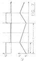
- FIG. 7 is a timing diagram of various signals produced by the precision oscillator as shown in FIG. 6.
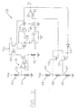
- a precision oscillator 30 in FIG. 2 is constructed with a reference current generator, a charge control stage, a capacitor, a comparator, and a voltage threshold generator.
- the reference current generator is constructed using resistors 32 , 34 , and 40 , amplifier 36 , N-channel transistor 38 , and P-- channel transistors 42 and 44 . More specifically, the first terminal of resistor 32 is connected to a voltage source Vdd and the second terminal of resistor 32 is connected to the noninverting input of amplifier 36 and the first terminal of resistor 34 . The second terminal of resistor 34 is connected to ground.
- the output of amplifier 36 is connected to the gate of transistor 38 .
- the source of transistor 38 is connected to the inverting input of amplifier 36 and to the first terminal of resistor 40 , the second terminal of resistor 40 is connected to ground.
- This configuration is commonly referred to as a voltage-follower since transistor 38 will be driven by amplifier 36 so that the voltage on resistor 40 follows the voltage on noninverting input of comparator 36 .
- the drain of transistor 38 is connected to a current mirror made from transistors 42 and 44 .
- the drain of transistor 38 is connected to the drain and gate of transistor 42 and the gate of transistor 44 .
- the sources of transistors 42 and 44 are connected to Vdd.
- the drain of transistor 44 is the mirrored current output of the current mirror and is also the output of the reference current generator.
- the charge control stage is constructed using P-channel transistors 50 and 52 , N-channel transistors 54 and 56 , and inverter 60 .
- the sources of transistors 50 and 52 are coupled together to form the input of the charge control stage and are therefore, coupled to the output of the reference current generator.
- the gate of transistor 50 is connected to the input of inverter 60 .
- the output of inverter 60 is connected to the gate of transistor 52 .
- the drain of transistor 50 is connected to the drain and gate of transistor 54 and to the gate of transistor 56 .
- the sources of transistors 54 and 56 are connected to ground.
- the drains of transistors 52 and 56 are connected together to form the output of the charge control stage. This output is connected to a first terminal of capacitor 58 and the inverting input of comparator 62 .
- the noninverting input of comparator 62 is connected to the output of the voltage threshold generator.
- the output of the comparator is the output of the oscillator and is connected to the input of inverter 60 , the gate of transistor 50 , and the gates of transistors 70 and 72 .
- the voltage threshold generator is constructed by connecting three resistors 64 , 66 and 68 in series across the supply voltage. These three resistors can be of equal value such that node 65 , between resistor 64 and 66 , has a voltage of approximately 2/3 the supply voltage. Similarly, the voltage at node 67 , between resistors 66 and 68 , has a voltage of approximately 1/3 the supply voltage. Alternate methods for generating two reference voltages will be known by persons skilled in the art.
- the source of transistor 70 is connected to node 65 .
- the source of transistor 72 is connected to node 67 .
- the gates of transistors 70 and 72 are connected to the output of inverter 74 .
- the input of inverter is connected to the output of comparator 62 .
- the drain of transistor 70 and the source of transistor 72 are connected together and to the noninverting input of comparator 62 .
- the charge control stage is used to direct the reference current generated from the reference current generator either to capacitor 58 or to remove the reference current from the capacitor. More specifically, when the output of comparator 62 is high, transistor 50 is turned off and transistor 52 is turned on. Therefore, the reference current from the reference current generator is conducted through transistor 52 onto capacitor 58 . Conversely, when the output of comparator 62 is low, transistor 50 is on and transistor 52 is turned off. Therefore, the reference current from the reference current generator is conducted through transistor 50 and therefore, through the current mirror made from transistors 54 and 56 . If the ratio between transistors 54 and 56 is approximately equal to one, a current approximately equal to the reference current will be discharged from capacitor 58 . In short; the charge control stage either charges capacitor 58 or discharges capacitor 58 responsive to the output of comparator 62 .
- the voltage threshold generator couples either the voltage at node 65 or the voltage at node 67 to the noninverting input of comparator 62 .
- the output of comparator 62 is high, the output of the inverter 74 is low so that transistor 70 is on and transistor 72 is turned off so that the voltage at node 65 is coupled to the noninverting input of comparator 62 .
- the voltage at node 67 is coupled to the noninverting input of comparator 62 when the output of comparator 62 is at a low voltage level which drives the output of inverter 74 high.
- an oscillation cycle begins at T 0 when the output of comparator 62 , Vo is at a low voltage level.
- the charge control stage is discharging capacitor 58 at a rate proportional to the reference current and inversely proportional to the size of the capacitor.
- the voltage on the capacitor, Vc is discharging at a constant rate.
- the noninverting input of comparator 62 is coupled to the voltage, V67 at node 67 .
- the comparator 62 switches to a high voltage state, as shown at T 1 . Consequently, the charge control stage begins to charge capacitor 58 and the voltage threshold generator changes the voltage threshold to the voltage at node 65 .
- comparator 62 When the voltage on capacitor 58 exceeds the voltage on node 65 comparator 62 will again change states such that the output is now again at a low voltage and the oscillation cycle will restart, as shown at T 2 .
- the frequency of oscillation is controlled by controlling reference current and the capacitance of C58 .
- FIG. 2 shows transistor 44 as the mirrored current stage of a current mirror in the reference current generator.
- FIG. 3 shows that transistor 44 of FIG. 2 can be a series of transistors coupled in parallel. More specifically, FIG. 3 shows the source of transistors 44' , 44" , 44'" , 44"" , and 44 n all connect to the source voltage Vdd. Similarly, the drains of transistors 44' , 44" , 44'" , 44"” , and 44 n are all connected together and form the output of the current mirror.
- the gate of transistor 44' would be connected to the gate and drain of transistor 42 of FIG. 2. Additionally, the gate of transistors 44' through 44 n can either be connect to Vdd or to the gate of transistor 44' .
- this circuit also provides the benefit of providing a precision oscillator which oscillates as a function of current (the reference current) instead of as a function of the supply voltage.
- FIG. 5 illustrates a speedometer system 80 which uses the precision oscillator 30 . More specifically, this figure shows a wheel sensor 82 coupled to an analog voltage converter 84 . The analog voltage converter 84 and precision oscillator are combined to drive the air core gauge motor 86 , which drives the speedometer display as is known in the art.
- the oscillator 30' illustratively includes a single capacitor 58' , a first or charging current source 90 , and a second or discharging current source 91 .
- the oscillator also includes a switch 93 for alternatingly switching the capacitor 58' to the charging current source 90 and then the discharging current source 91 . Accordingly, the switch 93 functions to alternatingly charge and discharge the capacitor 58' .
- the charging current source 90 is illustratively connected to a first supply voltage V dd
- the capacitor 58' is connected to a second supply voltage (ground) so that the charging current source is connectable in series with the capacitor between the first and second supply voltages by operation of the switch 93 .
- the discharging current source 91 is connected to the second supply voltage (ground) so that the discharge current source is connectable in parallel with the capacitor by the switch 93 .
- the charging current source 90 is preferably of a type having a current setting input for permitting setting of a charging current I 1 to the capacitor 58' as would be readily understood by those skilled in the art.
- the discharging current source 91 also preferably has a current setting input for permitting setting of a discharging current I 2 from the capacitor.
- a hysteretic comparator 95 is connected to the capacitor 58' for producing an oscillating signal responsive to alternatingly charging and discharging a voltage of the capacitor.
- the hysteretic comparator 95 will switch logic states at the upper and lower boundaries of the hysteresis band as will be readily understood by those skilled in the art. The further operation and construction of the hysteretic comparator 95 will be readily appreciated by those skilled in the art without further description herein.
- the oscillator 30' also preferably includes duty cycle control means 100 connected to the respective current setting inputs of the charging current source 90 and the discharging current source 91 for setting the respective charging current and the discharging current to thereby set a duty cycle of the oscillating signal from the hysteretic comparator 95 .
- the duty cycle control means 100 is provided by a processor 98 and a pair of digital-to-analog converters (D/As) 96 , 97 .
- the processor 98 may output a digital word to each D/A 96 , 97 , and, in turn, the D/As output signals S 1 , S 2 to the respective current setting inputs of the current sources 90 , 91 .
- the duty cycle of the oscillator 30' may be readily and precisely controlled.
- those of skill in the art will appreciate alternative arrangements for setting the duty cycle by controlling the currents I 1 , I 2 .
- one of the currents may be fixed by conventional circuit elements, while the other current is varied or controlled to achieve the desired duty cycle.
- a first enable signal En 1 is fed back to the charging current source 90 so that the source only operates when connected to the capacitor 58' by the switch 93 .
- a second enable signal En 2 is generated by the first illustrated inverter 101 and fed back to the second or discharging current source.
- a second inverter 102 is provided in the illustrated embodiment to further buffer the output as would be readily appreciated by those skilled in the art.
- either the En 1 or En 2 may be used to synchronize or control the switch 93 as would also be readily understood by those skilled in the art.
- the precision oscillator 30' also advantageously provides an output independent of the supply voltage V dd and using only a single capacitor 58' .
- the precision oscillator 30 ' also advantageously uses a hysteretic comparator 95 or Schmitt trigger, and provides duty cycle control means 100 for readily controlling the duty cycle of the oscillator.
- the charging time of the capacitor 58' is given by CV/I 1 , where C is the capacitance, and V is the hysteretic band, such as 2 volts, for example.
- the discharge time is given by CV/I 2 .
- the total time for a cycle (T) is given by the sum of charging and discharging times, and the output V o is high while the capacitor is being charged by the charging current I 1 and this defines the on time (t).
- the duty cycle is given by t/T. In the embodiment illustrated in FIG.
- the charging current I 1 is twice the discharging current I 2 , and the duty cycle (t/T) is therefore 33 percent.
- the duty cycle (t/T) is therefore 33 percent.
- other duty cycles may be readily and accurately determined.
- the hysteresis band V, and the capacitance C also affect the charging and discharging times.
- the embodiment of the precision oscillator 30' described above may be used in applications requiring an oscillating or clocking signal.
- the precision oscillator 30' may be used in the speedometer system 80 as shown in FIG. 5 and as described above.
- the precision oscillator 30' may be used in the speedometer system 80 as shown in FIG. 5 and as described above.
- Those of skill in the art will appreciate many other similar application. Accordingly, many modifications and other embodiments of the invention will come to the mind of one skilled in the art having the benefit of the teachings presented in the foregoing descriptions and the associated drawings. Therefore, it is to be understood that the invention is not to be limited to the specific embodiments disclosed, and that modifications and embodiments are intended to be included within the scope of the appended claims.
Landscapes
- Physics & Mathematics (AREA)
- General Physics & Mathematics (AREA)
- Dc-Dc Converters (AREA)
- Analogue/Digital Conversion (AREA)
- Inductance-Capacitance Distribution Constants And Capacitance-Resistance Oscillators (AREA)
Applications Claiming Priority (2)
| Application Number | Priority Date | Filing Date | Title |
|---|---|---|---|
| US08/862,946 US5990753A (en) | 1996-01-29 | 1997-05-30 | Precision oscillator circuit having a controllable duty cycle and related methods |
| US862946 | 1997-05-30 |
Publications (2)
| Publication Number | Publication Date |
|---|---|
| EP0881765A1 true EP0881765A1 (fr) | 1998-12-02 |
| EP0881765B1 EP0881765B1 (fr) | 2001-10-17 |
Family
ID=25339814
Family Applications (1)
| Application Number | Title | Priority Date | Filing Date |
|---|---|---|---|
| EP98303865A Expired - Lifetime EP0881765B1 (fr) | 1997-05-30 | 1998-05-15 | Circuit oscillateur de précision avec un facteur de marche ajustable et procédé associé |
Country Status (4)
| Country | Link |
|---|---|
| US (1) | US5990753A (fr) |
| EP (1) | EP0881765B1 (fr) |
| JP (1) | JPH11103239A (fr) |
| DE (1) | DE69802040T2 (fr) |
Cited By (5)
| Publication number | Priority date | Publication date | Assignee | Title |
|---|---|---|---|---|
| EP1117180A3 (fr) * | 2000-01-10 | 2004-06-23 | Research In Motion Limited | Circuit d'horloge avec réglage du rapport cyclique précis |
| US7504810B1 (en) * | 2005-02-18 | 2009-03-17 | National Semiconductor Corporation | Apparatus and method for generating a spread-spectrum clock for a switching regulator |
| EP1599775A4 (fr) * | 2003-03-03 | 2010-01-13 | Int Rectifier Corp | Oscillateur de ballast d'eclairage numerique |
| US8638162B2 (en) | 2010-09-27 | 2014-01-28 | Semiconductor Energy Laboratory Co., Ltd. | Reference current generating circuit, reference voltage generating circuit, and temperature detection circuit |
| WO2015134189A1 (fr) * | 2014-03-03 | 2015-09-11 | Qualcomm Incorporated | Systèmes et procédés de détection infrarouge |
Families Citing this family (49)
| Publication number | Priority date | Publication date | Assignee | Title |
|---|---|---|---|---|
| KR100277500B1 (ko) * | 1998-10-20 | 2001-01-15 | 김덕중 | 슈미트 트리거의 응답지연을 보상하는 주파수 발생 회로 |
| EP1049256A1 (fr) * | 1999-04-30 | 2000-11-02 | STMicroelectronics S.r.l. | Circuit oscillateur à tension d'alimentation basse, en particulier de type CMOS |
| US6404251B1 (en) * | 2000-03-27 | 2002-06-11 | Linear Technology Corporation | Systems and methods for linearly varying a pulse-width modulation signal with a control signal |
| US6369665B1 (en) * | 2000-10-02 | 2002-04-09 | Linear Technology Corporation | Maintaining constant amount of slope compensation regardless of switching frequency during synchronization |
| JP2002135086A (ja) * | 2000-10-27 | 2002-05-10 | Asahi Kasei Microsystems Kk | 発振器 |
| US6614375B2 (en) | 2001-09-19 | 2003-09-02 | Texas Instruments Incorporated | Sigma-delta analog-to-digital converter having improved reference multiplexer |
| DE10158113B4 (de) * | 2001-11-27 | 2004-09-02 | Texas Instruments Deutschland Gmbh | Multivibrator mit einem Komparator |
| US6590464B1 (en) * | 2002-03-13 | 2003-07-08 | Faraday Technology Corp. | Resistor-capacitor oscillator circuit |
| US6646513B1 (en) | 2002-08-28 | 2003-11-11 | Texas Instruments Incorporated | Oscillator circuit having an improved capacitor discharge circuit |
| DE10243197B4 (de) * | 2002-09-18 | 2011-05-05 | Infineon Technologies Ag | Digitales Signalübertragungsverfahren |
| WO2004055964A1 (fr) * | 2002-12-13 | 2004-07-01 | Orr Raymond K | Modulateur d'impulsions numerique programmable a commande de frequence numerique |
| EP2302850A1 (fr) * | 2003-04-30 | 2011-03-30 | Analog Devices, Inc. | Isolateurs de signal utilisant des micro-transformateurs |
| KR100510535B1 (ko) * | 2003-07-10 | 2005-08-26 | 삼성전자주식회사 | 전원 전압에 반비례하게 출력 신호의 주파수를 가변시키는오실레이터 |
| KR100549621B1 (ko) * | 2003-11-25 | 2006-02-03 | 주식회사 하이닉스반도체 | 셀프 리프래쉬용 오실레이터 |
| KR100587064B1 (ko) * | 2003-12-08 | 2006-06-07 | 주식회사 하이닉스반도체 | 가변 구동 전압을 갖는 오실레이타 |
| TWI229498B (en) * | 2004-01-09 | 2005-03-11 | Via Tech Inc | Low pass filter de-glitch circuit |
| JP4568595B2 (ja) * | 2004-12-10 | 2010-10-27 | 三菱電機株式会社 | 半導体回路 |
| EP2381577B1 (fr) * | 2005-02-28 | 2014-06-04 | Fujitsu Limited | Oscillateur commandé par un courant |
| JP4810132B2 (ja) * | 2005-06-15 | 2011-11-09 | 三洋電機株式会社 | 遅延回路およびリップルコンバータ |
| JP4881582B2 (ja) * | 2005-06-24 | 2012-02-22 | 三洋電機株式会社 | 遅延回路および駆動制御回路 |
| US7719305B2 (en) * | 2006-07-06 | 2010-05-18 | Analog Devices, Inc. | Signal isolator using micro-transformers |
| KR100779108B1 (ko) | 2006-08-22 | 2007-11-27 | 주식회사엘디티 | 발진 주파수 조절이 가능한 발진회로 |
| KR100887102B1 (ko) * | 2007-01-09 | 2009-03-04 | 삼성전기주식회사 | 듀얼모드 클럭 생성기 |
| US7667512B2 (en) * | 2007-03-29 | 2010-02-23 | Standard Microsystems Corporation | Duty cycle comparator |
| US7710054B2 (en) * | 2007-03-29 | 2010-05-04 | Standard Microsystems Corporation | Fan controller with duty cycle comparator |
| JP2008287387A (ja) * | 2007-05-16 | 2008-11-27 | Renesas Technology Corp | 非接触電子装置 |
| JP2009044646A (ja) * | 2007-08-10 | 2009-02-26 | Sanyo Electric Co Ltd | 電圧制御発振回路 |
| JP5120154B2 (ja) * | 2007-11-01 | 2013-01-16 | 株式会社デンソー | 信号形成回路 |
| JP5193590B2 (ja) * | 2007-12-27 | 2013-05-08 | ローム株式会社 | 発振回路 |
| JP2010183284A (ja) * | 2009-02-04 | 2010-08-19 | Toshiba Corp | 発振回路、及びメモリシステム |
| JP5389524B2 (ja) * | 2009-05-14 | 2014-01-15 | セミコンダクター・コンポーネンツ・インダストリーズ・リミテッド・ライアビリティ・カンパニー | 遅延回路 |
| US8242853B2 (en) * | 2010-02-02 | 2012-08-14 | Analog Devices, Inc. | Low headroom oscillator |
| CN102195466B (zh) * | 2010-03-02 | 2014-09-17 | 登丰微电子股份有限公司 | 抗噪声切换式转换电路及其控制器 |
| JP5588219B2 (ja) * | 2010-05-07 | 2014-09-10 | 株式会社東芝 | クロック生成回路 |
| WO2012029595A1 (fr) * | 2010-09-03 | 2012-03-08 | Semiconductor Energy Laboratory Co., Ltd. | Circuit d'oscillateur et élément à semi-conducteur utilisant le circuit d'oscillateur |
| CN101951177B (zh) * | 2010-09-06 | 2014-05-07 | Bcd半导体制造有限公司 | 开关电源系统及开关电源控制电路 |
| US8742858B2 (en) * | 2011-01-28 | 2014-06-03 | Infineon Technologies Ag | Relaxation oscillator having a supply voltage independent output frequency |
| CN102790601B (zh) * | 2012-08-08 | 2014-09-10 | 电子科技大学 | Rc振荡器 |
| US9293997B2 (en) | 2013-03-14 | 2016-03-22 | Analog Devices Global | Isolated error amplifier for isolated power supplies |
| CN103368528B (zh) * | 2013-07-26 | 2016-12-28 | 上海华虹宏力半导体制造有限公司 | 振荡器 |
| JP6153828B2 (ja) * | 2013-09-10 | 2017-06-28 | 日立オートモティブシステムズ株式会社 | 発振回路、それを用いた半導体集積回路装置および回転角検出装置 |
| US10270630B2 (en) | 2014-09-15 | 2019-04-23 | Analog Devices, Inc. | Demodulation of on-off-key modulated signals in signal isolator systems |
| US10536309B2 (en) | 2014-09-15 | 2020-01-14 | Analog Devices, Inc. | Demodulation of on-off-key modulated signals in signal isolator systems |
| US9660848B2 (en) | 2014-09-15 | 2017-05-23 | Analog Devices Global | Methods and structures to generate on/off keyed carrier signals for signal isolators |
| US9998301B2 (en) | 2014-11-03 | 2018-06-12 | Analog Devices, Inc. | Signal isolator system with protection for common mode transients |
| US10164614B2 (en) | 2016-03-31 | 2018-12-25 | Analog Devices Global Unlimited Company | Tank circuit and frequency hopping for isolators |
| EP3826179A1 (fr) * | 2019-11-22 | 2021-05-26 | Nexperia B.V. | Comparateur de tension à bascule de schmitt |
| CN111294023B (zh) * | 2020-04-24 | 2024-08-27 | 杭州思泰微电子有限公司 | 一种精确控制振荡器占空比的方法 |
| CN116527019B (zh) * | 2023-07-03 | 2023-12-05 | 成都芯翼科技有限公司 | 一种片内振荡器电路 |
Citations (4)
| Publication number | Priority date | Publication date | Assignee | Title |
|---|---|---|---|---|
| US4167699A (en) * | 1977-03-25 | 1979-09-11 | Stewart-Warner Corporation | User calibrated electronic speedometer and odometer |
| US4904960A (en) * | 1989-04-10 | 1990-02-27 | National Semiconductor Corporation | Precision CMOS oscillator circuit |
| US5459437A (en) * | 1994-05-10 | 1995-10-17 | Integrated Device Technology | Logic gate with controllable hysteresis and high frequency voltage controlled oscillator |
| US5614871A (en) * | 1995-01-25 | 1997-03-25 | Nippon Precision Circuits Inc. | Voltage-controlled oscillator circuit |
Family Cites Families (18)
| Publication number | Priority date | Publication date | Assignee | Title |
|---|---|---|---|---|
| US4365212A (en) * | 1980-09-30 | 1982-12-21 | Rca Corporation | Gated oscillator including initialization apparatus for enhancing periodicity |
| JPS59165516A (ja) * | 1983-03-09 | 1984-09-18 | Yokogawa Hokushin Electric Corp | 無安定マルチバイブレ−タ |
| US4594565A (en) * | 1984-08-30 | 1986-06-10 | Cordis Corporation | Clock oscillator for a cardiac pacer having frequency compensation for temperature and voltage fluctuations |
| EP0231872B1 (fr) * | 1986-02-03 | 1992-06-10 | Siemens Aktiengesellschaft | Source de courant commutée |
| JPS62260420A (ja) * | 1986-04-28 | 1987-11-12 | シ−メンス、アクチエンゲゼルシヤフト | 集積nmos回路装置 |
| US4723114A (en) * | 1986-07-07 | 1988-02-02 | Texas Instruments Incorporated | Method and circuit for trimming the frequency of an oscillator |
| JPH0334619A (ja) * | 1989-06-29 | 1991-02-14 | Nec Corp | Cr型発振回路 |
| FR2649505B1 (fr) * | 1989-07-07 | 1991-10-25 | Sgs Thomson Microelectronics | Circuit integre avec oscillateur reglable a frequence independante de la tension d'alimentation |
| JP2990863B2 (ja) * | 1991-06-26 | 1999-12-13 | 日本電気株式会社 | 発振回路 |
| GB2268647B (en) * | 1992-07-02 | 1996-04-10 | Motorola Inc | Voltage controlled oscillator |
| DE4306950C2 (de) * | 1993-03-05 | 1997-04-10 | Balluff Gebhard Feinmech | Elektronisches Zweidrahtschaltgerät |
| DE4340924C2 (de) * | 1993-12-01 | 1995-10-05 | Telefunken Microelectron | Frequenzstabiler RC-Oszillator |
| JP3456041B2 (ja) * | 1995-01-12 | 2003-10-14 | 株式会社デンソー | センサ信号処理装置 |
| US5508664A (en) * | 1995-04-20 | 1996-04-16 | International Business Machines Corporation | Oscillators having charge/discharge circuits with adjustment to maintain desired duty cycles |
| JP3541509B2 (ja) * | 1995-07-28 | 2004-07-14 | 株式会社デンソー | 波形整形装置 |
| DE19536840A1 (de) * | 1995-10-02 | 1997-04-03 | Asea Brown Boveri | Verfahren zur Drehzahlmessung |
| US5638031A (en) * | 1996-01-29 | 1997-06-10 | Sgs-Thomson Microelectronics, Inc. | Precision oscillator circuit |
| US5740083A (en) * | 1996-04-01 | 1998-04-14 | Ford Motor Company | Delta time measurement circuit for determining parameter derivatives of a rotational velocity sensor signal |
-
1997
- 1997-05-30 US US08/862,946 patent/US5990753A/en not_active Expired - Lifetime
-
1998
- 1998-05-15 DE DE69802040T patent/DE69802040T2/de not_active Expired - Fee Related
- 1998-05-15 EP EP98303865A patent/EP0881765B1/fr not_active Expired - Lifetime
- 1998-05-29 JP JP10150428A patent/JPH11103239A/ja active Pending
Patent Citations (4)
| Publication number | Priority date | Publication date | Assignee | Title |
|---|---|---|---|---|
| US4167699A (en) * | 1977-03-25 | 1979-09-11 | Stewart-Warner Corporation | User calibrated electronic speedometer and odometer |
| US4904960A (en) * | 1989-04-10 | 1990-02-27 | National Semiconductor Corporation | Precision CMOS oscillator circuit |
| US5459437A (en) * | 1994-05-10 | 1995-10-17 | Integrated Device Technology | Logic gate with controllable hysteresis and high frequency voltage controlled oscillator |
| US5614871A (en) * | 1995-01-25 | 1997-03-25 | Nippon Precision Circuits Inc. | Voltage-controlled oscillator circuit |
Non-Patent Citations (1)
| Title |
|---|
| ANONYMOUS: "Variable Frequency Oscillator for Switching Regulator Control. May 1977.", IBM TECHNICAL DISCLOSURE BULLETIN, vol. 19, no. 12, May 1977 (1977-05-01), NEW YORK, US, pages 4652 - 4653, XP002072278 * |
Cited By (9)
| Publication number | Priority date | Publication date | Assignee | Title |
|---|---|---|---|---|
| EP1117180A3 (fr) * | 2000-01-10 | 2004-06-23 | Research In Motion Limited | Circuit d'horloge avec réglage du rapport cyclique précis |
| US6915442B2 (en) | 2000-01-10 | 2005-07-05 | Research In Motion Limited | Precision-controlled duty cycle clock circuit |
| EP1599775A4 (fr) * | 2003-03-03 | 2010-01-13 | Int Rectifier Corp | Oscillateur de ballast d'eclairage numerique |
| US7504810B1 (en) * | 2005-02-18 | 2009-03-17 | National Semiconductor Corporation | Apparatus and method for generating a spread-spectrum clock for a switching regulator |
| US8638162B2 (en) | 2010-09-27 | 2014-01-28 | Semiconductor Energy Laboratory Co., Ltd. | Reference current generating circuit, reference voltage generating circuit, and temperature detection circuit |
| WO2015134189A1 (fr) * | 2014-03-03 | 2015-09-11 | Qualcomm Incorporated | Systèmes et procédés de détection infrarouge |
| KR20160119270A (ko) * | 2014-03-03 | 2016-10-12 | 퀄컴 인코포레이티드 | 주파수 검출을 위한 시스템들 및 방법들 |
| CN106063207A (zh) * | 2014-03-03 | 2016-10-26 | 高通股份有限公司 | 用于频率检测的系统和方法 |
| CN106063207B (zh) * | 2014-03-03 | 2018-01-05 | 高通股份有限公司 | 用于频率检测的系统和方法 |
Also Published As
| Publication number | Publication date |
|---|---|
| JPH11103239A (ja) | 1999-04-13 |
| EP0881765B1 (fr) | 2001-10-17 |
| US5990753A (en) | 1999-11-23 |
| DE69802040T2 (de) | 2002-07-04 |
| DE69802040D1 (de) | 2001-11-22 |
Similar Documents
| Publication | Publication Date | Title |
|---|---|---|
| EP0881765B1 (fr) | Circuit oscillateur de précision avec un facteur de marche ajustable et procédé associé | |
| JP3053437B2 (ja) | 高精度rc発振器 | |
| US11245360B2 (en) | Oscillator circuit, chip and electronic device | |
| US5245524A (en) | DC-DC converter of charge pump type | |
| JP3284341B2 (ja) | 発振回路 | |
| US4428040A (en) | Low power consumption electronic circuit | |
| US7425857B2 (en) | Time-delay circuit | |
| US5638031A (en) | Precision oscillator circuit | |
| CN108123703B (zh) | 无带隙基准的自偏置集成振荡器 | |
| US20060126238A1 (en) | Semiconductor circuit for use in timer circuit or oscillator circuit | |
| US5760655A (en) | Stable frequency oscillator having two capacitors that are alternately charged and discharged | |
| JP3963421B2 (ja) | 制御発振システムとその方法 | |
| EP2887545A1 (fr) | Circuit oscillateur | |
| JP2003008410A (ja) | 遅延回路 | |
| US6552622B1 (en) | Oscillator having reduced sensitivity to supply voltage changes | |
| JPH06224705A (ja) | 発振回路 | |
| CN108649900B (zh) | 一种振荡器链路延时校正电路 | |
| EP1564886A1 (fr) | Circuit à retard de temps | |
| JPH0810816B2 (ja) | 発振回路 | |
| JP3284340B2 (ja) | 発振回路 | |
| JP3671773B2 (ja) | 発振回路 | |
| JPH09107273A (ja) | パルス発振器 | |
| US20250211210A1 (en) | Oscillator circuit | |
| JP3392278B2 (ja) | 発振器 | |
| JP3304926B2 (ja) | 電圧補正発振装置及び発振周波数の制御方法 |
Legal Events
| Date | Code | Title | Description |
|---|---|---|---|
| PUAI | Public reference made under article 153(3) epc to a published international application that has entered the european phase |
Free format text: ORIGINAL CODE: 0009012 |
|
| AK | Designated contracting states |
Kind code of ref document: A1 Designated state(s): DE FR GB IT |
|
| AX | Request for extension of the european patent |
Free format text: AL;LT;LV;MK;RO;SI |
|
| RAP3 | Party data changed (applicant data changed or rights of an application transferred) |
Owner name: STMICROELECTRONICS, INC. |
|
| 17P | Request for examination filed |
Effective date: 19990527 |
|
| AKX | Designation fees paid |
Free format text: DE FR GB IT |
|
| 17Q | First examination report despatched |
Effective date: 19990923 |
|
| GRAG | Despatch of communication of intention to grant |
Free format text: ORIGINAL CODE: EPIDOS AGRA |
|
| GRAG | Despatch of communication of intention to grant |
Free format text: ORIGINAL CODE: EPIDOS AGRA |
|
| GRAH | Despatch of communication of intention to grant a patent |
Free format text: ORIGINAL CODE: EPIDOS IGRA |
|
| GRAH | Despatch of communication of intention to grant a patent |
Free format text: ORIGINAL CODE: EPIDOS IGRA |
|
| GRAA | (expected) grant |
Free format text: ORIGINAL CODE: 0009210 |
|
| AK | Designated contracting states |
Kind code of ref document: B1 Designated state(s): DE FR GB IT |
|
| PG25 | Lapsed in a contracting state [announced via postgrant information from national office to epo] |
Ref country code: IT Free format text: LAPSE BECAUSE OF FAILURE TO SUBMIT A TRANSLATION OF THE DESCRIPTION OR TO PAY THE FEE WITHIN THE PRESCRIBED TIME-LIMIT;WARNING: LAPSES OF ITALIAN PATENTS WITH EFFECTIVE DATE BEFORE 2007 MAY HAVE OCCURRED AT ANY TIME BEFORE 2007. THE CORRECT EFFECTIVE DATE MAY BE DIFFERENT FROM THE ONE RECORDED. Effective date: 20011017 |
|
| REF | Corresponds to: |
Ref document number: 69802040 Country of ref document: DE Date of ref document: 20011122 |
|
| REG | Reference to a national code |
Ref country code: GB Ref legal event code: IF02 |
|
| ET | Fr: translation filed | ||
| PLBE | No opposition filed within time limit |
Free format text: ORIGINAL CODE: 0009261 |
|
| STAA | Information on the status of an ep patent application or granted ep patent |
Free format text: STATUS: NO OPPOSITION FILED WITHIN TIME LIMIT |
|
| 26N | No opposition filed | ||
| PGFP | Annual fee paid to national office [announced via postgrant information from national office to epo] |
Ref country code: DE Payment date: 20040527 Year of fee payment: 7 |
|
| PG25 | Lapsed in a contracting state [announced via postgrant information from national office to epo] |
Ref country code: DE Free format text: LAPSE BECAUSE OF NON-PAYMENT OF DUE FEES Effective date: 20051201 |
|
| PGFP | Annual fee paid to national office [announced via postgrant information from national office to epo] |
Ref country code: GB Payment date: 20080521 Year of fee payment: 11 |
|
| GBPC | Gb: european patent ceased through non-payment of renewal fee |
Effective date: 20090515 |
|
| REG | Reference to a national code |
Ref country code: FR Ref legal event code: ST Effective date: 20100129 |
|
| PG25 | Lapsed in a contracting state [announced via postgrant information from national office to epo] |
Ref country code: FR Free format text: LAPSE BECAUSE OF NON-PAYMENT OF DUE FEES Effective date: 20090602 |
|
| PGFP | Annual fee paid to national office [announced via postgrant information from national office to epo] |
Ref country code: FR Payment date: 20080514 Year of fee payment: 11 |
|
| PG25 | Lapsed in a contracting state [announced via postgrant information from national office to epo] |
Ref country code: GB Free format text: LAPSE BECAUSE OF NON-PAYMENT OF DUE FEES Effective date: 20090515 |