EP0883182A2 - Gitteranordnung der Elektroden auf einer Mehrlagenleiterplatte - Google Patents
Gitteranordnung der Elektroden auf einer Mehrlagenleiterplatte Download PDFInfo
- Publication number
- EP0883182A2 EP0883182A2 EP98304446A EP98304446A EP0883182A2 EP 0883182 A2 EP0883182 A2 EP 0883182A2 EP 98304446 A EP98304446 A EP 98304446A EP 98304446 A EP98304446 A EP 98304446A EP 0883182 A2 EP0883182 A2 EP 0883182A2
- Authority
- EP
- European Patent Office
- Prior art keywords
- lands
- circuit
- land
- patterns
- layer
- Prior art date
- Legal status (The legal status is an assumption and is not a legal conclusion. Google has not performed a legal analysis and makes no representation as to the accuracy of the status listed.)
- Granted
Links
Images


Classifications
-
- H—ELECTRICITY
- H05—ELECTRIC TECHNIQUES NOT OTHERWISE PROVIDED FOR
- H05K—PRINTED CIRCUITS; CASINGS OR CONSTRUCTIONAL DETAILS OF ELECTRIC APPARATUS; MANUFACTURE OF ASSEMBLAGES OF ELECTRICAL COMPONENTS
- H05K3/00—Apparatus or processes for manufacturing printed circuits
- H05K3/46—Manufacturing multilayer circuits
- H05K3/4697—Manufacturing multilayer circuits having cavities, e.g. for mounting components
-
- H—ELECTRICITY
- H05—ELECTRIC TECHNIQUES NOT OTHERWISE PROVIDED FOR
- H05K—PRINTED CIRCUITS; CASINGS OR CONSTRUCTIONAL DETAILS OF ELECTRIC APPARATUS; MANUFACTURE OF ASSEMBLAGES OF ELECTRICAL COMPONENTS
- H05K1/00—Printed circuits
- H05K1/02—Details
- H05K1/11—Printed elements for providing electric connections to or between printed circuits
- H05K1/111—Pads for surface mounting, e.g. lay-out
- H05K1/112—Pads for surface mounting, e.g. lay-out directly combined with via connections
-
- H—ELECTRICITY
- H05—ELECTRIC TECHNIQUES NOT OTHERWISE PROVIDED FOR
- H05K—PRINTED CIRCUITS; CASINGS OR CONSTRUCTIONAL DETAILS OF ELECTRIC APPARATUS; MANUFACTURE OF ASSEMBLAGES OF ELECTRICAL COMPONENTS
- H05K1/00—Printed circuits
- H05K1/02—Details
- H05K1/11—Printed elements for providing electric connections to or between printed circuits
- H05K1/115—Via connections; Lands around holes or via connections
- H05K1/116—Lands, clearance holes or other lay-out details concerning the surrounding of a via
-
- H—ELECTRICITY
- H05—ELECTRIC TECHNIQUES NOT OTHERWISE PROVIDED FOR
- H05K—PRINTED CIRCUITS; CASINGS OR CONSTRUCTIONAL DETAILS OF ELECTRIC APPARATUS; MANUFACTURE OF ASSEMBLAGES OF ELECTRICAL COMPONENTS
- H05K1/00—Printed circuits
- H05K1/18—Printed circuits structurally associated with non-printed electric components
- H05K1/182—Printed circuits structurally associated with non-printed electric components associated with components mounted in printed circuit boards [PCB], e.g. insert-mounted components [IMC]
- H05K1/185—Printed circuits structurally associated with non-printed electric components associated with components mounted in printed circuit boards [PCB], e.g. insert-mounted components [IMC] associated with components encapsulated in the insulating substrate of the PCBs; associated with components incorporated in internal layers of multilayer circuit boards
-
- H—ELECTRICITY
- H05—ELECTRIC TECHNIQUES NOT OTHERWISE PROVIDED FOR
- H05K—PRINTED CIRCUITS; CASINGS OR CONSTRUCTIONAL DETAILS OF ELECTRIC APPARATUS; MANUFACTURE OF ASSEMBLAGES OF ELECTRICAL COMPONENTS
- H05K3/00—Apparatus or processes for manufacturing printed circuits
- H05K3/40—Forming printed elements for providing electric connections to or between printed circuits
- H05K3/42—Plated through-holes or plated via connections
- H05K3/429—Plated through-holes specially for multilayer circuits, e.g. having connections to inner circuit layers
-
- H—ELECTRICITY
- H10—SEMICONDUCTOR DEVICES; ELECTRIC SOLID-STATE DEVICES NOT OTHERWISE PROVIDED FOR
- H10W—GENERIC PACKAGES, INTERCONNECTIONS, CONNECTORS OR OTHER CONSTRUCTIONAL DETAILS OF DEVICES COVERED BY CLASS H10
- H10W70/00—Package substrates; Interposers; Redistribution layers [RDL]
- H10W70/60—Insulating or insulated package substrates; Interposers; Redistribution layers
- H10W70/62—Insulating or insulated package substrates; Interposers; Redistribution layers characterised by their interconnections
- H10W70/63—Vias, e.g. via plugs
- H10W70/635—Through-vias
-
- H—ELECTRICITY
- H10—SEMICONDUCTOR DEVICES; ELECTRIC SOLID-STATE DEVICES NOT OTHERWISE PROVIDED FOR
- H10W—GENERIC PACKAGES, INTERCONNECTIONS, CONNECTORS OR OTHER CONSTRUCTIONAL DETAILS OF DEVICES COVERED BY CLASS H10
- H10W70/00—Package substrates; Interposers; Redistribution layers [RDL]
- H10W70/60—Insulating or insulated package substrates; Interposers; Redistribution layers
- H10W70/62—Insulating or insulated package substrates; Interposers; Redistribution layers characterised by their interconnections
- H10W70/65—Shapes or dispositions of interconnections
-
- H—ELECTRICITY
- H05—ELECTRIC TECHNIQUES NOT OTHERWISE PROVIDED FOR
- H05K—PRINTED CIRCUITS; CASINGS OR CONSTRUCTIONAL DETAILS OF ELECTRIC APPARATUS; MANUFACTURE OF ASSEMBLAGES OF ELECTRICAL COMPONENTS
- H05K1/00—Printed circuits
- H05K1/02—Details
- H05K1/0296—Conductive pattern lay-out details not covered by sub groups H05K1/02 - H05K1/0295
- H05K1/0298—Multilayer circuits
-
- H—ELECTRICITY
- H05—ELECTRIC TECHNIQUES NOT OTHERWISE PROVIDED FOR
- H05K—PRINTED CIRCUITS; CASINGS OR CONSTRUCTIONAL DETAILS OF ELECTRIC APPARATUS; MANUFACTURE OF ASSEMBLAGES OF ELECTRICAL COMPONENTS
- H05K2201/00—Indexing scheme relating to printed circuits covered by H05K1/00
- H05K2201/09—Shape and layout
- H05K2201/09209—Shape and layout details of conductors
- H05K2201/09218—Conductive traces
- H05K2201/09227—Layout details of a plurality of traces, e.g. escape layout for Ball Grid Array [BGA] mounting
-
- H—ELECTRICITY
- H05—ELECTRIC TECHNIQUES NOT OTHERWISE PROVIDED FOR
- H05K—PRINTED CIRCUITS; CASINGS OR CONSTRUCTIONAL DETAILS OF ELECTRIC APPARATUS; MANUFACTURE OF ASSEMBLAGES OF ELECTRICAL COMPONENTS
- H05K2201/00—Indexing scheme relating to printed circuits covered by H05K1/00
- H05K2201/10—Details of components or other objects attached to or integrated in a printed circuit board
- H05K2201/10613—Details of electrical connections of non-printed components, e.g. special leads
- H05K2201/10621—Components characterised by their electrical contacts
- H05K2201/10734—Ball grid array [BGA]; Bump grid array
-
- H—ELECTRICITY
- H10—SEMICONDUCTOR DEVICES; ELECTRIC SOLID-STATE DEVICES NOT OTHERWISE PROVIDED FOR
- H10W—GENERIC PACKAGES, INTERCONNECTIONS, CONNECTORS OR OTHER CONSTRUCTIONAL DETAILS OF DEVICES COVERED BY CLASS H10
- H10W70/00—Package substrates; Interposers; Redistribution layers [RDL]
- H10W70/60—Insulating or insulated package substrates; Interposers; Redistribution layers
- H10W70/62—Insulating or insulated package substrates; Interposers; Redistribution layers characterised by their interconnections
- H10W70/65—Shapes or dispositions of interconnections
- H10W70/654—Top-view layouts
- H10W70/655—Fan-out layouts
-
- H—ELECTRICITY
- H10—SEMICONDUCTOR DEVICES; ELECTRIC SOLID-STATE DEVICES NOT OTHERWISE PROVIDED FOR
- H10W—GENERIC PACKAGES, INTERCONNECTIONS, CONNECTORS OR OTHER CONSTRUCTIONAL DETAILS OF DEVICES COVERED BY CLASS H10
- H10W72/00—Interconnections or connectors in packages
- H10W72/071—Connecting or disconnecting
- H10W72/072—Connecting or disconnecting of bump connectors
- H10W72/07251—Connecting or disconnecting of bump connectors characterised by changes in properties of the bump connectors during connecting
-
- H—ELECTRICITY
- H10—SEMICONDUCTOR DEVICES; ELECTRIC SOLID-STATE DEVICES NOT OTHERWISE PROVIDED FOR
- H10W—GENERIC PACKAGES, INTERCONNECTIONS, CONNECTORS OR OTHER CONSTRUCTIONAL DETAILS OF DEVICES COVERED BY CLASS H10
- H10W72/00—Interconnections or connectors in packages
- H10W72/20—Bump connectors, e.g. solder bumps or copper pillars; Dummy bumps; Thermal bumps
Definitions
- the present invention relates to a multi-layer circuit board for mounting an electronic part such as a semiconductor chip or a semiconductor device having a number of electrodes arranged in a lattice form or in a staggered manner.
- Fig. 25 illustrates a prior art or mounting a semiconductor chip 4 on a substrate 5 relying on a flip chip connection.
- the semiconductor chip 4 shown here has electrodes 6 arranged on the outer peripheral edges thereof. Circuit patterns 7 are connected to the electrodes 6 and are taken out; i.e., the circuit patterns 7 are connected to every electrode 6 on a surface.
- Fig. 24 illustrates the arrangement of lands on a wiring member for mounting a semiconductor chip having two rows of electrodes 6 arranged along the outer peripheral edges of the electrode-forming surface, and the arrangement of circuit patterns 7 connected to the lands 8.
- each circuit pattern 7 is drawn from an intermediate portion of the land 8; i.e., the circuit pattern 7 is taken out from every land 8 on a plane.
- FIG. 26 illustrates an example where a semiconductor chip 4 is mounted on a multi-layer circuit board obtained by laminating a plurality of layers.
- a semiconductor chip 4 is mounted on a multi-layer circuit board obtained by laminating a plurality of layers.
- reference numeral 7a denotes a circuit pattern of an inner layer
- 5a to 5d denote circuit boards which are the first to fourth layers.
- the semiconductor chip having electrodes arranged like an array When the semiconductor chip having electrodes arranged like an array is to be mounted on the circuit board, about two circuit boards may be laminated one upon the other provided the number of the electrodes is not very large.
- the semiconductor chip has as many pins as, for example, 30 ⁇ 30 pins or 40 ⁇ 40 pins, however, the circuit boards must be laminated in 6 to 10 layers.
- circuit boards in which the circuit patterns are very densely formed are to be laminated in many layers, there will be employed a high-density wiring method such as build-up method accompanied, however, by serious problems in regard to yield of the products, reliability and the cost of production. That is, when the circuit patterns are to be formed in many layers, vias are formed in each layer to accomplish an electric connection between the circuit patterns and the circuit patterns across the layer, and the layers are successively laminated, requiring a high degree of precision without, however, offering high degree of reliability. When many layers are laminated, furthermore, it is required that none of the layers is defective, involving further increased technical difficulty.
- the present invention is concerned with a multi-layer circuit board for mounting an electronic part such as a semiconductor chip having as many as 40 ⁇ 40 pins arranged in an array on the side of the mounting surface or a semiconductor device having electrodes arranged in an array on the side of the mounting surface.
- the object of the present invention is to provide a multi-layer circuit board which makes it possible to mount an electronic part such as a semiconductor chip or a semiconductor device, despite a decreased number of circuit boards being laminated one upon the other, which features improved yield of production and which can be used as a highly reliable product.
- the present invention provides the following multi-layer circuit board.
- the present invention provides a multi-layer circuit board formed by e.g., laminating a plurality of layers in order to mount an electronic part such as a semiconductor chip or a semiconductor device having many electrodes arranged in the form of an array.
- a multi-layer circuit board can be constituted by forming the circuit boards (wiring layers) in a decreased number of layers.
- various methods such as a build-up method, can be employed.
- Arrangements of electrodes of the electronic parts can be divided into a normal lattice arrangement and a staggered lattice arrangement.
- the electrodes when the electrodes are arranged in the normal lattice form or staggered lattice form, a problem arises in regard to how the circuit patterns can be arranged to accomplish the highest efficiency.
- the circuit patterns pass through among the lands.
- the circuit patterns must be set depending upon the predetermined conditions such as pitch of lands, diameter of lands, width of patterns and gap between the patterns.
- the following method is employed for determining the arrangement of circuit patterns on each circuit board in a multi-layer circuit board formed by laminating the circuit boards. Upon arranging the circuit patterns according to this method, it is possible to form a multi-layer circuit board in the least number of layers.
- m ⁇ (land pitch) ⁇ (n - 1) - (land diameter) - (space between patterns) ⁇ ⁇ (pattern width + space between patterns) where land pitch is a distance between the centers of the lands, land diameter is a diameter of the land, and space between patterns is a minimum distance that must be maintained between the neighboring circuit patterns.
- a minimum integer that gives m ⁇ (k + 1) is selected as a parameter, and the circuit patterns are arranged according to the value n.
- a value m is found from the conditions of a given land pitch, land diameter and pattern width, and is compared with (k + 1) to find a minimum value n (integerj that gives m ⁇ (k + 1). Then, the conditions are found that remove the land sequences of a number of (n - 2) for the value n, and the circuit patterns are preferentially drawn from the land sequences of the number of (n - 2) to accomplish an optimum arrangement.
- the distance L - L represents two land pitches.
- three circuit patterns can be arranged, i,e., a circuit pattern drawn from an intermediate land and two circuit patterns passing through the two lands sandwiched by the lands on both sides and the intermediate land.
- the land pitch, land diameter, pattern width and space between patterns have been determined in advance, and it is easy to find the values m and (k + 1) based on these values with n as a parameter. Based upon the calculated results, it can be easily determined which arrangement of circuit patterns would be efficient.
- the circuit patterns on each circuit layer are designed by commonly setting the positions of land sequences (that are to be removed) from where the circuit patterns are to be drawn on each of the layers, and for the land sequences from where the circuit patterns are drawn on the preceding layer, the circuit patterns are also drawn from the same land sequences even on the next layer.
- the values m and (k + 1) found with n as a parameter are compared with each other to determine a minimum value n (integer) that gives m ⁇ (k + 1), conditions are determined based on the number of n for selectively subtracting the circuit patterns from the land sequences of the number of (n - 2), and the land sequences are erased depending upon the conditions, in order to efficiently design the circuit patterns. That is, the idea for arranging a single circuit pattern can be adapted even under the condition where a plurality of circuit patterns are arranged between the neighboring lands (in the channel portion), in order to efficiently design the circuit patterns.
- the lands to be selected are those lands that remain when the lands at both ends are removed from the lands of the number of n.
- the method of arranging the circuit patterns adapted to the above-mentioned case of normal lattice arrangement can be adapted, too, to the case where the lands are arranged in the staggered lattice form. That is, the staggered lattice arrangement can be regarded to be a lattice arrangement when viewed from a diagonal direction. Therefore, this arrangement is regarded to be the lattice arrangement as viewed from the diagonal direction, and there can be adapted the same as the lattice arrangement.
- values m and (k + 1) are found from the land pitch, land diameter, pattern width, and space between patterns using n as a parameter, and an effective value n is found therefrom, and the land sequences are determined depending upon the value n for preferentially drawing the circuit patterns based on the same idea as that of the case of the lattice arrangement.
- the method of the present invention can be effectively adapted to the case where it is possible to pass only one circuit pattern between the neighboring lands and the electrode arrangement is not smaller than 6 ⁇ 6.
- the electrodes are arranged according to the normal lattice arrangement or the normal staggered lattice arrangement while maintaining an equal distance in the vertical and lateral directions.
- the idea of the present invention can be adapted even to a semiconductor chip having pitches of arrangements that are slightly different in the vertical and lateral directions.
- Described below is a multi-layer circuit board for mounting an electronic part having electrodes arranged in the form of a normal lattice of 30 ⁇ 30 pins, the circuit patterns being arranged under the following conditions.
- the circuit patterns are so arranged as to preferentially draw a circuit pattern from an intermediate land among the three lands, in order to accomplish an efficient arrangement.
- Figs. 2 to 5 illustrate an example for forming circuit patterns on each of the first to fifth layers in the case of the above-mentioned electrode arrangement.
- the first layer is the one to which the semiconductor chip is joined, arid the second to fifth layers are successively laminated on the first layer.
- the drawings illustrate the arrangement of all terminals of 30 x 30 pins.
- the lands 10 joined to every electrode are provided in the same arrangement as that of the electrodes of the electronic part.
- circuit patterns 7 are so drawn as to erase every other sequences of lands 10. Therefore, all circuit patterns 7 are drawn from the lands of the outermost circumference, and land sequences are so set as to preferentially draw every other sequences of circuit patterns 7 on each side.
- the lands to which no circuit pattern 7 is connected on the first layer are electrically connected to the second layer through vias.
- Fig. 3 illustrates how to draw the circuit patterns 7 on the second layer.
- the circuit patterns 7 on the second layer are drawn in the same manner as on the first layer.
- the circuit patterns 7 are drawn from the lands 10 of the inner side of the land sequence at the same position as the land sequence from which the circuit patterns 7 are preferentially drawn on the first layer.
- the region for arranging the lands 10 from where the circuit patterns 7 are drawn on the first layer can be utilized as space for drawing the circuit patterns, making it possible to draw circuit patterns 7 from the lands 10 of more inner side on the second layer.
- Reference numeral 11a denotes a land from where the circuit pattern 7 is drawn on the second layer
- 11b denotes a land from where no circuit pattern 7 is drawn.
- the lands 11b are electrically connected to the lands 10b on the first layer through vias.
- Fig. 4 illustrates how to draw the circuit patterns 7 on the third layer.
- the circuit patterns 7 on the third layer are drawn in the same manner as on the first layer and on the second layer.
- the circuit patterns 7 are drawn from the inner side of the sequences from where the circuit patterns are preferentially drawn. In this case, too, the circuit patterns 7 are drawn from the three lands on the same sequence.
- Reference numeral 12a denotes a land from where the circuit pattern 7 is drawn on the third layer
- 12b denotes a land from where no circuit pattern 7 is drawn.
- the lands 12b are electrically connected to the lands 10 on the first layer and on the second layer.
- Fig. 5 illustrates how to draw the circuit patterns 7 on the fourth layer
- Fig. 6 illustrates how to draw the circuit patterns 7 on the fifth layer.
- the circuit patterns 7 on the fourth layer and on the fifth layer are drawn in the same manner as on the first to third layers.
- reference numeral 13a denotes a land from where the circuit pattern 7 is drawn
- 13b denotes a land from where no circuit pattern 7 is drawn.
- the lands 13b are electrically connected to the lands 10 on the first, second and third layers.
- reference numeral 14a denote a land from where the circuit pattern 7 is drawn.
- the circuit patterns 7 are drawn from every land.
- the circuit patterns are drawn from every electrode by using circuit boards in five layers. Seven layers will be required when the circuit patterns are drawn from the two lands of the outer side on each of the layers according to the method shown in Fig. 24.
- a multi-layer circuit board for mounting an electronic part having electrodes arranged in the form of a normal lattice of 30 x 30 pins, the circuit patterns 7 being arranged under the following conditions.
- Figs. 7 to 11 illustrate an example in which the circuit patterns 7 are arranged being drawn from the lands 10 according to the above-mentioned arrangement standard.
- Figs. 7 to 11 illustrate one-fourth of the 30 x 30 pin arrangement.
- Fig. 7 illustrates the arrangements of circuit patterns 7 on the first layer.
- the circuit patterns 7 are preferentially drawn from the intermediate two lands 10 among the four lands 10.
- arrows indicate the positions of land sequences from where the circuit patterns are preferentially drawn. Two arrows are arranged after every other two sequences.
- the land sequences from where the circuit patterns 7 are preferentially drawn are arranged after every other two sequences.
- the circuit patterns 7 are drawn from the three lands as in the above-mentioned embodiment.
- Fig. 8 illustrates the arrangement of circuit patterns 7 on the second layer. Even cn the second layer, the circuit patterns 7 are preferentially drawn from the predetermined land sequences (arrows) for preferentially drawing the circuit patterns 7, and six circuit patterns 7 can be drawn on the region where the circuit patterns have already been drawn on the first layer. Therefore, the circuit patterns 7 are arranged under these conditions.
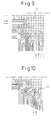
- Fig. 9 illustrates the arrangement of circuit patterns on the third layer
- Fig. 10 illustrates the arrangement of circuit patterns on the fourth layer
- Fig. 11 illustrates the arrangement of circuit patterns on the fifth layer.
- the circuit patterns 7 are drawn from the land sequences at predetermined positions for preferentially drawing the circuit patterns.
- the circuit patterns 7 are successively drawn from the lands 10 positioned on the outer side. Therefore, a land 10 near the corner is drawn first among the lands 10 arranged in the normal lattice form. Therefore, the circuit pattern 7 may be drawn in any direction irrespective of the above-mentioned conditions from the land 10 arranged near the corner.
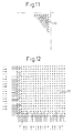
- a multi-layer circuit board for mounting an electronic part having electrodes arranged in the form of a normal lattice of 42 ⁇ 42 pins, the circuit patterns 7 being arranged under the following conditions.
- the conditions such as land pitch, land diameter, etc, are quite the same as those of the embodiment 2, and the land sequences for preferentially drawing the circuit patterns 7 are selected in the same manner as in the embodiment 2. That is, the circuit patterns 7 are arranged under the conditions for drawing circuit patterns 7 from the intermediate two lands among the four consecutively arranged lands excluding the lands at both ends.
- this embodiment has a condition in that when the circuit patterns 7 are preferentially drawn from the two neighboring land sequences, another land sequence (from where no circuit pattern is preferentially drawn) is arranged between the neighboring land sequences.
- another land sequence from where no circuit pattern is preferentially drawn
- two land sequences were arranged between the land sequences from where the circuit patterns 7 were preferentially drawn.
- Fig. 12 illustrates the arrangement of circuit patterns 7 on the circuit board of the first layer, and illustrates one-fourth of the whole land pattern. Arrows indicate land sequences from where the circuit patterns 7 are preferentially drawn. As described above, a land sequence from where no circuit pattern 7 is preferentially drawn is arranged between two arrows and two arrows.
- the circuit patterns 7 are drawn from the three lands 10 of one land sequence for preferentially drawing the circuit patterns 7, and the circuit patterns 7 are drawn from only the two lands 10 of the other land sequence.
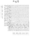
- Fig. 13 to 19 illustrate the arrangements of circuit patterns 7 on the circuit boards of the second to eighth layers.
- the land sequences for preferentially drawing the circuit patterns 7 are commonly set on each of the layers in order to preferentially draw the circuit patterns 7 in the same manner as that of the above-mentioned embodiments.
- the circuit patterns 7 are successively drawn starting from the first layer, and the lands 10 remaining on the circuit board are erased from the outer side but remain near the central portions. Thus, the lands 10 are gradually erased, and common electrodes for obtaining common potentials such as ground potential and power-source potential are formed in vacant space in the circuit board.
- the circuit patterns 7 are drawn from every land 10 on eight layers to cope with the normal lattice arrangement of 42 ⁇ 42 pin electrodes. Ten layers are required when this is done under the same conditions according to the prior art. Thus, the embodiment of the present invention makes it impossible to arrange the circuit patterns 7 on a multi-layer circuit board with a decreased number of layers.
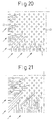
- circuit patterns 7 on a multi-layer circuit board for mounting an electronic part having electrodes arranged in a staggered lattice form, the total number of lands being 450 pins arranged under the following conditions.
- the distance between neighboring lands is a distance P between the closest lands (in a direction in parallel with a diagonal line) as shown in Fig. 23.
- the circuit pattern space is 223 ⁇ m between the lands of the of the outermost sequence, and two circuit patterns can be passed between these lands.
- circuit pattern space is 120 ⁇ m between the closest lands arranged in the direction of 45 degrees. Therefore, only one circuit pattern is allowed to be passed between the closest lands.
- the circuit patterns are drawn from the electrodes in the staggered lattice arrangement under the above-mentioned conditions, the same idea as that of the normal lattice arrangement can be applied.
- the circuit patterns are arranged by regarding the direction of a diagonal line tilted by 45 degrees relative to the direction of land arrangement of the outermost sequence to be the direction of land sequence for drawing the circuit patterns, so that the staggered lattice arrangement can be handled in the same manner as the normal lattice arrangement.
- Figs. 20 to 22 illustrate the arrangement of circuit patterns 7, according to the above-mentioned method, on each of the first to third layers.
- the land sequences in the direction of arrows are those from where the circuit patterns 7 are preferentially drawn.
- the lands 10 of every other sequences are erased.
- Figs. 20 to 22 illustrate the arrangement of circuit patterns 7 according to the method of preferentially drawing the circuit patterns from the same land sequence, and the circuit patterns 7 are drawn from every land 10 on three layers. Four or five layers will be required when the circuit patterns 7 are drawn starting from the outermost sequence successively into the inner side in the staggered lattice arrangement under the same conditions as shown in Fig. 23. According to the arrangement of this embodiment, on the other hand, it is possible to obtain a multi-layer circuit board while effectively decreasing the number of the circuit boards.
- the multi-layer circuit board has vias formed among the layers to electrically connect the circuit patterns among the layers.
- the vias formed among the layers may be formed vertically but the lands on an upper layer and the lands on a lower layer may often be formed slightly deviated in position on a plane.
- vias are vertically formed in the multi-layer circuit board, no limitation is imposed on the above-mentioned method.
- the lands on an upper layer and the lands on a lower layer are deviated in position on a plane, however, a limitation is often imposed on the arrangement of circuit patterns.
- the multi-layer circuit board of the present invention is for mounting an electronic part having electrodes arranged in a normal lattice form or in a staggered form, and is constituted by using circuit boards (wiring layers) in a number as small as possible, making it possible to improve the yield of production maintaining high reliability.
- the multi-layer circuit board of the present invention permits an increased number of circuit patterns (lands) to be drawn on each circuit board ccmpared with the prior art enabling vacant space to be formed on the circuit board and excellent electric properties to be provided by effectively utilizing the vacant space.
Landscapes
- Engineering & Computer Science (AREA)
- Microelectronics & Electronic Packaging (AREA)
- Manufacturing & Machinery (AREA)
- Production Of Multi-Layered Print Wiring Board (AREA)
- Wire Bonding (AREA)
Applications Claiming Priority (3)
| Application Number | Priority Date | Filing Date | Title |
|---|---|---|---|
| JP146993/97 | 1997-06-05 | ||
| JP14699397A JP3386977B2 (ja) | 1997-06-05 | 1997-06-05 | 多層回路基板 |
| JP14699397 | 1997-06-05 |
Publications (3)
| Publication Number | Publication Date |
|---|---|
| EP0883182A2 true EP0883182A2 (de) | 1998-12-09 |
| EP0883182A3 EP0883182A3 (de) | 1999-06-16 |
| EP0883182B1 EP0883182B1 (de) | 2005-09-21 |
Family
ID=15420187
Family Applications (1)
| Application Number | Title | Priority Date | Filing Date |
|---|---|---|---|
| EP98304446A Expired - Lifetime EP0883182B1 (de) | 1997-06-05 | 1998-06-04 | Gitteranordnung der Elektroden auf einer Mehrlagenleiterplatte |
Country Status (5)
| Country | Link |
|---|---|
| US (2) | US6229099B1 (de) |
| EP (1) | EP0883182B1 (de) |
| JP (1) | JP3386977B2 (de) |
| KR (1) | KR19990006616A (de) |
| DE (1) | DE69831629T2 (de) |
Cited By (13)
| Publication number | Priority date | Publication date | Assignee | Title |
|---|---|---|---|---|
| EP0928029A3 (de) * | 1997-12-22 | 1999-12-22 | Shinko Electric Industries Co. Ltd. | Mehrlagenschaltungs-Design |
| EP1085571A1 (de) * | 1999-09-20 | 2001-03-21 | Texas Instruments Incorporated | Verfahren zur Erhöhung der Zuverlässigkeit einer BGA-Verpackung |
| EP1087440A2 (de) * | 1999-09-22 | 2001-03-28 | Texas Instruments Incorporated | Modellierungstechnik zur Zuverlässigkeitserhöhung |
| EP1006577A3 (de) * | 1998-12-01 | 2001-05-16 | Shinko Electric Industries Co. Ltd. | Mehrlagenleiterplatte |
| EP1075026A3 (de) * | 1999-08-06 | 2001-12-19 | Shinko Electric Industries Co. Ltd. | Leiterplatten-Layout |
| WO2002093647A3 (en) * | 2001-05-15 | 2003-11-20 | Intel Corp | Electronic package with high density interconnect and associated methods |
| EP1460690A1 (de) * | 2003-02-25 | 2004-09-22 | Broadcom Corporation | Optimierung der Signalleitungen und des Platzbedarfs auf der Leiterplatte in einer Kugelmatrixverpackung |
| EP1071316B1 (de) * | 1999-07-22 | 2005-05-18 | Shinko Electric Industries Co., Ltd. | Mehrschichtige Leiterplatte |
| US6916995B2 (en) | 2003-02-25 | 2005-07-12 | Broadcom Corporation | Optimization of routing layers and board space requirements for ball grid array package implementations including single and multi-layer routing |
| DE10159444B4 (de) * | 2000-12-13 | 2008-04-10 | Lg. Philips Lcd Co., Ltd. | Flüssigkristallanzeige-Bildschirm und Verfahren zum Herstellen desselben |
| US7816247B2 (en) | 2003-02-25 | 2010-10-19 | Broadcom Corporation | Optimization of routing layers and board space requirements for ball grid array package implementations including array corner considerations |
| CN104103627A (zh) * | 2013-04-09 | 2014-10-15 | 瑞萨电子株式会社 | 半导体器件以及互连基板 |
| US9466578B2 (en) | 2013-12-20 | 2016-10-11 | Qualcomm Incorporated | Substrate comprising improved via pad placement in bump area |
Families Citing this family (21)
| Publication number | Priority date | Publication date | Assignee | Title |
|---|---|---|---|---|
| JP3825252B2 (ja) * | 2000-12-21 | 2006-09-27 | Necエレクトロニクス株式会社 | フリップチップ型半導体装置 |
| US8125087B2 (en) * | 2001-02-20 | 2012-02-28 | Intel Corporation | High-density flip-chip interconnect |
| WO2003065451A1 (en) * | 2002-01-31 | 2003-08-07 | Thomson Licensing S.A. | Flip chip die bond pads, die bond pad placement and routing optimization |
| JP3815342B2 (ja) * | 2002-02-19 | 2006-08-30 | 株式会社デンソー | 半導体装置 |
| US6875930B2 (en) * | 2002-04-18 | 2005-04-05 | Hewlett-Packard Development Company, L.P. | Optimized conductor routing for multiple components on a printed circuit board |
| KR100693669B1 (ko) * | 2003-03-03 | 2007-03-09 | 엘지전자 주식회사 | 피일드 매크로 블록의 레퍼런스 픽쳐 결정 방법 |
| US7345245B2 (en) * | 2003-10-08 | 2008-03-18 | Lsi Logic Corporation | Robust high density substrate design for thermal cycling reliability |
| JP4429760B2 (ja) * | 2004-02-20 | 2010-03-10 | 新光電気工業株式会社 | 多層配線基板 |
| GB2414864A (en) * | 2004-06-01 | 2005-12-07 | Nokia Corp | Detecting short circuits |
| JP4086816B2 (ja) | 2004-07-01 | 2008-05-14 | 株式会社Nec情報システムズ | Bga部品搭載基板の層数見積もり装置及び方法並びに層数見積もりプログラム |
| FR2879813A1 (fr) * | 2004-12-17 | 2006-06-23 | St Microelectronics Sa | Dispositif de connexion electrique d'une puce de circuits integres sur une plaque principale |
| US20060185895A1 (en) * | 2005-02-24 | 2006-08-24 | Navinchandra Kalidas | Universal pattern of contact pads for semiconductor reflow interconnections |
| US7928549B2 (en) * | 2006-09-19 | 2011-04-19 | Taiwan Semiconductor Manufacturing Co., Ltd. | Integrated circuit devices with multi-dimensional pad structures |
| EP1978560A1 (de) * | 2007-04-04 | 2008-10-08 | Stmicroelectronics SA | Leiterplatte, deren Herstellung und Herstllung eines Halbleiterbauteils mit einem Chip mit integrierter Schaltung |
| US7816610B2 (en) * | 2007-04-19 | 2010-10-19 | Mediatek Inc. | Layout circuit |
| US8053349B2 (en) * | 2007-11-01 | 2011-11-08 | Texas Instruments Incorporated | BGA package with traces for plating pads under the chip |
| DE102009010055A1 (de) | 2008-03-11 | 2009-10-01 | Merkel, Tobias, Dr. | Virtuelles Mikrofon mit fremdmoduliertem Ultraschall |
| US9633965B2 (en) | 2014-08-08 | 2017-04-25 | Taiwan Semiconductor Manufacturing Company Ltd. | Semiconductor structure and manufacturing method of the same |
| US9749723B2 (en) * | 2015-03-05 | 2017-08-29 | Huawei Technologies Co., Ltd. | System and method for optical network |
| JP7279624B2 (ja) | 2019-11-27 | 2023-05-23 | 株式会社ソシオネクスト | 半導体装置 |
| CN118923213A (zh) | 2022-03-31 | 2024-11-08 | 京瓷株式会社 | 布线基板以及安装构造体 |
Family Cites Families (4)
| Publication number | Priority date | Publication date | Assignee | Title |
|---|---|---|---|---|
| JPS5890747A (ja) * | 1981-11-25 | 1983-05-30 | Nec Corp | Lsiパツケ−ジ |
| US4782193A (en) * | 1987-09-25 | 1988-11-01 | Ibm Corp. | Polygonal wiring for improved package performance |
| US5467252A (en) * | 1993-10-18 | 1995-11-14 | Motorola, Inc. | Method for plating using nested plating buses and semiconductor device having the same |
| US5557505A (en) * | 1994-07-22 | 1996-09-17 | Ast Research, Inc. | Dual pattern microprocessor package footprint |
-
1997
- 1997-06-05 JP JP14699397A patent/JP3386977B2/ja not_active Expired - Fee Related
-
1998
- 1998-06-03 KR KR1019980020504A patent/KR19990006616A/ko not_active Withdrawn
- 1998-06-04 EP EP98304446A patent/EP0883182B1/de not_active Expired - Lifetime
- 1998-06-04 DE DE69831629T patent/DE69831629T2/de not_active Expired - Fee Related
- 1998-06-05 US US09/092,845 patent/US6229099B1/en not_active Expired - Fee Related
-
2001
- 2001-02-13 US US09/781,302 patent/US6452115B2/en not_active Expired - Fee Related
Cited By (24)
| Publication number | Priority date | Publication date | Assignee | Title |
|---|---|---|---|---|
| EP0928029A3 (de) * | 1997-12-22 | 1999-12-22 | Shinko Electric Industries Co. Ltd. | Mehrlagenschaltungs-Design |
| US6335493B1 (en) | 1998-12-01 | 2002-01-01 | Shinko Electric Industries, Co., Ltd. | Multilayer wiring board |
| EP1006577A3 (de) * | 1998-12-01 | 2001-05-16 | Shinko Electric Industries Co. Ltd. | Mehrlagenleiterplatte |
| EP1071316B1 (de) * | 1999-07-22 | 2005-05-18 | Shinko Electric Industries Co., Ltd. | Mehrschichtige Leiterplatte |
| US6407344B1 (en) | 1999-08-06 | 2002-06-18 | Shinko Electric Industries Co., Ltd | Multilayer circuit board |
| EP1075026A3 (de) * | 1999-08-06 | 2001-12-19 | Shinko Electric Industries Co. Ltd. | Leiterplatten-Layout |
| EP1085571A1 (de) * | 1999-09-20 | 2001-03-21 | Texas Instruments Incorporated | Verfahren zur Erhöhung der Zuverlässigkeit einer BGA-Verpackung |
| EP1087440A2 (de) * | 1999-09-22 | 2001-03-28 | Texas Instruments Incorporated | Modellierungstechnik zur Zuverlässigkeitserhöhung |
| DE10159444B4 (de) * | 2000-12-13 | 2008-04-10 | Lg. Philips Lcd Co., Ltd. | Flüssigkristallanzeige-Bildschirm und Verfahren zum Herstellen desselben |
| DE10159444B9 (de) * | 2000-12-13 | 2008-09-25 | Lg. Philips Lcd Co., Ltd. | Flüssigkristallanzeige-Bildschirm und Verfahren zum Herstellen desselben |
| US7414692B2 (en) | 2000-12-13 | 2008-08-19 | Lg Display Co., Ltd. | Liquid crystal display panel comprising data lines having alternately different extended lengths to data pads at respectively different levels above the substrate |
| WO2002093647A3 (en) * | 2001-05-15 | 2003-11-20 | Intel Corp | Electronic package with high density interconnect and associated methods |
| US6664483B2 (en) | 2001-05-15 | 2003-12-16 | Intel Corporation | Electronic package with high density interconnect and associated methods |
| CN1526166B (zh) * | 2001-05-15 | 2010-05-26 | 英特尔公司 | 具有高密度互连的电子封装件和相关方法 |
| US7005753B2 (en) | 2003-02-25 | 2006-02-28 | Broadcom Corporation | Optimization of routing layers and board space requirements for a ball grid array land pattern |
| US7009115B2 (en) | 2003-02-25 | 2006-03-07 | Broadcom Corporation | Optimization of routing layers and board space requirements for a ball grid array package |
| US6916995B2 (en) | 2003-02-25 | 2005-07-12 | Broadcom Corporation | Optimization of routing layers and board space requirements for ball grid array package implementations including single and multi-layer routing |
| EP1460690A1 (de) * | 2003-02-25 | 2004-09-22 | Broadcom Corporation | Optimierung der Signalleitungen und des Platzbedarfs auf der Leiterplatte in einer Kugelmatrixverpackung |
| US7816247B2 (en) | 2003-02-25 | 2010-10-19 | Broadcom Corporation | Optimization of routing layers and board space requirements for ball grid array package implementations including array corner considerations |
| US7855448B2 (en) | 2003-02-25 | 2010-12-21 | Broadcom Corporation | Optimization of routing layers and board space requirements for ball grid array package implementations including array corner considerations |
| US8695212B2 (en) | 2003-02-25 | 2014-04-15 | Broad Corporation | Method for optimizing routing layers and board space requirements for a ball grid array land pattern |
| CN104103627A (zh) * | 2013-04-09 | 2014-10-15 | 瑞萨电子株式会社 | 半导体器件以及互连基板 |
| CN104103627B (zh) * | 2013-04-09 | 2018-04-10 | 瑞萨电子株式会社 | 半导体器件以及互连基板 |
| US9466578B2 (en) | 2013-12-20 | 2016-10-11 | Qualcomm Incorporated | Substrate comprising improved via pad placement in bump area |
Also Published As
| Publication number | Publication date |
|---|---|
| EP0883182A3 (de) | 1999-06-16 |
| US6229099B1 (en) | 2001-05-08 |
| DE69831629D1 (de) | 2006-02-02 |
| JPH10335532A (ja) | 1998-12-18 |
| US20010009203A1 (en) | 2001-07-26 |
| EP0883182B1 (de) | 2005-09-21 |
| DE69831629T2 (de) | 2006-03-16 |
| JP3386977B2 (ja) | 2003-03-17 |
| KR19990006616A (ko) | 1999-01-25 |
| US6452115B2 (en) | 2002-09-17 |
Similar Documents
| Publication | Publication Date | Title |
|---|---|---|
| EP0883182A2 (de) | Gitteranordnung der Elektroden auf einer Mehrlagenleiterplatte | |
| US6271478B1 (en) | Multi-layer circuit board | |
| US6194668B1 (en) | Multi-layer circuit board | |
| US8054643B2 (en) | Semiconductor module, wiring board, and wiring method | |
| US5357140A (en) | Semiconductor device capable of laminating a plurality of wiring layers which are more than four layers | |
| US6335493B1 (en) | Multilayer wiring board | |
| US6407343B1 (en) | Multilayer wiring board | |
| EP1075026A2 (de) | Leiterplatten-Layout | |
| JP3610262B2 (ja) | 多層回路基板及び半導体装置 | |
| US7394026B2 (en) | Multilayer wiring board | |
| JP3462385B2 (ja) | 多層回路基板 | |
| US8013253B2 (en) | Electrical connection board and assembly of such a board and a semiconductor component comprising an integrated circuit chip | |
| JPH1140698A (ja) | 配線基板 | |
| HK1018541A (en) | Multi-layer circuit board layout | |
| JP4397628B2 (ja) | 印刷回路配線板の配線レイアウト構造 | |
| HK1029009A (en) | Multilayer wiring board |
Legal Events
| Date | Code | Title | Description |
|---|---|---|---|
| PUAI | Public reference made under article 153(3) epc to a published international application that has entered the european phase |
Free format text: ORIGINAL CODE: 0009012 |
|
| AK | Designated contracting states |
Kind code of ref document: A2 Designated state(s): DE FR GB |
|
| AX | Request for extension of the european patent |
Free format text: AL;LT;LV;MK;RO;SI |
|
| PUAL | Search report despatched |
Free format text: ORIGINAL CODE: 0009013 |
|
| AK | Designated contracting states |
Kind code of ref document: A3 Designated state(s): AT BE CH CY DE DK ES FI FR GB GR IE IT LI LU MC NL PT SE |
|
| AX | Request for extension of the european patent |
Free format text: AL;LT;LV;MK;RO;SI |
|
| 17P | Request for examination filed |
Effective date: 19991115 |
|
| AKX | Designation fees paid |
Free format text: DE FR GB |
|
| 17Q | First examination report despatched |
Effective date: 20040429 |
|
| GRAP | Despatch of communication of intention to grant a patent |
Free format text: ORIGINAL CODE: EPIDOSNIGR1 |
|
| GRAS | Grant fee paid |
Free format text: ORIGINAL CODE: EPIDOSNIGR3 |
|
| GRAA | (expected) grant |
Free format text: ORIGINAL CODE: 0009210 |
|
| AK | Designated contracting states |
Kind code of ref document: B1 Designated state(s): DE FR GB |
|
| REG | Reference to a national code |
Ref country code: GB Ref legal event code: FG4D |
|
| REF | Corresponds to: |
Ref document number: 69831629 Country of ref document: DE Date of ref document: 20051027 Kind code of ref document: P |
|
| REF | Corresponds to: |
Ref document number: 69831629 Country of ref document: DE Date of ref document: 20060202 Kind code of ref document: P |
|
| PG25 | Lapsed in a contracting state [announced via postgrant information from national office to epo] |
Ref country code: GB Free format text: LAPSE BECAUSE OF NON-PAYMENT OF DUE FEES Effective date: 20060604 |
|
| ET | Fr: translation filed | ||
| PLBE | No opposition filed within time limit |
Free format text: ORIGINAL CODE: 0009261 |
|
| STAA | Information on the status of an ep patent application or granted ep patent |
Free format text: STATUS: NO OPPOSITION FILED WITHIN TIME LIMIT |
|
| 26N | No opposition filed |
Effective date: 20060622 |
|
| PG25 | Lapsed in a contracting state [announced via postgrant information from national office to epo] |
Ref country code: DE Free format text: LAPSE BECAUSE OF NON-PAYMENT OF DUE FEES Effective date: 20070103 |
|
| GBPC | Gb: european patent ceased through non-payment of renewal fee |
Effective date: 20060604 |
|
| REG | Reference to a national code |
Ref country code: FR Ref legal event code: ST Effective date: 20070228 |
|
| PG25 | Lapsed in a contracting state [announced via postgrant information from national office to epo] |
Ref country code: FR Free format text: LAPSE BECAUSE OF NON-PAYMENT OF DUE FEES Effective date: 20060630 |