EP0883250B1 - Emetteur de communications mobiles avec des amplificateurs sélectivement activés - Google Patents
Emetteur de communications mobiles avec des amplificateurs sélectivement activés Download PDFInfo
- Publication number
- EP0883250B1 EP0883250B1 EP98110485A EP98110485A EP0883250B1 EP 0883250 B1 EP0883250 B1 EP 0883250B1 EP 98110485 A EP98110485 A EP 98110485A EP 98110485 A EP98110485 A EP 98110485A EP 0883250 B1 EP0883250 B1 EP 0883250B1
- Authority
- EP
- European Patent Office
- Prior art keywords
- amplifier
- output
- control circuit
- amplifiers
- circuit
- Prior art date
- Legal status (The legal status is an assumption and is not a legal conclusion. Google has not performed a legal analysis and makes no representation as to the accuracy of the status listed.)
- Expired - Lifetime
Links
- 230000003213 activating effect Effects 0.000 title claims 2
- 238000010295 mobile communication Methods 0.000 title description 10
- 230000005540 biological transmission Effects 0.000 claims description 73
- 238000001514 detection method Methods 0.000 claims description 11
- 238000010586 diagram Methods 0.000 description 7
- 230000009977 dual effect Effects 0.000 description 7
- 238000012937 correction Methods 0.000 description 6
- 238000000034 method Methods 0.000 description 6
- 230000001105 regulatory effect Effects 0.000 description 5
- 230000008859 change Effects 0.000 description 4
- 230000003321 amplification Effects 0.000 description 3
- 230000001419 dependent effect Effects 0.000 description 3
- 238000003199 nucleic acid amplification method Methods 0.000 description 3
- 238000013459 approach Methods 0.000 description 2
- 230000006870 function Effects 0.000 description 2
- 238000004519 manufacturing process Methods 0.000 description 2
- 230000004044 response Effects 0.000 description 2
- 230000008054 signal transmission Effects 0.000 description 2
- 230000001174 ascending effect Effects 0.000 description 1
- 230000008901 benefit Effects 0.000 description 1
- 230000001413 cellular effect Effects 0.000 description 1
- 238000004891 communication Methods 0.000 description 1
- 230000001276 controlling effect Effects 0.000 description 1
- 230000008878 coupling Effects 0.000 description 1
- 238000010168 coupling process Methods 0.000 description 1
- 238000005859 coupling reaction Methods 0.000 description 1
- 238000013461 design Methods 0.000 description 1
- 230000005669 field effect Effects 0.000 description 1
- 230000006872 improvement Effects 0.000 description 1
- 238000003780 insertion Methods 0.000 description 1
- 230000037431 insertion Effects 0.000 description 1
Images




Classifications
-
- H—ELECTRICITY
- H03—ELECTRONIC CIRCUITRY
- H03F—AMPLIFIERS
- H03F1/00—Details of amplifiers with only discharge tubes, only semiconductor devices or only unspecified devices as amplifying elements
- H03F1/02—Modifications of amplifiers to raise the efficiency, e.g. gliding Class A stages, use of an auxiliary oscillation
- H03F1/0205—Modifications of amplifiers to raise the efficiency, e.g. gliding Class A stages, use of an auxiliary oscillation in transistor amplifiers
- H03F1/0277—Selecting one or more amplifiers from a plurality of amplifiers
-
- H—ELECTRICITY
- H03—ELECTRONIC CIRCUITRY
- H03F—AMPLIFIERS
- H03F3/00—Amplifiers with only discharge tubes or only semiconductor devices as amplifying elements
- H03F3/72—Gated amplifiers, i.e. amplifiers which are rendered operative or inoperative by means of a control signal
-
- H—ELECTRICITY
- H03—ELECTRONIC CIRCUITRY
- H03G—CONTROL OF AMPLIFICATION
- H03G1/00—Details of arrangements for controlling amplification
- H03G1/0005—Circuits characterised by the type of controlling devices operated by a controlling current or voltage signal
- H03G1/0088—Circuits characterised by the type of controlling devices operated by a controlling current or voltage signal using discontinuously variable devices, e.g. switch-operated
-
- H—ELECTRICITY
- H03—ELECTRONIC CIRCUITRY
- H03G—CONTROL OF AMPLIFICATION
- H03G3/00—Gain control in amplifiers or frequency changers
- H03G3/20—Automatic control
- H03G3/30—Automatic control in amplifiers having semiconductor devices
- H03G3/3036—Automatic control in amplifiers having semiconductor devices in high-frequency amplifiers or in frequency-changers
- H03G3/3042—Automatic control in amplifiers having semiconductor devices in high-frequency amplifiers or in frequency-changers in modulators, frequency-changers, transmitters or power amplifiers
-
- H—ELECTRICITY
- H03—ELECTRONIC CIRCUITRY
- H03F—AMPLIFIERS
- H03F2203/00—Indexing scheme relating to amplifiers with only discharge tubes or only semiconductor devices as amplifying elements covered by H03F3/00
- H03F2203/72—Indexing scheme relating to gated amplifiers, i.e. amplifiers which are rendered operative or inoperative by means of a control signal
- H03F2203/7239—Indexing scheme relating to gated amplifiers, i.e. amplifiers which are rendered operative or inoperative by means of a control signal the gated amplifier being switched on or off by putting into parallel or not, by choosing between amplifiers and shunting lines by one or more switch(es)
-
- H—ELECTRICITY
- H04—ELECTRIC COMMUNICATION TECHNIQUE
- H04B—TRANSMISSION
- H04B1/00—Details of transmission systems, not covered by a single one of groups H04B3/00 - H04B13/00; Details of transmission systems not characterised by the medium used for transmission
- H04B1/02—Transmitters
- H04B1/04—Circuits
- H04B2001/0408—Circuits with power amplifiers
- H04B2001/0416—Circuits with power amplifiers having gain or transmission power control
Definitions
- the present invention relates to a mobile communication transmitter mounted on a mobile station for communicating with a base station.
- amplifiers constituting a transmission power amplifying section take most of the power dissipated in the telephone set and hence the performance of the portable telephone set in terms of sustainable duration of call is heavily dependent on the efficiency of signal transmission of the transmission power amplifying section.
- the efficiency of signal transmission of the transmission power amplifying section of the portable telephone set is expressed by the ratio of high frequency output power/input DC power.
- the efficiency is determined by the impedance characteristics of the matching circuits of the amplifiers. However, since the impedance characteristics of the matching circuits vary depending on the output power and the transmitter frequency, the impedance of the matching circuits has to be selected according to the transmitter frequency and the output power to be used for the portable telephone set.
- the matching circuits of the amplifiers have a fixed impedance that is selected to realize a maximum efficiency for a maximum power output in the frequency band to be used with the portable telephone set in order to amplify a high frequency wave highly efficiently. This will be explained later in detail.
- the transmission power amplifying section of the transmitter is accompanied by the problem of a reduced efficiency at a low output level.
- JP-A-57-60739 discloses a transmitter adapted to automatically select an output matching circuit that can minimize the efficiency out of a plurality of prearranged output matching circuits in order to improve the efficiency for low output operation.
- This transmitter is formed by a controller for issuing a switch signal for selecting an output matching circuit and an optimal value determining unit for selecting an optimal matching circuit and transmitting a signal to a matching switch circuit in addition to the components of the conventional portable telephone system.
- the amplifiers (transistors) of the transmitter are not modified if an optimal output matching circuit is selected as a function of the output power level. In other words, no improvement can be expected for the efficiency of the transmitter in the operating zone of 10 to 30dB below the maximum output level if it is used for a portable telephone set.
- the transistors show a fall in the efficiency of amplification when they are driven in the operating zone of 10 to 30dB below the maximum output level if compared with transistors having an optimal size. The reasons for this are as follows:
- the efficiency of operation of the transistors having a size optimally adapted to a low output level is by far higher than the efficiency of operation of the transistors having a larger size particularly in the operating zone around the maximum output level.
- the ratio of the maximum transmission output and the minimum transmission output is referred to as output dynamic range, which is about 30dB for conventional portable telephone sets.
- output dynamic range is about 30dB for conventional portable telephone sets.
- an output dynamic range of 60 to 70 dB is required for portable telephone sets to be used for a code division multiple access (CDMA) system that has become commercially available recently.
- CDMA code division multiple access
- JP-A-57-60739 With the transmitter of JP-A-57-60739, the transistor arranged in the last stage has a predetermined size and hence shows an efficiency of less than 10% for a low output level of about +10 to -10dBm as in the case of the above described amplifiers if an optimal output matching circuit is selected out of a plurality of matching circuits as a function of the output level.
- the technique disclosed in JP-A-57-60739 is not effective for achieving a wide output range. It should be noted here that JP-A-57-60739 describes only a transmitter with 0.5W (+27dBm) for a low output level and 2W (+33dBm) for the maximum output level as a specific example.
- a transmitter as described in JP-A-57-60739 is constructed by PIN diodes as means for selecting an output matching circuit, which has to be constantly biased so that all the output matching circuits may be switched sequentially. Then, an electric current of several mA flows through the biased PIN diodes. Since a pair of PIN diodes are required for each of the output matching circuits, a total of 2 x n PIN diodes have to be used for "n" matching circuits. If a PIN diode consumes power at a rate of 1mA, then the power dissipation of all the PIN diodes will be n ⁇ 2mA regardless of the output power of the transmitter. This raises a serious problem for a portable telephone set that is required to be of power saving type.
- WO 96/36105 discloses a high efficiency multiple power level amplifier circuit for reducing power consumption during lower power operations.
- a plurality of power amplifiers stages are cascaded to provided multiple levels of amplification.
- At least one power amplification stage includes a signal switching network to allow one or any combination of power amplifiers to be switched out when lower power operations are desired.
- the switched out power amplifiers are biased such that substantially no current is drawn from the power source.
- Claim 2 defines a particular embodiment of the invention.
- a transmission power amplifying section is formed by a plurality of amplifiers, and a plurality of switch circuits are connected to the outputs of the amplifiers, respectively.
- a control circuit is connected to the amplifiers and the switch circuits, and activates at least one of the amplifiers and operates the switch circuits to serially connect the at least one amplifier in accordance with the distance between the mobile station and the base station.
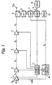
- Fig. 1 which illustrates a prior art mobile communication transmitter mounted in a mobile station
- an input signal S in is amplified by an automatic gain control (AGC) amplifier 1 and amplifiers 2, 3 and 4, and is output via a directional coupler 5 as an output signal S out .
- AGC automatic gain control
- the AGC amplifier 1 amplifies the input signal S in with an AGC gain determined by an AGC control voltage, and generates an output signal S 1 .
- the amplifier 2 amplifies the output signal S 1 of the AGC amplifier 1 with a constant gain and generates an output signal S 2 .
- the amplifier 3 amplifies the output signal S 2 of the amplifier 2 with a constant gain and generates an output signal S 3 .
- the amplifier 4 amplifies the output signal S 3 of the amplifier 3 with a constant gain and generates an output signal S 4 .
- the directional coupler 5 generates about 1/100 of the output signal S 4 of the amplifier 4 to a detector 6 and generates the remaining output as the output signal S out .
- the detector 6 detects the output signal from the directional coupler 5 and outputs it as a detection voltage V D .
- a comparator 7 compares the detection voltage V D from the detector 6 with a reference voltage V R from a control circuit 9, and generates a correction signal S 5 and transmits it to an AGC voltage control circuit 7a to compensate for the difference between the detection voltage V D and the reference voltage V R .
- the AGC voltage control circuit 7a generates the AGC control voltage in accordance with the correction signal S 5 .
- the mobile station system is typically provided with a functional feature of automatic power control (APC) for controlling the output power of the transmitter by selecting one of several predetermined power levels according to the distance between a base station and the mobile station.
- APC automatic power control
- the mobile station detects the signal strength of radio waves transmitted from the base station and received by it by means of a received signal strength indicator (RSSI) 8 in order to obtain a signal S 6 on the distance between the base station and the mobile station.
- RSSI received signal strength indicator
- the distance signal S 6 is then transmitted to a control circuit 9.
- the control circuit 9 reads out the reference voltage V R from a read-only memory (ROM) 10 using the distance signal S 6 as an argument.
- the control circuit 9 also controls a power supply source 11 for supplying power supply voltage to the AGC amplifier 1, the amplifiers 2, 3 and 4, and the AGC voltage control circuit 7a in accordance with the system requirement. For example, the control circuit 9 periodically turns OFF the power supply source 11, thus reducing the power dissipation.
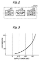
- the amplifier 2 is formed by an input matching circuit 201 with a fixed impedance, an amplifying section 202 typically constituted by a field effect transistor (FET) and an output matching circuit 203 with a fixed impedance.
- the amplifier 2 is made to match the characteristic impedance of 50 ⁇ by the input matching circuit 201 and the output matching circuit 203 in order to realize a maximum efficiency within a range selected to satisfy the required distortion characteristics.
- the amplifiers 3 and 4 have the same configuration as the amplifier 2.
- the input matching circuit 201 and the output matching circuits 203 of the amplifiers 2, 3 and 4 are so arranged as to realize a maximum efficiency when the output power of the amplifier 4 reaches its maximum level.
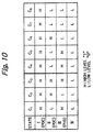
- the matching circuits 201 and 203 are so arranged as to realize a maximum efficiency for the amplifying sections when the output of the APC reaches its maximum level, the efficiency of the transmission power amplifying section (2, 3, 4) will be reduced when the output power level is lowered, as shown in Fig. 3.
- the transmission power amplifying section (2, 3, 4) shows an efficiency of 60% or more with an output level of 1W ( + 30 dBm) or higher, but the efficiency falls below 10% when the output level is reduced by 20dB (to + 10dBm).
- a difference between the maximum output level and the minimum output level of the APC is about 20 to 30dB, and the APC is operating with the minumum output level in urban areas and in areas where the mobile station is located close to the base station.
- the mobile station shows a low efficiency for the transmission power amplifying section (2, 3, 4) when the output power level is low, it cannot effectively reduce the power dissipation if it is used in such areas.
- a switch circuit 21 is provided between the amplifiers 2 and 3 of Fig. 1
- a switch circuit 22 is provided between the amplifiers 3 and 4 of Fig. 1
- a switch circuit 23 is provided between the amplifier 4 and the directional coupler 5 of Fig. 1.
- the switch circuits 21, 22 and 23 are connected in series.
- a bias control circuit 24 is provided between the power supply source 11 and the amplifier 3 of Fig. 1
- a bias control circuit 25 is provided between the power supply source 11 and the amplifier 4 of Fig. 1.
- a voltage control circuit 26 controls the switch circuits 21, 22 and 23 and the bias control circuits 24 and 25.
- a control circuit 9' is provided instead of the control circuit 9 of Fig. 1.
- the control circuit 9' controls the voltage control circuit 26 in addition to the comparator 7 and the power supply source 11. That is, the control circuit 9' reads out the reference voltage V R from the ROM 10 using the distance signal S 6 as an argument. Also, the control circuit 9' reads out control signals C 1 , C 2 and C 3 from the ROM 10 using the distance signal S 6 as an argument.
- the voltage control circuit 26 receives the control signals C 1 and C 2 from the control circuit 9' to generate control signals C 4 , C 5 , C 6 , C 7 and C 8 .
- the voltage control circuit 26 is illustrated in Fig. 5.
- control circuit 9' generates the control signals C 1 , C 2 and C 3 as shown in Fig. 6, the voltage control circuit 26 generates the control signals C 4 , C 5 , C 6 , C 7 and C 8 as shown in Fig. 6.
- control signal C 3 is an OR logic between the control signals C 1 and C 2 .
- SPDT single pole dual throw
- DPDT double pole dual throw
- the switch circuits 21, 22 and 23 are preferably terminating type switches in order to minimize the return loss that arises when turned OFF.
- the amplifiers 2, 3, and 4 have different element sizes and are arranged in the ascending order of their output power levels or in the order of the amplifier 2, the amplifier 3 and the amplifier 4 in order to realize a high efficiency.
- the switch circuits 21, 22 and 23 and the amplifiers 2, 3 and 4 are controlled for switching states I , II and III as shown in Fig. 6 in such a way that the output power level to be selected for each element is predetermined in order to realize a high efficiency over a wide dynamic range and the data relating to the switching operation of each element are stored in the ROM 10.
- the APC operation that does not need to change the number of the amplifiers 2, 3 and 4 is conducted by modifying the gain of the AGC amplifier 1 by means of the AGC voltage control circuit 7a as in the transmitter of Fig. 1.
- the switching control of the states I , II and III has priority over the APC so that an APC operation can take place only after the switching control.
- the states I , II and III of Fig. 6 are dependent upon the distance between the mobile station and the base station, i.e., the distance signal S 6 .
- a signal to be transmitted is firstly modulated by a base band section (not shown) and then made to show the transmission frequency before it is entered into the AGC amplifier 1.
- the control information read out of the ROM 10 in correspondence to the distance signal S 6 serves to adapt the transmission power amplifying section to the maximum output level.
- the control circuit 9' generates a reference voltage V R to the comparator 7 that makes the transmission power amplifying section adapt to the maximum output level.
- the control circuit 9' causes the control signals C 1 , C 2 and C 3 to be high (see state I of Fig. 6) in order to adapt the transmission power amplifying section to the maximum output level.
- the power supply source 11 is turned ON by the control signal C 3 so that consequently the AGC voltage control circuit 7a, the AGC amplifier 1, the amplifier 2, and the bias control circuits 24 and 25 are fed with a power supply voltage.
- the bias control circuit 24 forwards the voltage from the power supply source 11 to the amplifier 3, while the bias control circuit 25 forwards the voltage from the power supply source 11 to the amplifier 4.
- the amplifiers 2, 3 and 4 are activated.
- the switch circuit 21 forwards the output of the amplifier 2 to the amplifier 3, and the switch circuit 22 forwards the output of the amplifier 3 to the amplifier 4, and the switch circuit 23 forwards the output of the amplifier 4 to the directional coupler 5.
- the transmission signal entered into the AGC amplifier 1 is output by way of the route of the amplifier 2 ⁇ the switch circuit 21 ⁇ the amplifier 3 ⁇ the switch circuit 22 ⁇ the amplifier 4 ⁇ the switch circuit 23 ⁇ the directional coupler 5.
- the directional coupler 5 transmits a signal with a level of a hundredth of the transmission output level to the detector 6.
- the output of the directional coupler 5 is transformed into a detection voltage V D that is a DC voltage detected by the detector 6 and then sent to the comparator 7.
- the comparator 7 compares the detection voltage V D with the reference voltage V R from the control circuit 9' so that a correction signal S 5 is transmitted to the AGC voltage control circuit 7a in order to minimize the difference between the detection voltage V D and the reference voltage V R .
- the AGC voltage control circuit 7a regulates the gain of the AGC amplifier 1 by modifying the AGC voltage to shift the output power level to the amplifier 2 to the level specified by the correction signal S 5 . In this way, the control circuit 9' sets the output power level of the output terminal of the switch circuit 23 to a desired value.
- Curve I in Fig. 8 shows the relationship between the output power of the transmission power amplifying section and the efficiency of its operation in state I as shown in Fig. 7A. Note that, if the maximum output level of the mobile station is +31dBm, the efficiency of the transmission power amplifying section will be about 60%.
- the AGC amplifier 1 is regulated to reduce its gain and hence the output level of the transmission power amplifying section is lowered in response to the change in the distance signal S 6 .
- the efficiency of the transmission power amplifying section is reduced from the maximum output level. For example, if the efficiency of the outpuft power of +31dBm is 60%, it will be lowered to somewhere around 20% when the output power is reduced to +20dBm.
- the amplifier 3 is connected via the switch circuits 22 and 23 to the directional coupler 5.
- the bias control circuit 25 interrupts the supply of voltage to the amplifier 4, so that the amplifier 4 is deactivated, thus reducing the power dissipation. Consequently, as shown in Fig.
- the transmission signal entered into the AGC amplifier 1 is output by way of the route of the amplifier 2 ⁇ the switch circuit 21 ⁇ the amplifier 3 ⁇ the switch circuit 22 ⁇ the switch circuit 23 - ⁇ the directional coupler 5.
- the amplifiers 2 and 3 are turned ON while the amplifier 4 is turned OFF.
- Curve II in Fig. 8 shows the relationship between the output power of the transmission power amplifying section and the efficiency of its operation under state II as shown in Fig. 6. It will be seen from Fig. 8 that the transmission power amplifying section shows an efficiency of about 60% when the output power is about +23dBm to +24dBm.
- the gain of the AGC amplifier 1 is regulated to reduce the output power of the transmission power amplifying section to lower the efficiency of operation of the transmission power amplifying section. For example, the efficiency will become as low as 20 % when the output power at the output terminal of the switch circuit 23 is reduced to about +12dBm.
- the amplifier 2 is connected via the switch circuits 21, 22 and 23 to the directional coupler 5. Simultaneously, the bias circuit 24 interrupts the supply of voltage to the amplifier 3, so that the amplifier 3 is deactivated, thus reducing the power dissipation.
- the transmission signal entered into the AGC amplifier 1 is output by way of the route of the amplifier 2 ⁇ the switch circuit 21 ⁇ the switch circuit 22 ⁇ the switch circuit 23 ⁇ the directional coupler 5.
- the amplifier 2 is turned ON while the amplifiers 3 and 4 are turned OFF so that the output of the amplifier 2 is directly used as output power of the transmission power amplifying section of the mobile station.
- Curve III in Fig. 8 shows the relationship between the output power of the transmission power amplifying section and the efficiency of its operation under state III as shown in Fig. 6. It will be seen from Fig. 8 that the transmission power amplifying section shows an efficiency slightly lower than 60% when the output power is reduced to about +12dBm to 13dBm.
- the AGC voltage control circuit 7a, and the AGC circuit 1 are deactivated.
- Fig. 7D all the amplifiers 2, 3 and 4 are deactivated.
- the transmission power amplifying section operates with an efficiency of about 60% over a wide output power range between +12dBm and +31dBm.
- the efficiency of the transmission power amplifying section can be held to a high level over a wide output dynamic range.
- a general sequential control technique may be used for the first embodiment if the elements employed in the amplifiers 2 through 4 require special consideration in the manner of biasing or, for example, a gate bias voltage and a drain bias voltage have to be sequentially applied in the above order for biasing the FETs of the amplifiers.
- the first embodiment can be used for a portable telephone system or the like without modifying any other elements of the system.
- variable range of the gain of the AGC amplifier 1 can be reduced by more than 20dB because the transmission power is regulated by selectively using the amplifiers 2, 3 and 4.
- amplifiers 2, 3 and 4 are matched to provide a maximum efficiency for the maximum output level in the first embodiment, it is a known practice in the design of amplifiers to arrange matching circuits so as to achieve a maximum efficiency under the conditions that satisfy desired distortion characteristics if they are used in a system that requires the adjacent channel leakage power to be suppressed below a specified level.
- CDMA code division multiple access
- a dual band system is adopted. That is, an SPDT type switch circuit 31 formed by an SPDT switch circuit is provided instead of the DPDT type switch circuit 22 of Fig. 4, and a matching circuit 32 and a directional coupler 33 for generating an output signal S out ' are connected to the switch circuit 31.
- the matching circuit 32 makes the output of the switch circuit 31 match the selected impedance and forwards this output to the directional coupler 33.
- a desired frequency band can be selected for the maximum efficiency.
- the directional coupler 33 has the same configuration as the directional coupler 5 and is arranged at the output side of the matching circuit 32 so that a transmission output with a power level that is about a hundredth of the power level of the output generated by way of the matching circuit 32 is fed to the detector 6.
- the second embodiment is applied to the transmission power amplifying section of a mobile station adapted to both a personal digital cellular (PDC) system which is a digital portable telephone system available in Japan and a personal handy-phone (PHS) system which is a digital cordless system also available in Japan.
- the amplifiers of the mobile station are required to match these different frequencies optimally.
- the maximum output level is about +30.5dBm for the PDC system and about +21dBm for the PHS system.
- the amplifiers 2 and 3 will be designed as wide band amplifiers having an operating frequency between 900MHz and 1.9GHz and the respective input matching circuit of the amplifiers 2 and 3 (see Fig. 2) will be designed to operate in a desired manner between 925MHz and 1,920MHz.
- the amplifiers 2, 3 and 4 of the second embodiment have the same configuration as those of Fig. 4.
- the amplifier 4 is adapted to be matched so as to provide a maximum efficiency at the maximum output level in a narrow band of 925MHz to 960 MHz or 1,429MHz to 1,453MHz.
- a maximum efficiency as used herein refers to the efficiency within arange that meets a desired adjacent channel leakage power.
- the matching circuit 32 is adapted to match the operating frequency of the PHS system between 1,895MHz and 1,918MHz.
- a control circuit 9'' is provided instead of the control circuit 9' of Fig. 4, to respond to the dual band system. That is, the control circuit 9'' also receives a system mode signal S 7 in addition to the distance signal S 6 . Note that the system mode signal S 7 for the PDC system or the PHS system is set in advance by the user.
- the switch circuits 21, 31 and 23 and the amplifiers 2, 3 and 4 are controlled for switching states I , II and III as shown in Fig. 10 in such a way that the output power level to be selected for each element is predetermined in order to realize a high efficiency over a wide dynamic range and the data relating to the switching operation of each element are stored in the ROM 10.
- the APC operation that does not need to change the number of the amplifiers 2, 3 and 4 is conducted by modifying the gain of the AGC amplifier 1 by means of the AGC voltage control circuit 7a as in the transmitter of Fig. 1.
- the switching control of the states I , II and III has priority over the APC so that an APC operation can take place only after the switching control.
- the states I and II of Fig. 10 are dependent upon the distance between the mobile station and the base station, i.e., the distance signal S 6 .
- the system mode signal S 7 indicates the PDC system.
- a signal to be transmitted is firstly modulated by a base band section (not shown) and then made to show the transmission frequency before it is entered into the AGC amplifier 1.
- the control circuit 9" If the mobile station is separated from the base station by a long distance, the control information read out of the ROM 10 in correspondence to the distance signal S 6 serves to adapt the transmission power amplifying section to the maximum output level.
- the control circuit 9'' causes the control signals C 1 , C 2 and C 3 to be high (see state I of Fig. 10) in order to adapt the transmission power amplifying section to the maximum output level.
- the power supply source 11 is turned ON by the control signal C 3 so that consequently the AGC voltage control circuit 7a, the AGC amplifier 1, the amplifier 2, and the bias control circuits 24 and 25 are fed with a power supply voltage.
- the bias control circuit 24 forwards the voltage from the power supply source 11 to the amplifier 3, while the bias control circuit 25 forwards the voltage from the power supply source 11 to the amplifier 4.
- the amplifiers 2, 3 and 4 are activated.
- the switch circuit 21 forwards the output of the amplifier 2 to the amplifier 3, and the switch circuit 31 forwards the output of the amplifier 3 to the amplifier 4, and the switch circuit 23 forwards the output of the amplifier 4 to the directional coupler 5.
- the transmission signal entered into the AGC amplifier 1 is output by way of the route of the amplifier 2 -the switch circuit 21 ⁇ the amplifier 3 ⁇ the switch circuit 31 ⁇ the amplifier 4 ⁇ the switch circuit 23 ⁇ the directional coupler 5.
- the directional coupler 5 transmits a signal with a level of a hundredth of the transmission output level to the detector 6.
- the output of the directional coupler 5 is transformed into a detection voltage V D that is a DC voltage detected by the detector 6 and then sent to the comparator 7.
- the comparator 7 compares the detection voltage V D with the reference voltage V R from the control circuit 9' so that a correction signal S 5 is transmitted to the AGC voltage control circuit 7a in order to minimize the difference between the detection voltage V D and the reference voltage V R .
- the AGC voltage control circuit 7a regulates the gain of the AGC amplifier 1 by modifying the AGC voltage to shift the output power level to the amplifier 2 to the level specified by the correction signal S 5 . In this way, the control circuit 9'' sets the output power level of the output terminal of the switch circuit 23 to a desired value.
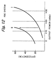
- Curve I in Fig. 12 shows the relationship between the output power of the transmission power amplifying section and the efficiency of its operation in state I as shown in Fig. 11A. Note that, if the maximum output level of the mobile station is +31dBm, the efficiency of the transmission power amplifying section will be about 60%.
- the gain of the AGC amplifier 1 is regulated to reduce the output power of the transmission power amplifying section to lower the efficiency of operation of the transmission power amplifying section. For example, the efficiency will become as low as 20 % when the output power at the output terminal of the switch circuit 23 is reduced to about +12dBm.
- the amplifier 2 is connected via the switch circuits 21, 31 and 23 to the directional coupler 5. Simultaneously, the bias circuits 24 and 25 interrupts the supply of voltage to the amplifiers 3 and 4, so that the amplifiers 3 and 4 are deactivated, thus reducing the power dissipation.
- the transmission signal entered into the AGC amplifier 1 is output by way of the route of the amplifier 2 ⁇ the switch circuit 21 ⁇ the switch circuit 23 ⁇ the directional coupler 5.
- the amplifier 2 is turned ON while the amplifiers 3 and 4 are turned OFF so that the output of the amplifier 2 is directly used as output power of the transmission power amplifying section of the mobile station.
- Curve II in Fig. 13 shows the relationship between the output power of the transmission power amplifying section and the efficiency of its operation under state II as shown in Fig. 10. It will be seen from Fig. 13 that the transmission power amplifying section shows an efficiency slightly lower than 60% when the output power is reduced to about +12dBm to 13dBm.
- the AGC amplifier 1 is regulated to adjust its gain and hence the output level of the transmission power amplifying section is adjusted in response to the change in the distance signal S 6 .
- the amplifier 3 is connected via the switch circuit 31 to the matching circuit 32 and the directional coupler 33.
- the bias control circuit 25 interrupts the supply of voltage to the amplifier 4, so that the amplifier 4 is deactivated, thus reducing the power dissipation. Consequently, as shown in Fig.
- the transmission signal entered into the AGC amplifier 1 is output by way of the route of the amplifier 2 ⁇ the switch circuit 21 ⁇ the amplifier 3 ⁇ the switch circuit 31 ⁇ the matching circuit 32 ⁇ the directional coupler 33.
- the amplifiers 2 and 3 are turned ON while the amplifier 4 is turned OFF.
- Curve III in Fig. 13 shows the relationship between the output power of the transmission power amplifying section and the efficiency of its operation under state III as shown in Fig. 10.
- the amplifier 3 is made to optimally match the PHS system in the narrow band of 1,895MHz to 1,918MHz by the matching circuit 32 and its output is sent to the directional coupler 33.
- the directional coupler 33 transmits a signal with a level of a hundredth of the transmission output level to the detector 6 and then sends the remaining transmission power as the output signal S out '.
- the second embodiment operates as a PHS terminal.
- the AGC control circuit 7a, and the AGC circuit 1 are deactivated.
- Fig. 11D all the amplifiers 2, 3 and 4 are deactivated.
- the second embodiment operates as a mobile station set having a single transmission power amplifying section that is adapted to two different frequencies of the PDC system and the PHS system, and hence provides a great advantage in terms of component mounting area and manufacturing cost over any prior art mobile stations having two transmission power amplifying sections, one for the PDC system and the other for the PHS system.
- the second embodiment shows an improved efficiency for low output operation as in the case of the first embodiment.
- the second embodiment is adapted to a dual band system of the PDC system and the PHS system, it may be modified to adapt itself to a dual band system of a global system for a mobile (GSM) system using a 900MHz band and a personal communication network (PCN) system available in Europe or a dual band system of the GSM system and the PHS system.
- GSM global system for a mobile
- PCN personal communication network
- first and second embodiments have a three-stage configuration of amplifiers for the transmission power amplifying section
- the present invention can be applied to a transmission power amplifying section having more than three or a two-stage configuration of amplifiers.
- the transmission power amplifying section can show a high efficiency for low output operation, maintaining a maximum efficiency for the maximum transmission output power level, it can operate highly efficiently over a wide output dynamic range to significantly prolong the sustainable duration of a call.
- a single transmission power amplifying section can adapt itself to the transmission of a radio wave in either of two different frequency bands to reduce the element mounting area and the manufacturing cost of the transmission power amplifying section.
Landscapes
- Engineering & Computer Science (AREA)
- Power Engineering (AREA)
- Transmitters (AREA)
- Amplifiers (AREA)
- Control Of Amplification And Gain Control (AREA)
- Mobile Radio Communication Systems (AREA)
Claims (5)
- Emetteur fixé sur une station mobile pour communiquer avec une station de base, comprenant:une section d'amplification de puissance d'émission formée par une pluralité d'amplificateurs (1, 2, 3) ;une pluralité de circuits commutateurs (21, 22, 23) chacun étant connecté à une sortie d'un desdits amplificateurs ;
etun circuit de contrôle (9", 11, 24, 25, 26), connecté auxdits amplificateurs et auxdits circuits commutateurs, caractérisé en ce que ledit circuit de contrôle est adapté pour activer au moins un des amplificateurs et actionner lesdits circuits commutateurs pour connecter en série ledit au moins un amplificateur en fonction de la distance entre ladite station mobile et ladite station de base, etledit émetteur, comprenant en outre un circuit d'adaptation (32), connecté à un desdits circuits commutateurs, pour réaliser une adaptation à une gamme de fréquences différente d'une gamme de fréquences à laquelle lesdits amplificateurs sont adaptés. - Emetteur selon la revendication 1, comprenant en outre :un amplificateur de commande automatique de gain (1) connecté à une entrée d'un premier étage desdits amplificateurs ;un premier coupleur directionnel (5) connecté à une sortie d'un dernier étage desdits circuits commutateurs ; etun second coupleur directionnel (33) connecté à une sortie dudit circuit d'adaptation.
- Emetteur selon la revendication 1, dans lequel ledit circuit de contrôle comprend :un premier circuit de contrôle (9") pour produire un signal de commande (C1, C2) en fonction de ladite distance et dudit signal de mode système ; etun second circuit de contrôle (26), connecté audit premier circuit de contrôle, pour recevoir ledit signal de commande et activer sélectivement et connecter ledit amplificateur en série entre ledit amplificateur de commande automatique de gain et un desdits coupleurs directionnels.
- Emetteur selon la revendication 1, dans lequel ledit circuit commutateur de chacun desdits étages d'amplificateur est d'un type unipolaire à deux directions.
- Emetteur selon la revendication 2, comprenant en outre :un détecteur (6) connecté auxdits premier et second coupleurs directionnels ;un comparateur (7), connecté audit détecteur et audit circuit de contrôle, pour comparer une tension de détection (VD) dudit détecteur à une tension de référence (VR) fournie par ledit circuit de contrôle, ladite tension de référence dépendant de ladite distance ; etun circuit de commande de gain automatique de la tension (7a), connecté audit comparateur, pour contrôler ledit amplificateur de contrôle de gain automatique de sorte que ladite tension de détection soit amenée à une valeur proche de ladite tension de référence.
Applications Claiming Priority (3)
| Application Number | Priority Date | Filing Date | Title |
|---|---|---|---|
| JP149229/97 | 1997-06-06 | ||
| JP14922997 | 1997-06-06 | ||
| JP14922997A JP3171141B2 (ja) | 1997-06-06 | 1997-06-06 | 移動体通信用送信機およびその制御方法 |
Publications (3)
| Publication Number | Publication Date |
|---|---|
| EP0883250A2 EP0883250A2 (fr) | 1998-12-09 |
| EP0883250A3 EP0883250A3 (fr) | 2003-03-19 |
| EP0883250B1 true EP0883250B1 (fr) | 2004-09-29 |
Family
ID=15470699
Family Applications (1)
| Application Number | Title | Priority Date | Filing Date |
|---|---|---|---|
| EP98110485A Expired - Lifetime EP0883250B1 (fr) | 1997-06-06 | 1998-06-08 | Emetteur de communications mobiles avec des amplificateurs sélectivement activés |
Country Status (6)
| Country | Link |
|---|---|
| US (1) | US6215987B1 (fr) |
| EP (1) | EP0883250B1 (fr) |
| JP (1) | JP3171141B2 (fr) |
| KR (1) | KR100293484B1 (fr) |
| CN (1) | CN1098566C (fr) |
| DE (1) | DE69826563T2 (fr) |
Cited By (1)
| Publication number | Priority date | Publication date | Assignee | Title |
|---|---|---|---|---|
| EP4143976A4 (fr) * | 2020-04-28 | 2023-11-01 | Lake Shore Cryotronics, Inc. | Systèmes et procédés de mesure de plage visant à atténuer les effets transitifs dans des mesures de matériaux à plages multiples |
Families Citing this family (70)
| Publication number | Priority date | Publication date | Assignee | Title |
|---|---|---|---|---|
| GB9811382D0 (en) * | 1998-05-27 | 1998-07-22 | Nokia Mobile Phones Ltd | A transmitter |
| JP3587346B2 (ja) * | 1998-08-07 | 2004-11-10 | 松下電器産業株式会社 | 無線通信装置および無線通信装置における送信電力制御方法 |
| JP3587347B2 (ja) * | 1998-08-07 | 2004-11-10 | 松下電器産業株式会社 | 無線通信装置および無線通信装置における送信電力制御方法 |
| US6418304B1 (en) * | 1998-09-16 | 2002-07-09 | Lucent Technologies Inc. | Method and apparatus for improving efficiency of high-power linear amplifier |
| FI106412B (fi) | 1998-11-10 | 2001-01-31 | Nokia Mobile Phones Ltd | Lineaarinen tehovahvistinjärjestely ja menetelmä sen käyttämiseksi |
| JP2000196521A (ja) * | 1998-12-25 | 2000-07-14 | Matsushita Electric Ind Co Ltd | 無線通信装置及び無線通信装置における送信電力制御方法 |
| US6615028B1 (en) * | 1998-12-29 | 2003-09-02 | Skyworks Solutions, Inc. | System and method for selecting amplifiers in a communications device |
| EP1032120A3 (fr) * | 1999-02-26 | 2003-07-30 | Matsushita Electric Industrial Co., Ltd. | Amplificateur de puissance, méthode de commande de la puissance d'un amplificateur de puissance et équipement de communication |
| WO2000059119A1 (fr) * | 1999-03-25 | 2000-10-05 | Siemens Aktiengesellschaft | Terminal de reseau mobile |
| JP4062816B2 (ja) * | 1999-05-13 | 2008-03-19 | 株式会社デンソー | 送信電力制御回路 |
| US6763470B1 (en) * | 1999-05-19 | 2004-07-13 | Globespanvirata, Inc. | System and method for dynamically amplifying a delayed analog signal based on amplitude information obtained from its digital representation |
| US6556814B1 (en) * | 1999-07-22 | 2003-04-29 | Motorola, Inc. | Memory-based amplifier load adjust system |
| JP3739614B2 (ja) * | 1999-11-24 | 2006-01-25 | アルプス電気株式会社 | 出力電力調整を行う送信機 |
| KR20010059473A (ko) * | 1999-12-30 | 2001-07-06 | 윤종용 | 이동통신 단말기의 송신장치 및 방법 |
| US6721368B1 (en) | 2000-03-04 | 2004-04-13 | Qualcomm Incorporated | Transmitter architectures for communications systems |
| US6920334B1 (en) * | 2000-03-24 | 2005-07-19 | International Business Machines Corporation | Method and apparatus for providing gain control feedback in RF amplifiers |
| JP2001284998A (ja) * | 2000-03-31 | 2001-10-12 | Mitsubishi Electric Corp | 無線送信装置 |
| JP2001326537A (ja) | 2000-05-16 | 2001-11-22 | Mitsubishi Electric Corp | 高効率増幅器、当該高効率増幅器を備える無線送信装置および当該高効率増幅器を評価するための測定装置 |
| JP4610697B2 (ja) * | 2000-06-13 | 2011-01-12 | パナソニック株式会社 | 送信電力制御方法及び無線通信装置 |
| FR2812141B1 (fr) * | 2000-07-21 | 2003-01-10 | Thomson Multimedia Sa | Bloc d'amplification de signaux rf, dispositif d'emission de signaux rf et terminal-antenne d'emission de signaux rf |
| US6670849B1 (en) * | 2000-08-30 | 2003-12-30 | Skyworks Solutions, Inc. | System for closed loop power control using a linear or a non-linear power amplifier |
| JP3848068B2 (ja) * | 2000-09-12 | 2006-11-22 | 株式会社エヌ・ティ・ティ・ドコモ | Cdma無線送信装置、cdma無線送受信システムおよびcdma無線送信装置の送信電力制御方法ならびにcdma無線送受信システムにおける無線送信装置の送信電力制御方法 |
| KR20020027052A (ko) * | 2000-10-04 | 2002-04-13 | 송재인 | 무선 기기의 출력 자동 조정 방법 |
| FR2815510B1 (fr) * | 2000-10-17 | 2005-02-25 | Sagem | Telephone mobile avec emetteur perfectionne |
| DE60035598T2 (de) | 2000-10-27 | 2008-06-19 | Stmicroelectronics N.V. | Verfahren und Vorrichtung zur Leistungsregelung eines Mobilfunktelefons |
| US6653898B2 (en) * | 2000-12-28 | 2003-11-25 | Samsung Electronics Co., Ltd. | High efficiency stage-switching CDMA power amplifier |
| US6961368B2 (en) * | 2001-01-26 | 2005-11-01 | Ericsson Inc. | Adaptive antenna optimization network |
| TW503345B (en) * | 2001-03-26 | 2002-09-21 | Mediatec Inc | Power controller |
| WO2002097983A1 (fr) * | 2001-05-31 | 2002-12-05 | Nokia Corporation | Circuit de variation de puissance, emetteur radio, terminal radio et procede de variation de la puissance des signaux |
| WO2002104043A2 (fr) * | 2001-06-19 | 2002-12-27 | Harris Corporation | Procede et systeme permettant de determiner les reglages operationnels nominaux de la station deportee pour assurer une interference de bruit minime de la station de base |
| KR20030016449A (ko) * | 2001-08-16 | 2003-03-03 | 삼성전자주식회사 | 무선 송신기의 송신 전력 제어장치 |
| US6819941B2 (en) | 2001-10-11 | 2004-11-16 | Rf Micro Devices, Inc. | Single output stage power amplification for multimode applications |
| JP2003124754A (ja) * | 2001-10-18 | 2003-04-25 | Hitachi Ltd | 高周波増幅器 |
| TW516748U (en) * | 2001-10-26 | 2003-01-01 | Kye Systems Corp | Wireless transmitting circuit with adjustable radio frequency transmitting power |
| JP2004159221A (ja) * | 2002-11-08 | 2004-06-03 | Renesas Technology Corp | 通信用半導体集積回路および無線通信システム |
| JP4160381B2 (ja) * | 2002-12-27 | 2008-10-01 | ローム株式会社 | 音声出力装置を有する電子装置 |
| JP3922571B2 (ja) * | 2003-03-26 | 2007-05-30 | ソニー株式会社 | 情報処理装置および情報処理方法、記録媒体、並びに、プログラム |
| US7170341B2 (en) * | 2003-08-05 | 2007-01-30 | Motorola, Inc. | Low power consumption adaptive power amplifier |
| US7228135B2 (en) * | 2003-08-12 | 2007-06-05 | Yury Alexeevich Gromakov | Method for cellular communications |
| JP4521806B2 (ja) * | 2003-09-11 | 2010-08-11 | ソニー・エリクソン・モバイルコミュニケーションズ株式会社 | 電力増幅装置および送信装置 |
| US7623896B2 (en) * | 2004-02-04 | 2009-11-24 | Sharp Kabushiki Kaisha | Wireless communication circuit and wireless communication apparatus using the same |
| US7379714B2 (en) * | 2004-04-02 | 2008-05-27 | Interdigital Technology Corporation | Method and apparatus for dynamically adjusting a transmitter's impedance |
| KR20050100300A (ko) * | 2004-04-13 | 2005-10-18 | 엘지전자 주식회사 | 이동통신 단말기의 전력증폭기모드 선택장치 |
| US7292096B2 (en) * | 2004-06-21 | 2007-11-06 | Samsung Electronics Co., Ltd. | Amplifier |
| JP4487768B2 (ja) * | 2004-12-27 | 2010-06-23 | 日本電気株式会社 | 無線送信装置及びその送信電力調整方法 |
| US7345534B2 (en) * | 2005-05-31 | 2008-03-18 | M/A-Com Eurotec Bv | Efficient power amplification system |
| JP4584062B2 (ja) * | 2005-07-21 | 2010-11-17 | セイコーインスツル株式会社 | 携帯型電子機器 |
| US20070076666A1 (en) * | 2005-10-03 | 2007-04-05 | Riveiro Juan C | Multi-Wideband Communications over Power Lines |
| US7808985B2 (en) * | 2006-11-21 | 2010-10-05 | Gigle Networks Sl | Network repeater |
| US8406239B2 (en) * | 2005-10-03 | 2013-03-26 | Broadcom Corporation | Multi-wideband communications over multiple mediums |
| EP1770870B1 (fr) * | 2005-10-03 | 2019-04-03 | Avago Technologies International Sales Pte. Limited | Procédé et dispositif de communication sur ligne d'alimentation |
| US8213895B2 (en) * | 2005-10-03 | 2012-07-03 | Broadcom Europe Limited | Multi-wideband communications over multiple mediums within a network |
| US7933567B2 (en) * | 2006-01-26 | 2011-04-26 | Qualcomm, Incorporated | Method and apparatus for achieving linear monotonic output power |
| US7860146B2 (en) * | 2006-07-06 | 2010-12-28 | Gigle Networks, Inc. | Adaptative multi-carrier code division multiple access |
| US8885814B2 (en) | 2006-07-25 | 2014-11-11 | Broadcom Europe Limited | Feedback impedance control for driving a signal |
| EP1892827A1 (fr) * | 2006-08-24 | 2008-02-27 | Alcatel Lucent | Amplificateur de puissance multi-standard à bande monofréquence |
| JP5022792B2 (ja) * | 2007-07-02 | 2012-09-12 | 株式会社日立国際電気 | Dcdcコンバータユニット、電力増幅器、及び基地局装置 |
| US8619639B2 (en) | 2007-07-06 | 2013-12-31 | Lantiq Deutschland Gmbh | Power detector radio frequency multiplexer |
| US7795973B2 (en) * | 2008-10-13 | 2010-09-14 | Gigle Networks Ltd. | Programmable gain amplifier |
| JP4957734B2 (ja) * | 2009-02-10 | 2012-06-20 | ソニー株式会社 | 受信装置、撮像装置及び受信方法 |
| US8971830B2 (en) * | 2009-05-12 | 2015-03-03 | Qualcomm Incorporated | Multi-mode multi-band power amplifier module |
| US8487705B2 (en) | 2010-05-26 | 2013-07-16 | Triquint Semiconductor, Inc. | Protection circuit for radio frequency power amplifier |
| CN102420711B (zh) * | 2010-09-28 | 2014-04-30 | 鸿富锦精密工业(深圳)有限公司 | 网络通信设备及其侦测负载异常的方法 |
| TWI450509B (zh) * | 2010-10-07 | 2014-08-21 | Hon Hai Prec Ind Co Ltd | 網路通訊設備及其偵測負載異常的方法 |
| RU2481696C9 (ru) * | 2011-05-05 | 2013-09-10 | Евгений Васильевич Прокофьев | Генератор автоколебаний прокофьева |
| CN102355204B (zh) * | 2011-05-20 | 2014-04-16 | 深圳市纳芯威科技有限公司 | 一种音频功放自动切换电路及功放芯片 |
| US8538368B1 (en) * | 2011-11-14 | 2013-09-17 | Triquint Semiconductor, Inc. | Dynamic power limiter circuit |
| US8829997B1 (en) | 2012-10-23 | 2014-09-09 | M/A-Com Technology Solutions Holdings, Inc. | Monolithic integrated power regulation for power control and/or bias control |
| CN107733379B (zh) * | 2016-08-11 | 2021-08-03 | 格兰康希通信科技(上海)有限公司 | 射频放大器输出端失配检测电路及其检测方法 |
| JP2019092131A (ja) * | 2017-11-17 | 2019-06-13 | 株式会社村田製作所 | 電力増幅モジュール |
Family Cites Families (21)
| Publication number | Priority date | Publication date | Assignee | Title |
|---|---|---|---|---|
| JPS5851453B2 (ja) | 1980-09-29 | 1983-11-16 | 日本電信電話株式会社 | 送信装置 |
| US4485486A (en) * | 1982-08-03 | 1984-11-27 | Motorola, Inc. | Method and apparatus for assigning duplex radio channels and scanning duplex radio channels assigned to mobile and portable radio telephones in a cellular radiotelephone communications system |
| US4598252A (en) * | 1984-07-06 | 1986-07-01 | Itt Corporation | Variable gain power amplifier |
| US4755769A (en) * | 1987-05-20 | 1988-07-05 | General Electric Company | Composite amplifier with efficient power reduction |
| JPH02246531A (ja) * | 1989-03-20 | 1990-10-02 | Fujitsu Ltd | 送信電力可変形送信機の送信断検出回路 |
| JP2746685B2 (ja) * | 1989-09-06 | 1998-05-06 | 富士通株式会社 | 送信出力制御回路 |
| JPH0425220A (ja) * | 1990-05-21 | 1992-01-29 | Toshiba Corp | 自動電力制御回路 |
| JPH0454006A (ja) * | 1990-06-22 | 1992-02-21 | Fujitsu Ltd | 増幅装置 |
| KR950000054B1 (ko) * | 1990-07-27 | 1995-01-07 | 가부시끼가이샤 도시바 | 자동파워 콘트롤장치 |
| US5129098A (en) * | 1990-09-24 | 1992-07-07 | Novatel Communication Ltd. | Radio telephone using received signal strength in controlling transmission power |
| US5251328A (en) * | 1990-12-20 | 1993-10-05 | At&T Bell Laboratories | Predistortion technique for communications systems |
| NZ255617A (en) * | 1992-09-04 | 1996-11-26 | Ericsson Telefon Ab L M | Tdma digital radio: measuring path loss and setting transmission power accordingly |
| JP3444653B2 (ja) * | 1994-06-09 | 2003-09-08 | 三菱電機株式会社 | 電力増幅器 |
| US5758269A (en) * | 1995-03-30 | 1998-05-26 | Lucent Technologies Inc. | High-efficient configurable power amplifier for use in a portable unit |
| US5661434A (en) * | 1995-05-12 | 1997-08-26 | Fujitsu Compound Semiconductor, Inc. | High efficiency multiple power level amplifier circuit |
| US5862461A (en) * | 1995-08-31 | 1999-01-19 | Sony Corporation | Transmitting apparatus and method of adjusting gain of signal to be transmitted, and receiving apparatus and method of adjusting gain of received signal |
| US5852770A (en) * | 1995-09-19 | 1998-12-22 | Sanyo Electric Co., Ltd. | Transmission power control device for a portable terminal |
| US5872481A (en) * | 1995-12-27 | 1999-02-16 | Qualcomm Incorporated | Efficient parallel-stage power amplifier |
| JPH1022756A (ja) * | 1996-07-04 | 1998-01-23 | Mitsubishi Electric Corp | 無線送信機およびその送信制御方法 |
| US5834975A (en) * | 1997-03-12 | 1998-11-10 | Rockwell Science Center, Llc | Integrated variable gain power amplifier and method |
| US5923213A (en) * | 1997-07-09 | 1999-07-13 | U.S. Philips Corporation | Digitally gain-controlled amplifying device, and camera using such a device |
-
1997
- 1997-06-06 JP JP14922997A patent/JP3171141B2/ja not_active Expired - Fee Related
-
1998
- 1998-06-05 CN CN98102062A patent/CN1098566C/zh not_active Expired - Fee Related
- 1998-06-05 US US09/090,883 patent/US6215987B1/en not_active Expired - Lifetime
- 1998-06-05 KR KR1019980020964A patent/KR100293484B1/ko not_active Expired - Fee Related
- 1998-06-08 EP EP98110485A patent/EP0883250B1/fr not_active Expired - Lifetime
- 1998-06-08 DE DE69826563T patent/DE69826563T2/de not_active Expired - Fee Related
Cited By (5)
| Publication number | Priority date | Publication date | Assignee | Title |
|---|---|---|---|---|
| EP4143976A4 (fr) * | 2020-04-28 | 2023-11-01 | Lake Shore Cryotronics, Inc. | Systèmes et procédés de mesure de plage visant à atténuer les effets transitifs dans des mesures de matériaux à plages multiples |
| US11959991B2 (en) | 2020-04-28 | 2024-04-16 | Lake Shore Cryotronics, Inc. | Hybrid digital and analog signal generation systems and methods |
| US11982730B2 (en) | 2020-04-28 | 2024-05-14 | Lake Shore Cryotronics, Inc. | Ranging systems and methods for decreasing transitive effects in multi-range materials measurements |
| US12287390B2 (en) | 2020-04-28 | 2025-04-29 | Lake Shore Cryotronics, Inc. | Hybrid digital and analog signal generation systems and methods |
| US12429547B2 (en) | 2020-04-28 | 2025-09-30 | Lake Shore Cryotronics, Inc. | Ranging systems and methods for decreasing transitive effects in multi-range materials measurements |
Also Published As
| Publication number | Publication date |
|---|---|
| KR19990006729A (ko) | 1999-01-25 |
| EP0883250A2 (fr) | 1998-12-09 |
| DE69826563T2 (de) | 2006-02-23 |
| DE69826563D1 (de) | 2004-11-04 |
| US6215987B1 (en) | 2001-04-10 |
| KR100293484B1 (ko) | 2001-09-17 |
| CN1098566C (zh) | 2003-01-08 |
| CN1202046A (zh) | 1998-12-16 |
| JPH10341172A (ja) | 1998-12-22 |
| JP3171141B2 (ja) | 2001-05-28 |
| EP0883250A3 (fr) | 2003-03-19 |
Similar Documents
| Publication | Publication Date | Title |
|---|---|---|
| US6215987B1 (en) | Mobile communication transmitter capable of selectively activating amplifiers | |
| RU2252483C2 (ru) | Способ и устройство усиления мощности передачи беспроводного телефона при пониженном энергопотреблении | |
| US6169449B1 (en) | Transmission power control circuit capable of varying electric power over a wide range | |
| US6515541B2 (en) | Multi-level power amplifier | |
| KR100353313B1 (ko) | 전력제어회로및이동전화의전력효율을향상시키는방법 | |
| US8546980B2 (en) | Radio-frequency module and radio communication system | |
| US7868700B2 (en) | Method and apparatus for reducing current consumption of MIMO systems | |
| US6972618B2 (en) | High efficiency power amplifier with multiple power modes | |
| JPH10173453A (ja) | 高周波可変利得増幅装置および無線通信装置 | |
| US6252463B1 (en) | High-frequency switch, adjustable high-frequency switch, and adjustable high-frequency power amplifier | |
| US6950637B2 (en) | Power rate enhancement circuit for an RF power amplifier in a dual mode mobile phone | |
| JP2006025062A (ja) | 高周波スイッチ回路 | |
| GB2334168A (en) | Dual band amplifier for a radiotelephone transmitter | |
| EP0874452B1 (fr) | Circuit de réception pour téléphone cellulaire | |
| JP3235580B2 (ja) | 高効率増幅器 | |
| US6760604B2 (en) | Portable radio transceiver having shared power source for audio and RF amplifiers | |
| US6518840B1 (en) | Circuit for linearizing the power control profile of a BiCMOS power amplifier | |
| JP2000165311A (ja) | 携帯端末の出力回路 | |
| US6445729B1 (en) | Radio signal transceiver apparatus | |
| US6842072B1 (en) | Power gain reduction circuit for power amplifiers | |
| KR20250016324A (ko) | 적응형 바이어싱을 갖는 도허티 증폭기 | |
| KR100654644B1 (ko) | 최적화된 전력 효율을 갖는 전력 증폭기 | |
| US7190228B2 (en) | Gain control device of transmitter in mobile communication terminal and method thereof | |
| JPH11145748A (ja) | 電力増幅回路 | |
| KR100757706B1 (ko) | 선택적 전압 제어를 이용한 고효율 바이패스 스위칭 다중모드 전력 증폭 장치 |
Legal Events
| Date | Code | Title | Description |
|---|---|---|---|
| PUAI | Public reference made under article 153(3) epc to a published international application that has entered the european phase |
Free format text: ORIGINAL CODE: 0009012 |
|
| AK | Designated contracting states |
Kind code of ref document: A2 Designated state(s): AT BE CH CY DE DK ES FI FR GB GR IE IT LI LU MC NL PT SE |
|
| AX | Request for extension of the european patent |
Free format text: AL;LT;LV;MK;RO;SI |
|
| RAP1 | Party data changed (applicant data changed or rights of an application transferred) |
Owner name: NEC COMPOUND SEMICONDUCTOR DEVICES, LTD. |
|
| PUAL | Search report despatched |
Free format text: ORIGINAL CODE: 0009013 |
|
| AK | Designated contracting states |
Kind code of ref document: A3 Designated state(s): AT BE CH CY DE DK ES FI FR GB GR IE IT LI LU MC NL PT SE |
|
| AX | Request for extension of the european patent |
Extension state: AL LT LV MK RO SI |
|
| 17P | Request for examination filed |
Effective date: 20030618 |
|
| 17Q | First examination report despatched |
Effective date: 20030909 |
|
| AKX | Designation fees paid |
Designated state(s): DE GB |
|
| GRAP | Despatch of communication of intention to grant a patent |
Free format text: ORIGINAL CODE: EPIDOSNIGR1 |
|
| GRAS | Grant fee paid |
Free format text: ORIGINAL CODE: EPIDOSNIGR3 |
|
| GRAA | (expected) grant |
Free format text: ORIGINAL CODE: 0009210 |
|
| AK | Designated contracting states |
Kind code of ref document: B1 Designated state(s): DE GB |
|
| REG | Reference to a national code |
Ref country code: GB Ref legal event code: FG4D |
|
| REG | Reference to a national code |
Ref country code: IE Ref legal event code: FG4D |
|
| REF | Corresponds to: |
Ref document number: 69826563 Country of ref document: DE Date of ref document: 20041104 Kind code of ref document: P |
|
| PLBE | No opposition filed within time limit |
Free format text: ORIGINAL CODE: 0009261 |
|
| STAA | Information on the status of an ep patent application or granted ep patent |
Free format text: STATUS: NO OPPOSITION FILED WITHIN TIME LIMIT |
|
| 26N | No opposition filed |
Effective date: 20050630 |
|
| REG | Reference to a national code |
Ref country code: GB Ref legal event code: 732E |
|
| PGFP | Annual fee paid to national office [announced via postgrant information from national office to epo] |
Ref country code: GB Payment date: 20090603 Year of fee payment: 12 Ref country code: DE Payment date: 20090604 Year of fee payment: 12 |
|
| GBPC | Gb: european patent ceased through non-payment of renewal fee |
Effective date: 20100608 |
|
| PG25 | Lapsed in a contracting state [announced via postgrant information from national office to epo] |
Ref country code: DE Free format text: LAPSE BECAUSE OF NON-PAYMENT OF DUE FEES Effective date: 20110101 |
|
| PG25 | Lapsed in a contracting state [announced via postgrant information from national office to epo] |
Ref country code: GB Free format text: LAPSE BECAUSE OF NON-PAYMENT OF DUE FEES Effective date: 20100608 |