EP0884776A2 - Structure isolante pour cellule DRAM avec capacité ensillonée - Google Patents
Structure isolante pour cellule DRAM avec capacité ensillonée Download PDFInfo
- Publication number
- EP0884776A2 EP0884776A2 EP98109820A EP98109820A EP0884776A2 EP 0884776 A2 EP0884776 A2 EP 0884776A2 EP 98109820 A EP98109820 A EP 98109820A EP 98109820 A EP98109820 A EP 98109820A EP 0884776 A2 EP0884776 A2 EP 0884776A2
- Authority
- EP
- European Patent Office
- Prior art keywords
- layer
- trench
- transistor
- substrate
- forming
- Prior art date
- Legal status (The legal status is an assumption and is not a legal conclusion. Google has not performed a legal analysis and makes no representation as to the accuracy of the status listed.)
- Withdrawn
Links
Images


Classifications
-
- H—ELECTRICITY
- H10—SEMICONDUCTOR DEVICES; ELECTRIC SOLID-STATE DEVICES NOT OTHERWISE PROVIDED FOR
- H10B—ELECTRONIC MEMORY DEVICES
- H10B12/00—Dynamic random access memory [DRAM] devices
- H10B12/30—DRAM devices comprising one-transistor - one-capacitor [1T-1C] memory cells
- H10B12/37—DRAM devices comprising one-transistor - one-capacitor [1T-1C] memory cells the capacitor being at least partially in a trench in the substrate
-
- H—ELECTRICITY
- H10—SEMICONDUCTOR DEVICES; ELECTRIC SOLID-STATE DEVICES NOT OTHERWISE PROVIDED FOR
- H10B—ELECTRONIC MEMORY DEVICES
- H10B12/00—Dynamic random access memory [DRAM] devices
- H10B12/01—Manufacture or treatment
- H10B12/02—Manufacture or treatment for one transistor one-capacitor [1T-1C] memory cells
- H10B12/03—Making the capacitor or connections thereto
- H10B12/038—Making the capacitor or connections thereto the capacitor being in a trench in the substrate
Definitions
- the invention generally relates to device fabrication such as random access memories and, more particularly, to reducing oxidation stress at the shallow trench isolation interface.
- insulating, semiconducting, and conducting layers are formed on a substrate.
- the layers are patterned to create features and spaces.
- the minimum dimension or feature size (F) of the features and spaces depend on the resolution capability of the lithographic systems.
- the features and spaces are patterned so as to form devices, such as transistors, capacitors, and resistors. These devices are then interconnected to achieve a desired electrical function.
- the formation and patterning of the various device layers are achieved using conventional fabrication techniques, such as oxidation, implantation, deposition, epitaxial growth of silicon, lithography, and etching. Such techniques are described in S.M. Sze, VLSI Technology , 2nd ed., New York, McGraw-Hill, 1988, which is herein incorporated by reference for all purposes.
- Random access memories such as dynamic random access memories (DRAMs) comprise memory cells that are configured in rows and columns to provide storage of information.
- DRAMs dynamic random access memories
- One type of memory cells includes, for example, a transistor connected to a trench capacitor.
- the capacitor is referred to as the "node" when activated, the transistor allows information to be read or written into the capacitor.
- the invention generally relates the reduction of oxidation stress at the shallow trench isolation interface.
- a random access memory cell implemented with a trench capacitor is provided with a raised shallow trench isolation.
- the trench capacitor which is formed below the top surface of a substrate, such as a silicon wafer, serves as the storage node of the memory cell.
- the top surface of the raised shallow trench isolation is raised above the top surface of the silicon substrate to reduce oxidation stress.
- the amount that the top surface of the shallow trench isolation is raised is sufficient to prevent the bottom of the divot formed during processing from being below the silicon surface.
- the present invention relates to reducing oxidation stress during the fabrication of devices.
- the present invention is described in the context of fabricating a trench capacitor DRAM cell.
- a description of the fabrication of a conventional trench capacitor DRAM cell is provided.
- a conventional trench capacitor DRAM cell 100 is shown.
- Such conventional trench capacitor DRAM cell is described in, for example, Nesbit et al., A 0.6 ⁇ m 2 256Mb Trench DRAM Cell With Self-Aligned BuriEd Strap (BEST) , IEDM 93-627, which is herein incorporated by reference for all purposes.
- BEST Self-Aligned BuriEd Strap
- IEDM 93-627 Self-Aligned BuriEd Strap
- the DRAM cell comprises a trench capacitor 160 formed in a substrate 101.
- the substrate is lightly doped with a dopant having a first conductivity.
- the trench is filled with, typically, polysilicon (poly) 161 heavily doped with dopants having a second conductivity.
- the poly serves as one plate of the capacitor.
- the other plate of the capacitor is formed by a buried plate 165, also having a second conductivity.
- the DRAM cell also comprises a transistor 110.
- the transistor includes a gate 112, source 113, and drain 14.
- the drain and source are formed by implanting dopants having a second conductivity.
- Connection of the transistor to the capacitor is achieved via a strap 125.
- Tie strap is formed by providing dopants having the same conductivity as the source.
- a buried strap is employed to connect the trench to the capacitor.
- Other techniques, such as a surface strap, for connecting the transistor to the capacitor are also useful.
- a collar 168 is formed at a top portion of the trench. Punchthrough is undesirable as it affects the operability of the cell.
- a buried well 170 also having dopants of the second conductivity, is provided below the surface of the substrate with a peak concentration of dopants at about the bottom of the collar. Typically, the well is lightly doped.
- the buried well serves to connect the buried plates of the individual DRAM cells in the array together.
- the gate and source form a wordline and bitline, respectively, in the DRAM array.
- Activation of the transistor by providing the appropriate voltage at the wordline and bitline junction enables data to be written or read from the trench capacitor.
- a shallow trench isolation (STI) 180 is provided to isolate the DRAM cell from other cells or devices.
- a wordline 120 which is not connected to the cell, is typically formed over the trench.
- Wordline 120 is referred to as the "passing wordline”.
- the passing wordline is isolated from the trench by the STI.
- Such a configuration is referred to as a folded bitline architecture.
- Other bitline architectures such as open or open-folded are also useful.
- the first conductivity is positive (p) and the second conductivity is negative (n).
- p positive
- n negative
- DRAM cells formed in a n-type substrate with p-type poly filled trenches are also useful. Further, it is possible to heavily or lightly doped the substrate, wells, buried plate, and other elements of the DRAM cell with impurity atoms to achieve the desired electrical characteristics.
- Figs. 2a-2g depict a part of process of forming the conventional DRAM cell.
- a substrate 201 for forming the DRAM cell is provided.
- the major surface of the substrate is not critical and any suitable orientation such as an (100), (110), or (111) is useful.
- the substrate is lightly doped with p-type dopants (p - ).
- a pad stack 230 is formed on the surface of the substrate.
- the pad stack comprises various layers functioning as an etch mask, etch stop, and/or chemical mechanical polish stop layers.
- the pad stack comprises a pad oxide layer 231, nitride layer 232, and TEOS mask layer (not shown).
- a trench 210 is formed in the substrate. Techniques for forming the trench is described in, for example, Müller et al., Trench Storage Node Technology for Gigabit DRAM Generation , IEDM 96-507, which is already herein incorporated by reference for all purposes.
- the trench is filled with heavily doped n-type (n + ) poly 214.
- the n + poly serves as one plate of the capacitors.
- a n + buried plate 215 surrounds the bottom portion of the trench and serves as the other plate of the capacitor.
- the trench and buried plate are isolated from each other by a node dielectric layer 212.
- the node dielectric layer comprises nitride and oxide layers.
- a collar 220 is formed in an upper portion of the trench.
- the collar comprises a dielectric material such as, for example TEOS.
- a buried N - well 280 is provided for connecting the other trenches in the array together.
- the surface of the substrate have been polished by, for example, Chemical Mechanical Polishing (CMP).
- CMP Chemical Mechanical Polishing
- the nitride layer 232 serves as an CMP stop layer, causing the CMP to stop once it reaches the nitride layer.
- the poly that covers the surface of the substrate is planarized, leaving a substantially planar surface between the nitride and poly for subsequent processing.
- the trench is recessed, by for example, reactive ion etching (RIE).
- RIE reactive ion etching
- the poly is recessed to about 150nm below the silicon surface.
- a clean step is performed to remove any native oxide that may have formed on the silicon trench sidewall.
- the clean step comprises, for example, a wet etch selective to silicon.
- the clean step removes the oxide from the trench sidewalls as well as a to portion of the collar, recessing it below the N + poly. As a result, a gap between the silicon and poly sidewalls 225 and 227 is formed.
- a poly layer 240 is deposited on the substrate, covering the nitride layer and top portion of the trench.
- the poly layer is an intrinsic or undoped poly layer.
- the poly layer is planarized down to the nitride layer 232. After planarization, the poly in the trench is recessed to, for example, about 50 nm below the surface of the substrate, leaving a strap of about 100 nm above the n + trench poly.
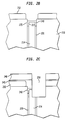
- Fig. 2c shows the process for defining the active area of the DRAM cell.
- an anti-reflective coating (ARC) layer 245 is deposited on the substrate surface, covering the nitride layer 232 and strap 240.
- ARC is used to improve the resolution of the lithographic process for defining the active area (AA).
- a resist layer 246 is formed above the ARC layer, serving as an AA etch mask.
- the active region is then defined by conventional lithographic technique.
- the nonactive region 250 of the cell is then anisotropically etched by, for example, RIE. As shown, the nonactive region overlaps a portion of the trench. Typically, the nonactive region is etched below the top of the oxide collar.
- the nonactive region is etched about 250-400 nm below the silicon surface.
- the nonactive region is the region where a STI is to be formed.
- a nitride liner 255 is provided to protect the nonactive region.
- a passivation oxide is thermally grown on the exposed silicon prior to forming the nitride liner.
- the nitride liner is formed by, for example low pressure chemical vapor deposition (LPCVD). As shown, the nitride liner is formed over the substrate surface, covering the nitride layer and nonactive STI region.
- LPCVD low pressure chemical vapor deposition
- a dielectric material such as, for example, TEOS on the surface of the substrate to sufficiently fill the nonactive region 250. Since the TEOS layer is conformal, a planarization scheme is employed to result in a planar surface for subsequent processing. Such scheme, for example, is described in Nag et al., Comparative Evaluation of Gap-Fill Dielectrics in Shallow Trench Isolation for Sub-0.25 ⁇ m Technologies , IEDM 96-841, which is herein incorporated by reference for all purposes. The surface of the substrate is polished so that the STI and nitride layer are substantially planar.
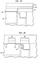
- Fig. 2e shows the process for forming the access transistor of the DRAM cell.
- the pad nitride layer is removed by, for example, wet chemical etch.
- the wet chemical etch is selective to oxide.
- an overetch is employed.
- the nitride liner at the top of the STI also gets recessed, forming a divot 257.
- the pad oxide is also removed at this point by wet chemical selective to silicon.
- the divot formed during the nitride etch exposes the oxide sidewalls on each side of the nitride liner. As such, the subsequent oxide etches further expand the divot laterally into the corner of the active area.
- an oxide (not shown) layer is then formed on the surface of the wafer.
- the oxide layer referred to as a "gate sacrificial layer" serves as a screen oxide for subsequent implants. Additionally, the gate sacrificial layer reduces divot or rounds the STI corner.
- a resist layer (not shown) is deposited on top of the oxide layer and appropriately patterned to expose the P-well region.
- P-type dopants such as boron (B) are implanted into the well region.
- the dopants are implanted sufficiently deep to prevent punchthrough.
- the dopant profile is tailored to achieve the desired electrical characteristics, e.g., gate threshold voltage (V t ).
- n-wells for n-channel support circuitry are also formed.
- CMOS complimentary metal oxide silicon
- n-wells are formed. Formation of n-wells require additional lithographic and implant steps for defining and forming the N wells. As with the p-wells, the profile of the n-wells are tailored to achieve the desired electrical characteristics. After the wells have been form, the gate sacrificial layer is removed.
- a gate oxidation layer 262 is formed and patterned to cover the region where the transistor is to be formed.
- Poly 267, WSi x 268, and nitride 269 layers are then formed over the surface of the substrate. As can be seen, the divot is filled with poly as well. Referring to Fig. 2g, these layers are then patterned to form a gate stack for a transistor 270 of the DRAM cell.
- a passing gate stack 280 is typically formed over the trench and isolated therefrom by the STI.
- Drain 271 and source 272 are formed by implanting dopants having the appropriate profile to achieve the desired operating characteristics. To improve diffusion and alignment of the source and drain to the gate, nitride spacers (not shown) may be employed.
- a strap 273 is created by outdiffusing dopants from the strap poly 240.
- the divot 257 formed near the corner of the active region adversely affects the operability of DRAM integrated circuit, such as parasitic corner conduction.
- a DRAM cell comprises a trench capacitor 360 and a transistor 310. Since the trench capacitor is similar to that described in Fig. 1, only the top portion is shown.
- the transistor 310 is a n-channel transistor.
- the transistor includes a gate 312, source 313, and drain 314.
- the drain and source are formed by implanting n-type dopants. Connection of the transistor to the capacitor is achieved via a doped region 325.
- the doped region is formed by diffusing n-type dopants from the trench.
- a dielectric collar 368 is provided to prevent vertical punchthrough between the strap and buried plate (not shown).
- a raised STI is provided to isolate the DRAM cell from other DRAM cells or devices.
- the depth of the raised STI is similar to that of a conventional STI.
- a top surface of the raised STI is located above the plane of the silicon substrate surface. The distance that top surface is raised above the substrate surface is sufficient to effectively reduce formation of divots below the silicon surface in order to reduce corner reduction.
- the distance that the top surface of the raised STI is raised is about ⁇ 100 nm.
- the distance is about 20 - 100 nm, more preferably about 40 - 80 nm, and even more preferably about 50 - 70 nm.
- the distance that the top surface of the raised STI is raised is about 50 nm.
- the formation of divots results in parasitic corner conduction.
- the present invention prevents the formation of divots by raising the surface of the STI above the substrate surface.
- the use of the raised STI advantageously eliminates the need of a nitride liner which also contributes to divot formation.
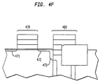
- Figs. 4a-4f show the process for forming a DRAM cell with a raised STI.
- a trench capacitor 410 is formed in a substrate 401.
- the substrate is lightly doped with p-type dopants (p - ).
- a pad stack 430 is formed on the surface of the substrate.
- the pad stack comprises various layers that serve as a etch mask, etch stop, and/or chemical mechanical polish stop layers.
- the pad stack comprises a pad oxide layer 431, nitride layer 432, and TEOS mask layer (not shown).
- the trench 410 is formed by conventional techniques. Such techniques are described in, for example, Nesbit et al., A 0.6 ⁇ m 2 256Mb Trech DRAM Cell With Self-Aligned BuriEd Strap (BEST) , IEDM 93-627, which is already herein incorporated by reference for all purposes.
- the trench is filled with N + poly 414.
- a collar 420 comprising a dielectric material such as, for example TEOS, is provided in an upper portion of the trench.
- a layer of intrinsic poly 440 is formed and recessed to above the collar and doped poly. Typically, the poly is recessed to, for example, about 50 nm below the surface of the substrate, leaving a strap 440 of, for example, about 100 nm above the N + trench poly.
- a layer of oxide is formed over the substrate surface, covering the pad stack and filling the opening above the trench.
- the oxide layer is formed by low pressure chemical vapor deposition (LPCVD).
- LPCVD low pressure chemical vapor deposition
- the oxide is densified. Densification of the oxide is achieved by an anneal of about 900 - 100°C for about 10 - 60 minutes in and inert ambient such as Argon or nitrogen.
- the CMP results in a thin oxide layer 480 on top of the poly, providing isolation for the trench.
- the pad nitride and pad oxide layers are removed by, for example, a wet etch.
- a sacrificial oxide layer (not shown) is then formed on the surface of the wafer.
- the oxide layer serves as a screen oxide layer for implants.
- P-type well region for the n-channel access transistor of the DRAM cell is formed. This is achieved by, for example, depositing a resist layer (not shown) on top of the oxide layer and appropriately patterning it to expose the p-well region. P-type dopants, such as boron (B) are implanted into the well region. The dopants are implanted sufficiently deep to prevent punchthrough. The dopant profile is tailored to achieve the desired electrical characteristics, e.g., gate threshold voltage (V t ). The different thermal budget on the well dopants due to the subsequent raised STI passivation oxidation and oxide fill densification anneal are taken into account when designing the desired dopant profiles.
- V t gate threshold voltage
- n-wells for n-channel support circuitry are also formed.
- CMOS complimentary metal oxide silicon
- n-wells are formed. Formation of n-wells require additional lithographic and implant steps for defining and forming the n-wells. As with the P wells, the profile of the n-wells are tailored to achieve the desired electrical characteristics. After the implants are completed, the screen oxide layer is removed by, for example, a wet etch.
- a gate oxide layer 457 is formed over the active area of the device.
- Poly layer 482 and nitride layer 483 are sequentially formed over the substrate surface after the creation of the gate oxide.
- the poly layer is sufficiently thick to offset the top of the subsequently formed raised STI oxide over the silicon substrate surface.
- the poly layer is about 50nm.
- the nitride layer is sufficiently thick to serve as a polish stop. Typically, the nitride layer is about 100nm thick.
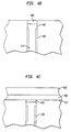
- Fig. 4d shows the process for defining the active area of the DRAM cell.
- the active area is defined using conventional lithographic techniques.
- the non-active region 450 is anisotropically etched by, for example, RIE.
- an anti-reflective layer may be used.
- the non-active region overlaps a portion of the trench, leaving a remaining portion to permit a sufficient amount of current to flow between the transistor and capacitor.
- the non-active region overlaps ⁇ about half the trench width, preferably about half the trench width.
- the non-active region is sufficiently deep to isolate the buried strap from the silicon sidewall opposite the side where the transistor of the DRAM cell is to be formed.
- the non-active region is etched below the top of the oxide collar. In one embodiment, the non-active region is etched about 250 nm below the silicon surface.
- the non-active region is the region where a raised STI is to be formed.
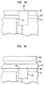
- a dielectric material such as, for example, TEOS is deposited on the surface of the substrate to sufficiently fill the nonactive region 450. Since the TEOS layer is conformal, planarization schemes utilizing, for example, CMP, is performed to planarize the structure. Thereafter, the nitride layer is removed, resulting in the raised STI 455 having a having its top surface planar with the top surface of the poly 482 layer. The removal of the nitride layer may cause a divot 490 to form. However, since the STI is raised, the divot does not extend below the substrate surface. As a result, corner conduction is reduced or eliminated, making V t of the transistors more uniform.
- a poly layer 483 is formed over the poly layer 482.
- the combined thickness of the poly layers is sufficient to formed the gate conductor. In one embodiment, the thickness of the combined layers is about 100 nm.
- a silicide layer 484 comprising refractory metals, such as WSi x to reduce the resistance of the gate conductor, is formed over the poly.
- a nitride layer 484 is formed above the polycide layer or, if no polycide layer is used, above the poly layer 483. The nitride layer serves as an etch stop for boarderless bitline contact etch.
- the surface of the substrate is patterned to form a gate stack for a transistor 470 of the DRAM cell.
- a passing gate stack 480 is typically formed over the trench and isolated therefrom by the raised STI.
- Drain 471 and source 472 are formed by implanting dopants having the appropriate profile to achieve the desired operating characteristics.
- nitride spacers may be employed.
Landscapes
- Engineering & Computer Science (AREA)
- Manufacturing & Machinery (AREA)
- Semiconductor Memories (AREA)
Applications Claiming Priority (2)
| Application Number | Priority Date | Filing Date | Title |
|---|---|---|---|
| US873100 | 1997-06-11 | ||
| US08/873,100 US6100131A (en) | 1997-06-11 | 1997-06-11 | Method of fabricating a random access memory cell |
Publications (2)
| Publication Number | Publication Date |
|---|---|
| EP0884776A2 true EP0884776A2 (fr) | 1998-12-16 |
| EP0884776A3 EP0884776A3 (fr) | 2001-10-17 |
Family
ID=25360971
Family Applications (1)
| Application Number | Title | Priority Date | Filing Date |
|---|---|---|---|
| EP98109820A Withdrawn EP0884776A3 (fr) | 1997-06-11 | 1998-05-29 | Structure isolante pour cellule DRAM avec capacité ensillonée |
Country Status (6)
| Country | Link |
|---|---|
| US (2) | US6100131A (fr) |
| EP (1) | EP0884776A3 (fr) |
| JP (1) | JPH1117152A (fr) |
| KR (1) | KR19990006509A (fr) |
| CN (1) | CN1213167A (fr) |
| TW (1) | TW399293B (fr) |
Cited By (3)
| Publication number | Priority date | Publication date | Assignee | Title |
|---|---|---|---|---|
| WO2001011682A1 (fr) * | 1999-08-09 | 2001-02-15 | Infineon Technologies Ag | Procede permettant de produire une isolation |
| EP0908948A3 (fr) * | 1997-09-23 | 2001-10-24 | Siemens Aktiengesellschaft | Fossé d'isolation peu profond pour capacité ensillonée de type DRAM |
| WO2002041366A3 (fr) * | 2000-11-16 | 2003-04-17 | Infineon Technologies Corp | Implantation d'azote au moyen d'un effet d'ombre pour reguler l'epaisseur de l'oxyde de grille dans des semi-conducteurs dram sti |
Families Citing this family (16)
| Publication number | Priority date | Publication date | Assignee | Title |
|---|---|---|---|---|
| US6037620A (en) * | 1998-06-08 | 2000-03-14 | International Business Machines Corporation | DRAM cell with transfer device extending along perimeter of trench storage capacitor |
| US6794242B1 (en) * | 2000-09-29 | 2004-09-21 | Infineon Technologies Ag | Extendible process for improved top oxide layer for DRAM array and the gate interconnects while providing self-aligned gate contacts |
| US6890859B1 (en) * | 2001-08-10 | 2005-05-10 | Cypress Semiconductor Corporation | Methods of forming semiconductor structures having reduced defects, and articles and devices formed thereby |
| DE10205077B4 (de) * | 2002-02-07 | 2007-03-08 | Infineon Technologies Ag | Halbleiterspeicherzelle mit einem Graben und einem planaren Auswahltransistor und Verfahren zu ihrer Herstellung |
| US6534824B1 (en) * | 2002-02-20 | 2003-03-18 | International Business Machines Corporation | Self-aligned punch through stop for 6F2 rotated hybrid DRAM cell |
| DE10220584B3 (de) * | 2002-05-08 | 2004-01-08 | Infineon Technologies Ag | Dynamische Speicherzelle und Verfahren zum Herstellen derselben |
| US6682982B1 (en) * | 2002-10-03 | 2004-01-27 | Taiwan Semiconductor Manufacturing Company | Process method for 1T-SRAM |
| US6703274B1 (en) * | 2003-01-03 | 2004-03-09 | International Business Machines Corporation | Buried strap with limited outdiffusion and vertical transistor DRAM |
| US6909136B2 (en) * | 2003-07-14 | 2005-06-21 | Nanya Technology Corp. | Trench-capacitor DRAM cell having a folded gate conductor |
| US7273794B2 (en) | 2003-12-11 | 2007-09-25 | International Business Machines Corporation | Shallow trench isolation fill by liquid phase deposition of SiO2 |
| US6887761B1 (en) * | 2004-03-17 | 2005-05-03 | International Business Machines Corporation | Vertical semiconductor devices |
| CN100424856C (zh) * | 2005-07-20 | 2008-10-08 | 联华电子股份有限公司 | 制作沟渠电容动态随机存取存储器元件的方法 |
| US7427545B2 (en) * | 2005-11-21 | 2008-09-23 | International Business Machines Corporation | Trench memory cells with buried isolation collars, and methods of fabricating same |
| US7326986B2 (en) * | 2006-01-06 | 2008-02-05 | International Business Machines Corporation | Trench memory |
| CN105609503A (zh) * | 2016-01-25 | 2016-05-25 | 中国科学院微电子研究所 | 存储单元、存储器件及电子设备 |
| CN109416897B (zh) * | 2016-07-29 | 2021-07-02 | 索尼公司 | 显示装置、显示装置制造方法以及电子设备 |
Family Cites Families (20)
| Publication number | Priority date | Publication date | Assignee | Title |
|---|---|---|---|---|
| JPH07112049B2 (ja) * | 1992-01-09 | 1995-11-29 | インターナショナル・ビジネス・マシーンズ・コーポレイション | ダイナミック・ランダム・アクセス・メモリ・デバイスおよび製造方法 |
| JPH05347390A (ja) * | 1992-06-15 | 1993-12-27 | Toshiba Corp | 半導体記憶装置およびその製造方法 |
| US5422294A (en) * | 1993-05-03 | 1995-06-06 | Noble, Jr.; Wendell P. | Method of making a trench capacitor field shield with sidewall contact |
| US5389559A (en) * | 1993-12-02 | 1995-02-14 | International Business Machines Corporation | Method of forming integrated interconnect for very high density DRAMs |
| US5369049A (en) * | 1993-12-17 | 1994-11-29 | International Business Machines Corporation | DRAM cell having raised source, drain and isolation |
| US5395786A (en) * | 1994-06-30 | 1995-03-07 | International Business Machines Corporation | Method of making a DRAM cell with trench capacitor |
| US5451809A (en) * | 1994-09-07 | 1995-09-19 | Kabushiki Kaisha Toshiba | Smooth surface doped silicon film formation |
| US5627092A (en) * | 1994-09-26 | 1997-05-06 | Siemens Aktiengesellschaft | Deep trench dram process on SOI for low leakage DRAM cell |
| US5521422A (en) * | 1994-12-02 | 1996-05-28 | International Business Machines Corporation | Corner protected shallow trench isolation device |
| US5539229A (en) * | 1994-12-28 | 1996-07-23 | International Business Machines Corporation | MOSFET with raised STI isolation self-aligned to the gate stack |
| US5576566A (en) * | 1995-04-13 | 1996-11-19 | International Business Machines Corporation | Semiconductor trench capacitor cell having a buried strap |
| JP3311205B2 (ja) * | 1995-07-13 | 2002-08-05 | 株式会社東芝 | 半導体記憶装置及びその製造方法 |
| US5614431A (en) * | 1995-12-20 | 1997-03-25 | International Business Machines Corporation | Method of making buried strap trench cell yielding an extended transistor |
| US5827765A (en) * | 1996-02-22 | 1998-10-27 | Siemens Aktiengesellschaft | Buried-strap formation in a dram trench capacitor |
| US5770875A (en) * | 1996-09-16 | 1998-06-23 | International Business Machines Corporation | Large value capacitor for SOI |
| US5874345A (en) * | 1996-11-18 | 1999-02-23 | International Business Machines Corporation | Method for planarizing TEOS SiO2 filled shallow isolation trenches |
| US6037620A (en) * | 1998-06-08 | 2000-03-14 | International Business Machines Corporation | DRAM cell with transfer device extending along perimeter of trench storage capacitor |
| US6140175A (en) * | 1999-03-03 | 2000-10-31 | International Business Machines Corporation | Self-aligned deep trench DRAM array device |
| US6259129B1 (en) * | 1999-04-20 | 2001-07-10 | International Business Machines Corporation | Strap with intrinsically conductive barrier |
| US6153902A (en) * | 1999-08-16 | 2000-11-28 | International Business Machines Corporation | Vertical DRAM cell with wordline self-aligned to storage trench |
-
1997
- 1997-06-11 US US08/873,100 patent/US6100131A/en not_active Expired - Fee Related
-
1998
- 1998-05-21 TW TW087107884A patent/TW399293B/zh not_active IP Right Cessation
- 1998-05-29 KR KR1019980019647A patent/KR19990006509A/ko not_active Withdrawn
- 1998-05-29 EP EP98109820A patent/EP0884776A3/fr not_active Withdrawn
- 1998-06-08 JP JP10159155A patent/JPH1117152A/ja not_active Withdrawn
- 1998-06-09 CN CN98109583A patent/CN1213167A/zh active Pending
-
1999
- 1999-12-01 US US09/452,217 patent/US6399977B1/en not_active Expired - Fee Related
Cited By (6)
| Publication number | Priority date | Publication date | Assignee | Title |
|---|---|---|---|---|
| EP0908948A3 (fr) * | 1997-09-23 | 2001-10-24 | Siemens Aktiengesellschaft | Fossé d'isolation peu profond pour capacité ensillonée de type DRAM |
| WO2001011682A1 (fr) * | 1999-08-09 | 2001-02-15 | Infineon Technologies Ag | Procede permettant de produire une isolation |
| US6638814B1 (en) | 1999-08-09 | 2003-10-28 | Infineon Technologies Aktiengesellschaft | Method for producing an insulation |
| WO2002041366A3 (fr) * | 2000-11-16 | 2003-04-17 | Infineon Technologies Corp | Implantation d'azote au moyen d'un effet d'ombre pour reguler l'epaisseur de l'oxyde de grille dans des semi-conducteurs dram sti |
| US6967147B1 (en) | 2000-11-16 | 2005-11-22 | Infineon Technologies Ag | Nitrogen implantation using a shadow effect to control gate oxide thickness in DRAM semiconductor |
| US7767562B2 (en) | 2000-11-16 | 2010-08-03 | Qimonda Ag | Method of implanting using a shadow effect |
Also Published As
| Publication number | Publication date |
|---|---|
| JPH1117152A (ja) | 1999-01-22 |
| KR19990006509A (ko) | 1999-01-25 |
| TW399293B (en) | 2000-07-21 |
| US6399977B1 (en) | 2002-06-04 |
| US6100131A (en) | 2000-08-08 |
| CN1213167A (zh) | 1999-04-07 |
| EP0884776A3 (fr) | 2001-10-17 |
Similar Documents
| Publication | Publication Date | Title |
|---|---|---|
| US5867420A (en) | Reducing oxidation stress in the fabrication of devices | |
| US6163045A (en) | Reduced parasitic leakage in semiconductor devices | |
| US6008104A (en) | Method of fabricating a trench capacitor with a deposited isolation collar | |
| US5943581A (en) | Method of fabricating a buried reservoir capacitor structure for high-density dynamic random access memory (DRAM) circuits | |
| US6310375B1 (en) | Trench capacitor with isolation collar and corresponding manufacturing method | |
| US6100131A (en) | Method of fabricating a random access memory cell | |
| US5843820A (en) | Method of fabricating a new dynamic random access memory (DRAM) cell having a buried horizontal trench capacitor | |
| US6204112B1 (en) | Process for forming a high density semiconductor device | |
| US6806137B2 (en) | Trench buried bit line memory devices and methods thereof | |
| US6008513A (en) | Dynamic random access memory (DRAM) cells with minimum active cell areas using sidewall-space bit lines | |
| US6437388B1 (en) | Compact trench capacitor memory cell with body contact | |
| US6504210B1 (en) | Fully encapsulated damascene gates for Gigabit DRAMs | |
| US6661049B2 (en) | Microelectronic capacitor structure embedded within microelectronic isolation region | |
| EP0884785B1 (fr) | Cellule DRAM à capacité ensillonée avec transistor vertical | |
| EP0905783B1 (fr) | Transistor vertical pour une cellule mémoire comprenant un condensateur à tranchée | |
| US6946344B2 (en) | Method for forming trench capacitor | |
| JP3877997B2 (ja) | ダイナミックランダムアクセスメモリセルを形成する方法 | |
| US6828615B2 (en) | Vertical internally-connected trench cell (V-ICTC) and formation method for semiconductor memory devices | |
| HK1015532A (en) | Isolation structure for dram cell with trench capacitor | |
| HK1017139A (en) | Shallow trench isolation for dram trench capacitor | |
| HK1015535A (en) | Trench capacitor dram cell with vertical transistor | |
| HK1020111A (en) | A trench capacitor with isolation collar | |
| HK1017146A (en) | Trench capacitor dram cell | |
| HK1022048A (en) | A trench capacitor with isolation collar and corresponding manufacturing method |
Legal Events
| Date | Code | Title | Description |
|---|---|---|---|
| PUAI | Public reference made under article 153(3) epc to a published international application that has entered the european phase |
Free format text: ORIGINAL CODE: 0009012 |
|
| AK | Designated contracting states |
Kind code of ref document: A2 Designated state(s): AT BE CH CY DE DK ES FI FR GB GR IE IT LI LU MC NL PT SE Kind code of ref document: A2 Designated state(s): DE FR GB IE IT NL |
|
| AX | Request for extension of the european patent |
Free format text: AL;LT;LV;MK;RO;SI |
|
| PUAL | Search report despatched |
Free format text: ORIGINAL CODE: 0009013 |
|
| AK | Designated contracting states |
Kind code of ref document: A3 Designated state(s): AT BE CH CY DE DK ES FI FR GB GR IE IT LI LU MC NL PT SE |
|
| AX | Request for extension of the european patent |
Free format text: AL;LT;LV;MK;RO;SI |
|
| 17P | Request for examination filed |
Effective date: 20020122 |
|
| AKX | Designation fees paid |
Free format text: DE FR GB IE IT NL |
|
| STAA | Information on the status of an ep patent application or granted ep patent |
Free format text: STATUS: THE APPLICATION IS DEEMED TO BE WITHDRAWN |
|
| 18D | Application deemed to be withdrawn |
Effective date: 20021203 |
|
| REG | Reference to a national code |
Ref country code: HK Ref legal event code: WD Ref document number: 1015532 Country of ref document: HK |