EP0889508B1 - Procédé pour l'attaque sèche d'une structure d'électrode - Google Patents
Procédé pour l'attaque sèche d'une structure d'électrode Download PDFInfo
- Publication number
- EP0889508B1 EP0889508B1 EP98111994A EP98111994A EP0889508B1 EP 0889508 B1 EP0889508 B1 EP 0889508B1 EP 98111994 A EP98111994 A EP 98111994A EP 98111994 A EP98111994 A EP 98111994A EP 0889508 B1 EP0889508 B1 EP 0889508B1
- Authority
- EP
- European Patent Office
- Prior art keywords
- layer
- etching
- chemical
- electrode arrangement
- conductive
- Prior art date
- Legal status (The legal status is an assumption and is not a legal conclusion. Google has not performed a legal analysis and makes no representation as to the accuracy of the status listed.)
- Expired - Lifetime
Links
Images


Classifications
-
- H—ELECTRICITY
- H10—SEMICONDUCTOR DEVICES; ELECTRIC SOLID-STATE DEVICES NOT OTHERWISE PROVIDED FOR
- H10D—INORGANIC ELECTRIC SEMICONDUCTOR DEVICES
- H10D84/00—Integrated devices formed in or on semiconductor substrates that comprise only semiconducting layers, e.g. on Si wafers or on GaAs-on-Si wafers
- H10D84/01—Manufacture or treatment
- H10D84/02—Manufacture or treatment characterised by using material-based technologies
- H10D84/03—Manufacture or treatment characterised by using material-based technologies using Group IV technology, e.g. silicon technology or silicon-carbide [SiC] technology
- H10D84/038—Manufacture or treatment characterised by using material-based technologies using Group IV technology, e.g. silicon technology or silicon-carbide [SiC] technology using silicon technology, e.g. SiGe
-
- H—ELECTRICITY
- H10—SEMICONDUCTOR DEVICES; ELECTRIC SOLID-STATE DEVICES NOT OTHERWISE PROVIDED FOR
- H10D—INORGANIC ELECTRIC SEMICONDUCTOR DEVICES
- H10D1/00—Resistors, capacitors or inductors
- H10D1/60—Capacitors
- H10D1/68—Capacitors having no potential barriers
- H10D1/692—Electrodes
-
- H—ELECTRICITY
- H10—SEMICONDUCTOR DEVICES; ELECTRIC SOLID-STATE DEVICES NOT OTHERWISE PROVIDED FOR
- H10P—GENERIC PROCESSES OR APPARATUS FOR THE MANUFACTURE OR TREATMENT OF DEVICES COVERED BY CLASS H10
- H10P50/00—Etching of wafers, substrates or parts of devices
- H10P50/20—Dry etching; Plasma etching; Reactive-ion etching
- H10P50/26—Dry etching; Plasma etching; Reactive-ion etching of conductive or resistive materials
- H10P50/264—Dry etching; Plasma etching; Reactive-ion etching of conductive or resistive materials by chemical means
- H10P50/266—Dry etching; Plasma etching; Reactive-ion etching of conductive or resistive materials by chemical means by vapour etching only
- H10P50/267—Dry etching; Plasma etching; Reactive-ion etching of conductive or resistive materials by chemical means by vapour etching only using plasmas
-
- H—ELECTRICITY
- H10—SEMICONDUCTOR DEVICES; ELECTRIC SOLID-STATE DEVICES NOT OTHERWISE PROVIDED FOR
- H10P—GENERIC PROCESSES OR APPARATUS FOR THE MANUFACTURE OR TREATMENT OF DEVICES COVERED BY CLASS H10
- H10P50/00—Etching of wafers, substrates or parts of devices
- H10P50/71—Etching of wafers, substrates or parts of devices using masks for conductive or resistive materials
Definitions
- barium strontium titanate BST, (Ba, Sr) TiO 3
- lead zirconium titanate PZT, Pb (Zr, Ti) O 3
- lanthanum-doped lead zirconium titanate or strontium bismuth tantalate SBT, SrBi 2 Ta 2 O 9
- Electrodes bottom electrodes
- the processing takes place at high temperatures so that the materials which usually make up the capacitor electrodes exist, e.g. doped polysilicon, slightly oxidized and lose their electrically conductive properties, which would lead to the failure of the memory cell.
- the materials used so far are structured usually through so-called plasma-assisted anisotropic Etching process.
- plasma-assisted anisotropic Etching process Usually physical-chemical Process used in which gas mixtures from a or several reactive gases, e.g. Oxygen, Chlorine, bromine, hydrogen chloride, hydrogen bromide or halogenated Hydrocarbons and noble gases (e.g. Ar, He) be used.
- gases e.g. Oxygen, Chlorine, bromine, hydrogen chloride, hydrogen bromide or halogenated Hydrocarbons and noble gases (e.g. Ar, He) be used.
- These gas mixtures are usually in an alternating electromagnetic field at low pressures excited (US 5,515,984).
- FIG. 7 shows the basic mode of operation of an etching chamber, illustrated using the example of a parallel plate reactor 20.
- the gas mixture for example Ar and Cl 2
- the gas mixture is fed to the actual reactor chamber 22 via the gas inlet 21 and pumped out again through the gas outlet 29.
- the lower plate 24 of the parallel plate reactor is connected to a high-frequency source 28 via a capacitor 27 and serves as a substrate holder.
- the gas mixture is converted into a plasma 25. Since the mobility of the electrons is greater than that of the gas cations, the upper and lower plates 23, 24 charge negatively with respect to the plasma 25.
- both plates 23, 24 exert a high attraction on the positively charged gas cations, so that they are exposed to permanent bombardment by these ions, for example Ar + .
- the gas pressure is also kept low, typically 0.1-10 Pa, there is only a slight scattering of the ions among one another and on the neutral particles, and the ions hit almost perpendicularly on the surface of a substrate 26 which is held on the lower plate 24 of the parallel plate reactor is. This allows a mask (not shown) to be imaged well on the underlying layer of the substrate 26 to be etched.
- Photoresists are usually used as mask materials, since this involves an exposure step and a development step can be structured relatively easily.
- the physical part of the etching is caused by momentum and kinetic energy of the impinging ions (eg Cl 2 + , Ar + ).
- chemical reactions between the substrate and the reactive gas particles ions, molecules, atoms, radicals
- ions, molecules, atoms, radicals are initiated or intensified to form volatile reaction products (chemical part of the etching).
- the etching removal of the layer to be structured the same order of magnitude as the etching removal of the mask or Underlay (etch stop layer), i.e. the etch selectivity for Etching mask or underlay is generally small (between about 0.3 and 3.0).
- the selectivity of the etching is therefore described in US Pat. No. 5,350,705 the use of a titanium hard mask removed after the etching proposed.
- a chemical dry etching is said to be a common practice dry chemical etching using, possibly excited, halogens, hydrogen halides or halogenated Hydrocarbons or using oxygen can be understood at usual temperatures and gas pressures. It is also said to be under a material that is chemical Dry etching is practically not etchable, a material is understood be the optimum for the respective material Process conditions has an etching rate of less than 1 nm / min. Accordingly, under a low etching rate Etching rate greater than 1 nm / min for the respective material optimal process conditions can be understood.
- the material of the first layer is dry chemical etched is practically not etchable, the first layer during a normal chemical-physical dry etching mainly through the physical part of the chemical-physical Dry etching removed. In contrast to becomes the second layer during a usual chemical-physical Dry etching also through the chemical part the chemical-physical dry etching.
- the invention has the advantage that the effective thickness the electrode arrangement is increased by the height of the second layer, so that a breakdown during overetching at a Contacting the electrode arrangement is avoided. As well is the formation of difficult-to-remove speech positions from the material of the first layer during the overetch prevented.
- the second layer reduces the electrode arrangement - with approximately constant capacity - the Sheet resistance of the electrode arrangement. This will make it Switching the so-called “common plate” in the so-called “pulsed-plateline” operation of the memory cell accelerates, which shortens the access time of the entire block.
- the second layer enables the electrode arrangement an encapsulation of the capacitor of the memory cell with an oxide layer.
- the first layer preferably contains a 4d or 5d transition metal, their conductive nitrides or their conductive oxides
- the first layer contains ruthenium, rhodium, Palladium, osmium, iridium, platinum, gold, silver or rhenium.
- the second layer is aluminum, Titanium, tungsten, their conductive silicides, their conductive Contains nitrides or their conductive oxides.
- the second layer contains titanium or a titanium nitride, in particular TiN x 0.8 ⁇ x ⁇ 1.2.
- the invention has the further advantage that the metals, metal silicides, Metal nitrides or metal oxides of the second Layer are more resistant compared to photoresists, so that chemical "ashing" of the mask is prevented.
- the high binding energy of the metal atoms in metals or Metal ions in silicides, nitrides or oxides leads to a lot low removal rates in etching processes with a high physical Proportion of. Overall, this has the consequence that the selectivity the etching process of the first layer is increased.
- the lower mask erosion results in a higher one Dimensional accuracy of the structuring. Beyond that by the method according to the invention also with reactive gases achieve steeper etching edges on the layer to be structured.
- a plasma etching method is preferred for dry etching of the second layer used.
- the first layer at least one reactive substance, in particular a reactive gas is provided which is compatible with the material the second layer on the surface of the second layer of a non-volatile connection.
- a reactive gas is provided which is compatible with the material the second layer on the surface of the second layer of a non-volatile connection.
- the reactive gas is selected from a group consisting of the gases oxygen (O 2 ), nitrogen (N 2 ), hydrogen (H 2 ), halogens, gaseous halogen compounds or a mixture of these gases.
- an inert gas preferably argon, is provided in the first layer is.
- the first is advantageously used for dry etching Layer a reactive ion etching (RIE, Reactive Ion Etching), a magnetic field assisted reactive ion etching (MERIE, Magnetically Enhanced RIE), an ECR etching (ECR, Electron Cyclotron Resonance) or inductively coupled plasma etching (ICP, TCP) used.
- RIE reactive ion etching
- MIE magnetic field assisted reactive ion etching
- ECR Electron Cyclotron Resonance
- ICP inductively coupled plasma etching
- the insulation layer is a silicon oxide layer is or contains.
- the silicon oxide layer is generated by a TEOS or a silane process.
- an aluminum, Tungsten or copper layer used.
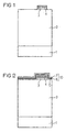
- FIGS 1 to 3 show a schematic representation of the inventive method.
- oxide is deposited several times as part of normal process control, so that finally an oxide layer up to 2 ⁇ m thick 2 is generated.
- Titanium layer 3 serves as a barrier material for the following platinum layer 4.
- the platinum layer 4 serves in the following as a bottom electrode for the capacitor of a memory cell and is therefore with a contact (not shown) Mistake.
- the platinum layer 4 can be sputtered, for example be applied.
- Below is the platinum layer 4 and the titanium layer 3 structured. This structuring the platinum layer 4 can be analogous to by means of a TiN hard mask the structuring of the top electrode described below respectively. However, with the platinum layer 4 (bottom electrode) the TiN hard mask again after structuring away.
- the resulting structure is in Fig. 1 shown.
- a barium strontium titanate layer 5 (BST, (Ba, Sr) TiO 3 ) is then applied to the structure shown in FIG. 1. This layer is later used in the complete memory cell as the dielectric of the storage capacitor.
- a further platinum layer 6 is applied to the barium strontium titanate layer 5 as the first conductive layer of the electrode arrangement according to the invention.
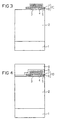
- a titanium nitride layer 7 is subsequently produced on the platinum layer 6 as the second conductive layer of the electrode arrangement 10 according to the invention. The resulting structure is shown in Fig. 2.
- the titanium nitride layer 7 is now by means of a photo technique structured to act as a "hard mask” for structuring the platinum layer 6 and the barium strontium titanate layer 5 serve to be able to.
- RIE reactive ion etching
- Oxygen O 2 or a mixture of O 2 and other gases, for example argon is used as the etching gas.
- RIE reactive ion etching
- other dry etching processes such as ion etching, magnetic field-assisted reactive ion etching (MERIE, Magnetically Enhanced RIE), ECR etching (ECR, Electron Cyclotron Resonance) or inductively coupled plasma etching processes (ICP, TCP) can be used.
- non-volatile titanium oxide layers (Ti x O y ) are continuously simulated on the surface of the titanium nitride mask 7, as a result of which the etching rate of the titanium nitride mask 7 is reduced even further. Accordingly, the selectivity of the etching process is significantly increased.
- the associated lower mask erosion results in a higher dimensional accuracy of the structuring.
- the flank angle of the etching flank on the platinum layer 6 can be set over a wide range by a suitable choice of the O 2 concentration. In this way, the electrode arrangement according to the invention can be manufactured with high dimensional accuracy.
- the corresponding areas of the barium strontium titanate layer 5 are subjected to the reactive ion etching.
- oxygen O 2 or a mixture of O 2 and other gases, for example argon, is used as the etching gas in order to further "harden" the titanium nitride hard mask 7.
- the method 10 according to the invention has the advantage that through the titanium nitride layer 7 (second layer of the electrode arrangement), with approximately constant capacity, the Sheet resistance of the entire electrode arrangement 10 is reduced. This switches the so-called “common plate” in the so-called “pulsed-plateline” operation of the memory cell accelerates, which increases the access time of the whole Building block shortened.
- a thin SiO 2 layer 8 is applied to the entire surface of the structure shown in FIG. 3, for example by a TEOS process. Since the deposition of an oxide layer on platinum is problematic, the titanium nitride layer 7 (second layer of the electrode arrangement) enables the capacitor of the memory cell to be encapsulated with an oxide layer. Then a lacquer layer 9 is applied to the thin SiO 2 layer 8. The resulting structure is shown in Fig. 4.
- a plasma etching process is subsequently carried out in order to To produce contact holes 12 and 13. Because of the different Depth of contact holes 12 and 13 is the electrode arrangement 10 exposed to a long overetch.
- the electrode assembly 10 has through the titanium nitride layer 7 (second layer of the electrode arrangement) greater thickness, so that a break through the electrode arrangement 10 is avoided during contact hole etching.
Landscapes
- Semiconductor Memories (AREA)
- Drying Of Semiconductors (AREA)
- Electrodes Of Semiconductors (AREA)
- Semiconductor Integrated Circuits (AREA)
- Junction Field-Effect Transistors (AREA)
Claims (11)
- Procédé de production d'une structure (10) d'électrode comprenant les stades :on dispose une première couche (6) conductrice de la structure (10) d'électrode , la matière de la première couche (6) ne pouvant pratiquement pas être attaquée par une attaque chimique par voie sèche,on dispose une deuxième couche (7) conductrice de la structure (10) d'électrode sur la première couche (6), la matière de la deuxième couche (7) pouvant être attaquée par une attaque chimique par voie sèche à une petite vitesse d'attaque,on structure la deuxième couche (7) par une attaque chemio-physique par voie sèche, la deuxième couche (7) étant, pendant l'attaque chemio-physique par voie sèche, enlevée aussi par la partie chimique de l'attaque chemio-physique par voie sèche,on attaque chemio-physiquement par voie sèche la première couche (6) de la structure (10) d'électrode en utilisant la deuxième couche (7) structurée comme masque, la première couche (6) étant enlevée pendant l'attaque chemio-physique par voie sèche principalement par la partie physique de l'attaque chemio-physique par voie sèche,on dépose et on structure sur la structure (10) d'électrode au moins une couche (9) d'isolement, de manière à former au moins un trou (12) métallisé par rapport à la structure (10) d'électrode et un autre trou (13) métallisé disposé à l'extérieur de la structure d'électrode, de sorte que, par une différence de profondeur des trous (12, 13) métallisés, la structure (10) d'électrode soit soumise à une attaque excessive longue dans laquelle, pendant l'attaque des trous métallisés, il est évité que la structure (10) d'électrode ne soit percée en raison de l'épaisseur plus grande que la structure (10) d'électrode possède par la deuxième couche (7) eton dépose une couche conductrice de manière à combler les trous (12, 13) métallisés.
- Procédé suivant la revendication 1, caractérisé en ce que la première couche (6) contient un métal de transition 4d ou 5d, leurs nitrures conducteurs ou leurs oxydes conducteurs.
- Procédé suivant la revendication 1 ou 2, caractérisé en ce que la deuxième couche (7) contient de l'aluminium, du titane, du tungstène, leurs siliciures conducteurs, leurs nitrures conducteurs ou leurs oxydes conducteurs.
- Procédé suivant l'une des revendications 1 à 3, caractérisé en ce que la première couche (6) contient du ruthénium, du rhodium, du palladium, de l'osmium, de l'iridium, du platine, de l'or, de l'argent ou du rhénium.
- Procédé suivant l'une des revendications 1 à 4, caractérisé en ce que la deuxième couche (7) contient du titane ou un nitrure de titane, notamment TiNx 0,8 < x < 1,2.
- Procédé suivant l'une des revendications précédentes, caractérisé en ce que l'on utilise pour l'attaque par voie sèche de la deuxième couche (7) un procédé d'attaque au plasma.
- Procédé suivant l'une des revendications précédentes, caractérisé en ce qu'il est prévu pendant l'attaque par voie sèche de la première couche (6) au moins un gaz réactif qui réagit sur la matière de la deuxième couche (7) à la surface de la deuxième couche (7) pour donner un composé non volatil,
et en ce que le gaz réactif est de l'oxygène (O2), de l'azote (N2), de l'hydrogène (H2), un halogène, un composé halogéné gazeux ou un mélange de ces gaz ou un gaz rare. - Procédé suivant l'une des revendications précédentes, caractérisé en ce que pour l'attaque par voie sèche de la première couche (6) on met en oeuvre une attaque réactive ionique (RIE, Reactive Ion Etching), une attaque réactive ionique exaltée par champ magnétique (MERIE, Magnetically Enhanced RIE), ou une attaque ECR (ECR, Electron Cyclotron Resonance) ou un procédé d'attaque au plasma à couplage inductif (ICP, TCP).
- Procédé suivant l'une des revendications précédentes, caractérisé en ce que la couche (8) d'isolement est une couche d'oxyde de silicium ou contient une couche d'oxyde de silicium.
- Procédé suivant la revendication 9, caractérisé en ce que la couche (8) d'oxyde de silicium est produite par une opération au TEOS ou au silane.
- Procédé suivant l'une des revendications précédentes, caractérisé en ce que l'on utilise comme couche conductrice une couche d'aluminium, une couche de tungstène ou une couche cuivre.
Applications Claiming Priority (2)
| Application Number | Priority Date | Filing Date | Title |
|---|---|---|---|
| DE19728474A DE19728474A1 (de) | 1997-07-03 | 1997-07-03 | Elektrodenanordnung |
| DE19728474 | 1997-07-03 |
Publications (3)
| Publication Number | Publication Date |
|---|---|
| EP0889508A2 EP0889508A2 (fr) | 1999-01-07 |
| EP0889508A3 EP0889508A3 (fr) | 1999-06-02 |
| EP0889508B1 true EP0889508B1 (fr) | 2002-05-08 |
Family
ID=7834561
Family Applications (1)
| Application Number | Title | Priority Date | Filing Date |
|---|---|---|---|
| EP98111994A Expired - Lifetime EP0889508B1 (fr) | 1997-07-03 | 1998-06-29 | Procédé pour l'attaque sèche d'une structure d'électrode |
Country Status (7)
| Country | Link |
|---|---|
| US (1) | US7045070B1 (fr) |
| EP (1) | EP0889508B1 (fr) |
| JP (1) | JPH11233725A (fr) |
| KR (1) | KR100446580B1 (fr) |
| CN (1) | CN1146960C (fr) |
| DE (2) | DE19728474A1 (fr) |
| TW (1) | TW414954B (fr) |
Families Citing this family (8)
| Publication number | Priority date | Publication date | Assignee | Title |
|---|---|---|---|---|
| DE19901002B4 (de) * | 1999-01-13 | 2005-09-22 | Infineon Technologies Ag | Verfahren zum Strukturieren einer Schicht |
| DE19935131B4 (de) * | 1999-07-27 | 2006-01-26 | Infineon Technologies Ag | Verfahren zur Beseitigung von Redepositionen von einem Wafer |
| DE10004391C2 (de) * | 2000-02-02 | 2002-05-16 | Infineon Technologies Ag | Verfahren zur Durchführung eines Plasmaätzprozesses |
| TWI326908B (en) | 2006-09-11 | 2010-07-01 | Ind Tech Res Inst | Packaging structure and fabricating method thereof |
| US8986921B2 (en) | 2013-01-15 | 2015-03-24 | International Business Machines Corporation | Lithographic material stack including a metal-compound hard mask |
| US8987133B2 (en) | 2013-01-15 | 2015-03-24 | International Business Machines Corporation | Titanium oxynitride hard mask for lithographic patterning |
| US8853095B1 (en) | 2013-05-30 | 2014-10-07 | International Business Machines Corporation | Hybrid hard mask for damascene and dual damascene |
| JP2015133424A (ja) * | 2014-01-14 | 2015-07-23 | 住友電工デバイス・イノベーション株式会社 | 電子部品の製造方法 |
Family Cites Families (22)
| Publication number | Priority date | Publication date | Assignee | Title |
|---|---|---|---|---|
| JPS6320079A (ja) * | 1986-07-11 | 1988-01-27 | ヤンマー農機株式会社 | 穀粒などの粒状体の感知センサ−装置 |
| US5057455A (en) * | 1989-11-30 | 1991-10-15 | At&T Bell Laboratories | Formation of integrated circuit electrodes |
| US5122225A (en) * | 1990-11-21 | 1992-06-16 | Texas Instruments Incorporated | Selective etch method |
| US5208170A (en) * | 1991-09-18 | 1993-05-04 | International Business Machines Corporation | Method for fabricating bipolar and CMOS devices in integrated circuits using contact metallization for local interconnect and via landing |
| US5269880A (en) * | 1992-04-03 | 1993-12-14 | Northern Telecom Limited | Tapering sidewalls of via holes |
| JP3086747B2 (ja) * | 1992-05-07 | 2000-09-11 | 三菱電機株式会社 | 半導体装置およびその製造方法 |
| US5350705A (en) * | 1992-08-25 | 1994-09-27 | National Semiconductor Corporation | Ferroelectric memory cell arrangement having a split capacitor plate structure |
| KR960005246B1 (ko) * | 1992-10-21 | 1996-04-23 | 현대전자산업주식회사 | 캐패시터의 저장전극 제조방법 |
| US5341016A (en) * | 1993-06-16 | 1994-08-23 | Micron Semiconductor, Inc. | Low resistance device element and interconnection structure |
| US5562801A (en) * | 1994-04-28 | 1996-10-08 | Cypress Semiconductor Corporation | Method of etching an oxide layer |
| KR0132831B1 (ko) * | 1994-07-08 | 1998-04-16 | 김광호 | 매몰 비트라인과 핀구조 커패시터를 갖는 반도체장치 셀 제조방법 |
| JP3122579B2 (ja) * | 1994-07-27 | 2001-01-09 | シャープ株式会社 | Pt膜のエッチング方法 |
| US5566045A (en) * | 1994-08-01 | 1996-10-15 | Texas Instruments, Inc. | High-dielectric-constant material electrodes comprising thin platinum layers |
| US5585300A (en) * | 1994-08-01 | 1996-12-17 | Texas Instruments Incorporated | Method of making conductive amorphous-nitride barrier layer for high-dielectric-constant material electrodes |
| US5436190A (en) * | 1994-11-23 | 1995-07-25 | United Microelectronics Corporation | Method for fabricating semiconductor device isolation using double oxide spacers |
| KR0168346B1 (ko) * | 1994-12-29 | 1998-12-15 | 김광호 | 고유전율 재료를 이용한 커패시터 및 그 제조방법 |
| US5621906A (en) * | 1995-02-13 | 1997-04-15 | The Trustees Of Columbia University In The City Of New York | Perspective-based interface using an extended masthead |
| US5883781A (en) | 1995-04-19 | 1999-03-16 | Nec Corporation | Highly-integrated thin film capacitor with high dielectric constant layer |
| JPH08316430A (ja) | 1995-05-15 | 1996-11-29 | Mitsubishi Electric Corp | 半導体メモリとその製造方法、スタックドキャパシタ |
| US5930639A (en) * | 1996-04-08 | 1999-07-27 | Micron Technology, Inc. | Method for precision etching of platinum electrodes |
| KR100378345B1 (ko) * | 1996-04-17 | 2003-06-12 | 삼성전자주식회사 | 백금 박막의 건식 식각 방법 |
| TW365691B (en) * | 1997-02-05 | 1999-08-01 | Samsung Electronics Co Ltd | Method for etching Pt film of semiconductor device |
-
1997
- 1997-07-03 DE DE19728474A patent/DE19728474A1/de not_active Ceased
-
1998
- 1998-06-10 TW TW087109246A patent/TW414954B/zh not_active IP Right Cessation
- 1998-06-29 EP EP98111994A patent/EP0889508B1/fr not_active Expired - Lifetime
- 1998-06-29 DE DE59804023T patent/DE59804023D1/de not_active Expired - Fee Related
- 1998-07-01 KR KR10-1998-0026348A patent/KR100446580B1/ko not_active Expired - Fee Related
- 1998-07-03 CN CNB981156622A patent/CN1146960C/zh not_active Expired - Fee Related
- 1998-07-03 JP JP10204409A patent/JPH11233725A/ja active Pending
-
2000
- 2000-08-24 US US09/645,807 patent/US7045070B1/en not_active Expired - Fee Related
Also Published As
| Publication number | Publication date |
|---|---|
| DE19728474A1 (de) | 1999-01-07 |
| JPH11233725A (ja) | 1999-08-27 |
| CN1146960C (zh) | 2004-04-21 |
| EP0889508A2 (fr) | 1999-01-07 |
| DE59804023D1 (de) | 2002-06-13 |
| EP0889508A3 (fr) | 1999-06-02 |
| KR100446580B1 (ko) | 2004-11-16 |
| CN1204861A (zh) | 1999-01-13 |
| US7045070B1 (en) | 2006-05-16 |
| TW414954B (en) | 2000-12-11 |
| KR19990013499A (ko) | 1999-02-25 |
Similar Documents
| Publication | Publication Date | Title |
|---|---|---|
| DE19625883C2 (de) | Kondensatorstruktur eines Halbleiterbauteils und Verfahren zum Herstellen derselben | |
| DE69025300T2 (de) | Integrierte Schaltung mit einer planarisierten dielektrischen Schicht | |
| EP0895278A2 (fr) | Procédé de structuration | |
| DE10014315B4 (de) | Verfahren zum Herstellen eines Halbleiterspeichers | |
| DE69626562T2 (de) | Verfahren zum isotropen Ätzen von Silizium, das hochselektiv gegenüber Wolfram ist | |
| DE69837301T2 (de) | Methode, einen Platinfilm in einer Halbleiteranordnung zu ätzen | |
| DE19733391C2 (de) | Strukturierungsverfahren | |
| DE69622261T2 (de) | Verfahren zur herstellung einer struktur unter verwendung von wiederablagerung | |
| DE19728473A1 (de) | Strukturierungsverfahren | |
| EP0889508B1 (fr) | Procédé pour l'attaque sèche d'une structure d'électrode | |
| EP0907203A2 (fr) | Méthode de structuration | |
| EP0889506A2 (fr) | Procédé de gravure | |
| EP0902461A2 (fr) | Procédé de formation de structures à haut facteur de forme | |
| EP1277230B1 (fr) | Procede de fabrication de structures de condensateur | |
| EP1307906A1 (fr) | Structuration de couches ferroelectriques | |
| DE112004000192T5 (de) | Hartmaske mit hoher Selektivität für IR-Sperrschichten zur Herstellung eines ferroelektrischen Kondensators | |
| DE19929307C1 (de) | Verfahren zur Herstellung einer strukturierten Schicht und dadurch hergestellte Elektrode | |
| DE10121657A1 (de) | Mikroelektronische Struktur mit einer Wasserstoffbarrierenschicht | |
| DE10057444A1 (de) | Verfahren zum Herstellen einer Kondensatoranordnung | |
| DE112004001585T5 (de) | Zaunfreies Ätzen einer Iridium-Barriere mit einem steilen Böschungswinkel | |
| DE19620833A1 (de) | Verfahren zur Herstellung eines Kondensators einer Halbleitereinrichtung | |
| DE19906814A1 (de) | Verfahren zur Entfernung von Material von einer Oberfläche | |
| EP0984490A1 (fr) | Procédé de fabrication des couches des materiels structurées | |
| DE10022656B4 (de) | Verfahren zum Entfernen von Strukturen | |
| DE19929306A1 (de) | Verfahren zur Herstellung einer strukturierten Edelmetallschicht |
Legal Events
| Date | Code | Title | Description |
|---|---|---|---|
| PUAI | Public reference made under article 153(3) epc to a published international application that has entered the european phase |
Free format text: ORIGINAL CODE: 0009012 |
|
| AK | Designated contracting states |
Kind code of ref document: A2 Designated state(s): DE FR GB IE IT |
|
| AX | Request for extension of the european patent |
Free format text: AL;LT;LV;MK;RO;SI |
|
| PUAL | Search report despatched |
Free format text: ORIGINAL CODE: 0009013 |
|
| AK | Designated contracting states |
Kind code of ref document: A3 Designated state(s): AT BE CH CY DE DK ES FI FR GB GR IE IT LI LU MC NL PT SE |
|
| AX | Request for extension of the european patent |
Free format text: AL;LT;LV;MK;RO;SI |
|
| 17P | Request for examination filed |
Effective date: 19990805 |
|
| AKX | Designation fees paid |
Free format text: DE FR GB IE IT |
|
| 17Q | First examination report despatched |
Effective date: 20000114 |
|
| RAP1 | Party data changed (applicant data changed or rights of an application transferred) |
Owner name: INFINEON TECHNOLOGIES AG |
|
| RTI1 | Title (correction) |
Free format text: PROCESS FOR THE DRY ETCHING OF AN ELECTRODE STRUCTURE |
|
| GRAG | Despatch of communication of intention to grant |
Free format text: ORIGINAL CODE: EPIDOS AGRA |
|
| RTI1 | Title (correction) |
Free format text: PROCESS FOR THE DRY ETCHING OF AN ELECTRODE STRUCTURE |
|
| GRAG | Despatch of communication of intention to grant |
Free format text: ORIGINAL CODE: EPIDOS AGRA |
|
| GRAG | Despatch of communication of intention to grant |
Free format text: ORIGINAL CODE: EPIDOS AGRA |
|
| GRAH | Despatch of communication of intention to grant a patent |
Free format text: ORIGINAL CODE: EPIDOS IGRA |
|
| REG | Reference to a national code |
Ref country code: GB Ref legal event code: IF02 |
|
| GRAH | Despatch of communication of intention to grant a patent |
Free format text: ORIGINAL CODE: EPIDOS IGRA |
|
| GRAA | (expected) grant |
Free format text: ORIGINAL CODE: 0009210 |
|
| AK | Designated contracting states |
Kind code of ref document: B1 Designated state(s): DE FR GB IE IT |
|
| REG | Reference to a national code |
Ref country code: IE Ref legal event code: FG4D Free format text: GERMAN |
|
| REF | Corresponds to: |
Ref document number: 59804023 Country of ref document: DE Date of ref document: 20020613 |
|
| GBT | Gb: translation of ep patent filed (gb section 77(6)(a)/1977) |
Effective date: 20020721 |
|
| ET | Fr: translation filed | ||
| PLBE | No opposition filed within time limit |
Free format text: ORIGINAL CODE: 0009261 |
|
| STAA | Information on the status of an ep patent application or granted ep patent |
Free format text: STATUS: NO OPPOSITION FILED WITHIN TIME LIMIT |
|
| 26N | No opposition filed |
Effective date: 20030211 |
|
| REG | Reference to a national code |
Ref country code: GB Ref legal event code: 727 |
|
| REG | Reference to a national code |
Ref country code: GB Ref legal event code: 727J |
|
| REG | Reference to a national code |
Ref country code: GB Ref legal event code: 711B |
|
| REG | Reference to a national code |
Ref country code: GB Ref legal event code: 711G |
|
| REG | Reference to a national code |
Ref country code: GB Ref legal event code: 711A Free format text: TRANSLATIONS FILED: PATENT NO. EP0889508 ON 20040901 |
|
| PGFP | Annual fee paid to national office [announced via postgrant information from national office to epo] |
Ref country code: GB Payment date: 20060615 Year of fee payment: 9 |
|
| GBPC | Gb: european patent ceased through non-payment of renewal fee |
Effective date: 20070629 |
|
| PG25 | Lapsed in a contracting state [announced via postgrant information from national office to epo] |
Ref country code: GB Free format text: LAPSE BECAUSE OF NON-PAYMENT OF DUE FEES Effective date: 20070629 |
|
| PGFP | Annual fee paid to national office [announced via postgrant information from national office to epo] |
Ref country code: IT Payment date: 20080624 Year of fee payment: 11 |
|
| PGFP | Annual fee paid to national office [announced via postgrant information from national office to epo] |
Ref country code: IE Payment date: 20080619 Year of fee payment: 11 Ref country code: DE Payment date: 20080812 Year of fee payment: 11 |
|
| PGFP | Annual fee paid to national office [announced via postgrant information from national office to epo] |
Ref country code: FR Payment date: 20080613 Year of fee payment: 11 |
|
| REG | Reference to a national code |
Ref country code: FR Ref legal event code: ST Effective date: 20100226 |
|
| REG | Reference to a national code |
Ref country code: IE Ref legal event code: MM4A |
|
| PG25 | Lapsed in a contracting state [announced via postgrant information from national office to epo] |
Ref country code: IE Free format text: LAPSE BECAUSE OF NON-PAYMENT OF DUE FEES Effective date: 20090629 Ref country code: FR Free format text: LAPSE BECAUSE OF NON-PAYMENT OF DUE FEES Effective date: 20090630 |
|
| PG25 | Lapsed in a contracting state [announced via postgrant information from national office to epo] |
Ref country code: DE Free format text: LAPSE BECAUSE OF NON-PAYMENT OF DUE FEES Effective date: 20100101 |
|
| PG25 | Lapsed in a contracting state [announced via postgrant information from national office to epo] |
Ref country code: IT Free format text: LAPSE BECAUSE OF NON-PAYMENT OF DUE FEES Effective date: 20090629 |