EP0889596A2 - Verfahren und Gerät zur Kalibrierung integrierter Analog-Digital-Wandler - Google Patents
Verfahren und Gerät zur Kalibrierung integrierter Analog-Digital-Wandler Download PDFInfo
- Publication number
- EP0889596A2 EP0889596A2 EP98110847A EP98110847A EP0889596A2 EP 0889596 A2 EP0889596 A2 EP 0889596A2 EP 98110847 A EP98110847 A EP 98110847A EP 98110847 A EP98110847 A EP 98110847A EP 0889596 A2 EP0889596 A2 EP 0889596A2
- Authority
- EP
- European Patent Office
- Prior art keywords
- adc
- calibrating
- measurements
- equation
- merit
- Prior art date
- Legal status (The legal status is an assumption and is not a legal conclusion. Google has not performed a legal analysis and makes no representation as to the accuracy of the status listed.)
- Withdrawn
Links
Images


Classifications
-
- H—ELECTRICITY
- H03—ELECTRONIC CIRCUITRY
- H03M—CODING; DECODING; CODE CONVERSION IN GENERAL
- H03M1/00—Analogue/digital conversion; Digital/analogue conversion
- H03M1/10—Calibration or testing
- H03M1/1009—Calibration
- H03M1/1033—Calibration over the full range of the converter, e.g. for correcting differential non-linearity
-
- H—ELECTRICITY
- H03—ELECTRONIC CIRCUITRY
- H03M—CODING; DECODING; CODE CONVERSION IN GENERAL
- H03M1/00—Analogue/digital conversion; Digital/analogue conversion
- H03M1/12—Analogue/digital converters
-
- H—ELECTRICITY
- H03—ELECTRONIC CIRCUITRY
- H03M—CODING; DECODING; CODE CONVERSION IN GENERAL
- H03M1/00—Analogue/digital conversion; Digital/analogue conversion
- H03M1/66—Digital/analogue converters
Definitions
- the present invention relates to the field of electronics, and, more particularly, to a calibration method and apparatus for analog-to-digital converter circuits.
- Analog-to-digital converters are widely used to process electrical signals in many electronic applications.
- An integrated circuit analog-to-digital converter typically accepts an analog input voltage signal and converts the signal into a digital form as the output.
- a modem digital communication system such as for a cellular telephone base station, for example, may often require an ADC with a high resolution of greater than 12 bits, a bandwidth greater than 200 MHz, and low power consumption and low distortion for improved overall system performance.
- a pipelined ADC includes a series of subconverter stages with each stage including a flash analog-to-digital converter, a digital-to-analog converter (DAC) and an interstage amplifier connecting the DAC to an adjacent stage.
- the last stage typically includes only a flash ADC.
- a multi-step ADC may include one or more similar subconverter stages which are sequentially reused in generating the digital output signal.
- error sources in the subconverter stages of an integrated circuit analog-to-digital converter include offset, noise, DAC and flash ADC errors, and errors in the interstage gain amplifier.
- the subconverter flash ADC error may be readily corrected, for example, by the use of digital error correction logic circuits.
- the kT/C thermal noise error source caused in a sampled-data system may be reduced by proper choice of the sampling capacitor size.
- U.S. Patent No. 4,354,177 discloses an apparatus and method for exciting the input of an ADC with exponential signals to generate histograms to determine an amplitude probability distribution of each digital output value.
- the histograms may be processed in a manner which produces the transfer characteristic of the converter under test which is independent of the dynamic characteristics of the excitation signals, thus eliminating the need for accurate knowledge of the parameter values of the testing circuit.
- the DAC of an analog-to-digital converter typically includes a resistor ladder network formed by thin film resistors. These resistors may be laser trimmed to reduce the DAC error.
- the interstage gain error is not as readily determined and corrected.
- trimming capacitors may be extremely difficult in practice, especially to achieve predictable and accurate results. Predictable results are also very difficult when disconnecting small trim capacitors to calibrate the gain.
- An object of the present invention is to provide a method and apparatus for calibrating an integrated circuit analog-to-digital converter, and wherein the calibration uses a relatively small number of samples and to provide a method and apparatus for calibrating an integrated circuit analog-to-digital converter, and the requirements for the input signal(s) are relaxed.
- the present invention includes a method for calibrating an analog-to-digital converter (ADC), comprising the steps of driving the ADC with at least one test signal, calibrating the driven ADC over a series of successive ADC calibrations, generating a series of successive ADC figure of merit measurements for respective successive ADC calibrations, the series of successive ADC figure of merit measurements defining at least a portion of a curve having a local minimum/maximum, and stopping calibrating at an ADC calibration corresponding to the local minimum/maximum of the curve defined by the series of successive ADC figure of merit measurements, and determining the local minimum/maximum of the curve.
- ADC analog-to-digital converter
- the invention also includes a method for calibrating an analog-to-digital converter (ADC), comprising the steps of driving the ADC with at least one test signal, calibrating the driven ADC over a plurality of ADC calibrations, generating a plurality of ADC figure of merit measurements for respective ADC calibrations, the plurality of ADC figure of merit measurements defining at least a portion of a curve having a local minimum/maximum, and stopping calibrating at an ADC calibration corresponding to the local minimum/maximum of the curve defined by the plurality of ADC figure of merit measurements, and determining the local minimum/maximum of the curve.
- ADC analog-to-digital converter
- the invention furthermore includes an apparatus as claimed in claim 9 wherein the determining means comprises; equation fitting means for fitting an equation to the ADC figure of merit measurements, calculating means for calculating the local minimum/maximum based upon the equation, and the equation fitting means comprises means for fitting the equation based upon a predetermined number of prior ADC figure of merit measurements.
- an ADC calibration method including the steps of: driving the ADC with at least one test signal; calibrating the driven ADC over a series of successive ADC calibrations; generating a series of successive ADC figure of merit measurements for respective successive ADC calibrations, the series of successive ADC figure of merit measurements defining at least a portion of a curve having a local minimum/maximum; and stopping calibrating at an ADC calibration corresponding to the local minimum/maximum of the curve defined by the series of successive ADC figure of merit measurements.
- the step of calibrating preferably comprises incrementally calibrating the ADC over the series of successive ADC calibrations. Accordingly, the calibration can be readily achieved without requiring an excessive number of calculations.
- the method preferably further comprises the step of determining the local minimum/maximum of the curve.
- the step of determining preferably comprises fitting an equation to the series of ADC figure of merit measurements; and calculating the local minimum/maximum based upon the equation.
- the step of fitting the equation preferably comprises fitting the equation based upon a predetermined number of prior ADC figure of merit measurements.
- the step of fitting the equation may comprise fitting a polynomial equation, such as a third order equation, to the series of ADC figure of merit measurements.
- the step of calculating the local minimum/maximum may preferably comprise calculating a first derivative of the equation. Accordingly, the analysis of the figure of merit data is relatively straightforward and readily implemented.
- the step of stopping the calibrating may comprise stopping the calibrating based upon reaching the predicted or calculated local minimum/maximum. Accordingly, over calibrating the ADC may be avoided and the amount of calculations thereby also reduced.
- the calibrating may be performed by at least one of laser trimming and digital calibrating the ADC.
- the step of generating the series of respective ADC figure of merit measurements preferably comprises generating a series of figure of merit measurements which can tolerate non-ideal test input signals.
- the ADC figure of merit measurements may be at least one of signal-to-noise ratio (SNR) measurements, signal-to-noise and distortion (SINAD) measurements, total harmonic distortion (THD) measurements, and spurious free dynamic range (SFDR) measurements.
- the ADC figure of merit measurements may also comprise at least one of integral nonlinearity (INL) measurements, and differential nonlinearity (DNL) measurements.
- the method may preferably further comprise the step of determining at least one test input signal so that the input signal causes a relatively large degradation in a predetermined figure of merit for the ADC.
- the ADC includes a digital-to-analog converter (DAC).
- the method preferably further comprises the step of first calibrating error from the DAC.
- An apparatus aspect also is directed to calibrating an ADC.
- the apparatus preferably comprises drive means for driving the ADC with at least one test signal; calibrating means for calibrating the driven ADC over a plurality of ADC calibrations; measuring means for generating a plurality of ADC figure of merit measurements for respective ADC calibrations, the plurality of ADC figure of merit measurements defining at least a portion of a curve having a local minimum/maximum; and calibrating stop means for stopping calibrating at an ADC calibration corresponding to the local minimum/maximum of the curve defined by the plurality of ADC figure of merit measurements.
- the calibrating stop means preferably comprises determining means for determining the local minimum/maximum of the curve.
- the determining means preferably comprises: equation fitting means for fitting an equation to the ADC figure of merit measurements; and calculating means for calculating the local minimum/maximum based upon the equation.
- a pipelined or multi-step ADC subdivides the input range into segments for data conversion.
- the major segments are due to the first stage sub-converter and within each major segment the following (remaining) sub-converters divide the signal into finer, smaller segments, until the digital output is produced.
- the major error sources in the pipelined or multi-step architecture are the sub-converter digital-to-analog converter (DAC) errors and the inter-stage gain error as would also be appreciated by those skilled in the art.
- DAC digital-to-analog converter
- the inter-stage gain error as would also be appreciated by those skilled in the art.
- DNL differential nonlinearity
- INL integrated nonlinearity
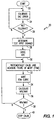
- the DAC and interstage gain errors are limited by the intrinsic component matching of the process. Accordingly, to obtain a higher resolution ADC, the DAC and gain errors should desirably be trimmed or calibrated.
- the DAC calibration can be achieved at Block 24 by conventional laser trimming, or digital calibration. If the DAC error is within tolerance as determined at Block 26, the method proceeds, otherwise the DAC is again calibrated.
- An ADC either pipelined or multi-step with only interstage gain error exhibits a transfer function wherein the output code jumps between the code segments and introduces INL and DNL errors, which, in turn, introduce harmonic distortions and elevated quantization noise. Accordingly, in a typical plot of signal-to-noise and distortion (SINAD) versus input amplitude for such an ADC there can be a noticeable dip or degradation in performance at certain input levels. Errors occur when the input crosses over the discontinuities of the transfer curve. For example, the error incurred for a larger amplitude signal may be relatively small compared to the input amplitude. On the other hand, the same error value incurred for a lower amplitude signal may be relatively large -- thus degrading performance. Accordingly, the degradation in performance can be corrected by reducing the discontinuities in the transfer curve, through trimming or calibration.
- SINAD signal-to-noise and distortion
- the present invention provides for determining of the test input signal(s) at Block 28. For example, a sampling and input frequency may be first selected. Next the input signal may be swept in amplitude from the full scale down to a certain lower level, for example. The performance measure or figure or merit, such as the SINAD versus input signal amplitude is recorded. The input level that corresponds to the most performance degradation is determined. The target (ideal) performance measure value is optionally determined from data points adjacent to the area of performance degradation.
- the ADC is calibrated and the performance monitored as the ADC is driven with the test input signal(s).
- the performance degradation versus trimming/calibration may be a non-linear function with a local minimum 44, as shown, for example, in the plot 42 of FIG. 2.
- the optimal calibration can be achieved by reaching the local minimum 44 of the degradation curve 42, or, conversely, by reaching a local maximum 48 of a performance curve 46 (FIG. 3).
- the step of generating the series of respective ADC figure of merit measurements (Block 32) preferably comprises generating a series of figure of merit measurements which can tolerate a non-ideal input signal.
- the ADC figure of merit measurements may be at least one of signal-to-noise ratio (SNR) measurements, signal-to-noise and distortion (SINAD) measurements, total harmonic distortion (THD) measurements, and spurious free dynamic range (SFDR) measurements.
- SNR signal-to-noise ratio
- SINAD signal-to-noise and distortion
- TDD total harmonic distortion
- SFDR spurious free dynamic range
- the ADC figure of merit measurements may also comprise at least one of integral nonlinearity (INL) measurements, and differential nonlinearity (DNL) measurements which may exhibit a slightly less pronounced curvature or bow-shape as compared to the other figure of merit measurements.
- INL integral nonlinearity
- DNL differential nonlinearity
- the present invention provides for dynamic performance measurement while performing the trimming/calibration in successive steps.
- a figure of merit curve may be made at Block 34 from the data points.
- the curve may be a polynomial equation, such as of third order. From the curve, the location of the local min./max. may be determined at Block 36. The local min./max. may be readily calculated by taking a first derivative of the equation. Where the first derivative equals zero indicates the local min./max. If the calibration is at the predicted or calculated min./max. as determined at Block 38, then the calibration stops (Block 40). If the proper calibration has not yet been reached, the ADC is incrementally calibrated to the next increment and the steps repeated. The effect of intrinsic distortion in the input test signal on the figure of merit from the FFT will remain relatively constant.
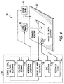
- FIG. 4 illustrates, an apparatus 60 for calibrating an ADC 62.
- the apparatus 60 comprises a test input driver or driving means 64 driving the ADC with at least one test input signal.
- the test input driver 64 comprises means for determining the input signal(s) so that same causes a relatively large degradation in an ADC figure of merit.
- the apparatus 60 also includes incremental calibrating means 66 for calibrating the driven ADC 62 over a plurality of successive calibrations.
- the incremental calibrations may be implemented by one or both of the illustrated laser trimmer 63 and digital calibrator 65.
- the calibrations may vary in direction and size for certain embodiments of the invention.
- the laser trimmer 63 is shown cooperating with trimmable resistors 67 on the ADC 62, although those of skill in the art will recognize that the laser may selectively disconnect resistors and/or capacitors, for example.
- the apparatus 60 further includes figure of merit measuring means 68 for generating a plurality of ADC figure of merit measurements for respective ADC calibrations.
- the figure of merit measuring means 68 comprises means for generating ADC figure of merit measurements which can tolerate a non-ideal input signal.
- the measuring means may generate the ADC figure of merit measurements from at least one of signal-to-noise ratio (SNR) measurements, signal-to-noise and distortion (SINAD) measurements, total harmonic distortion (THD) measurements, spurious free dynamic range (SFDR) measurements, integral nonlinearity (INL) measurements, and differential nonlinearity (DNL) measurements.
- SNR signal-to-noise ratio
- SINAD signal-to-noise and distortion
- TDD total harmonic distortion
- SFDR spurious free dynamic range
- INL integral nonlinearity
- DNL differential nonlinearity
- the plurality of ADC figure of merit measurements define at least a portion of a curve having a local min./max. as determined by the illustrated curve and local min./max. determining means 70.
- the illustrated curve and local min./max. determining means 70 provides equation fitting means which, in turn, fits a polynomial equation, such as a third order equation to the ADC figure of merit measurements. This portion includes calculating means for calculating a first derivative of the equation.
- the apparatus 60 also illustratively includes calibrating stop means 72 for stopping calibrating at an ADC calibration corresponding to the local min./max. of the curve defined by the plurality of ADC figure of merit measurements.
- the ADC 62 may also include a digital-to-analog converter (DAC) 71. Accordingly, the apparatus 60 may further include DAC calibrating means 73 for calibrating error from the DAC.
- DAC digital-to-analog converter
- FIG. 5 deepicts a series of figure of merit measurements of SNR are indicated by the solid triangles and as connected to define the curve labelled 82.
- the bow shape of the curve 82 is clearly evident.
- the plot labelled 83 is the first derivative of the curve 82.
- the first derivative 83 is about zero, or crosses zero, when the figure of merit is about 67 and at about a calibration time of about 42 -- this is the point of the local maximum. In other words, the plots indicate that the calibration could have been stopped at about 42 on the X-axis.
- the calibration method comprises the steps of: driving the analog-to-digital converter (ADC) with at least one test signal; calibrating the driven ADC over a series of successive ADC calibrations; generating a series of successive ADC figure of merit measurements for respective successive ADC calibrations, the series of successive ADC figure of merit measurements defining at least a portion of a curve having a local minimum/maximum; and stopping calibrating at an ADC calibration corresponding to the local minimum/maximum of the curve defined by the series of successive ADC figure of merit measurements.
- the step of calibrating comprises incrementally calibrating the ADC over the series of successive ADC calibrations.
- the method comprises the step of determining the local minimum/maximum of the curve.
- the step of determining comprises fitting an equation to the series of ADC figure of merit measurements; and calculating the local minimum/maximum based upon the equation.
- the step of fitting the equation comprises fitting the equation based upon a predetermined number of prior ADC figure of merit measurements.
- the step of fitting the equation may comprise fitting a polynomial equation, such as a third order equation, to the series of ADC figure of merit measurements.
Landscapes
- Engineering & Computer Science (AREA)
- Theoretical Computer Science (AREA)
- Physics & Mathematics (AREA)
- Nonlinear Science (AREA)
- Analogue/Digital Conversion (AREA)
Applications Claiming Priority (2)
| Application Number | Priority Date | Filing Date | Title |
|---|---|---|---|
| US885273 | 1978-03-10 | ||
| US08/885,273 US5861826A (en) | 1997-06-30 | 1997-06-30 | Method and apparatus for calibrating integrated circuit analog-to-digital converters |
Publications (2)
| Publication Number | Publication Date |
|---|---|
| EP0889596A2 true EP0889596A2 (de) | 1999-01-07 |
| EP0889596A3 EP0889596A3 (de) | 2003-06-11 |
Family
ID=25386525
Family Applications (1)
| Application Number | Title | Priority Date | Filing Date |
|---|---|---|---|
| EP98110847A Withdrawn EP0889596A3 (de) | 1997-06-30 | 1998-06-12 | Verfahren und Gerät zur Kalibrierung integrierter Analog-Digital-Wandler |
Country Status (4)
| Country | Link |
|---|---|
| US (1) | US5861826A (de) |
| EP (1) | EP0889596A3 (de) |
| JP (1) | JPH1168567A (de) |
| KR (1) | KR19990007490A (de) |
Cited By (3)
| Publication number | Priority date | Publication date | Assignee | Title |
|---|---|---|---|---|
| US6486807B2 (en) | 2000-04-25 | 2002-11-26 | Telefonaktiebolaget Lm Ericsson | A/D converter calibration |
| DE102004035503B4 (de) | 2003-07-22 | 2018-05-09 | Denso Corporation | Nichtlinearitätskorrekturverfahren und -vorrichtung für Ausgangsdaten einer A/D-Wandlung |
| CN110601696A (zh) * | 2019-07-18 | 2019-12-20 | 中国空间技术研究院 | 一种基于双芯片实现的抗辐射高压数模转换系统及方法 |
Families Citing this family (22)
| Publication number | Priority date | Publication date | Assignee | Title |
|---|---|---|---|---|
| US6140949A (en) * | 1997-12-02 | 2000-10-31 | Texas Instruments Incorporated | Trimming algorithm for pipeline A/D converter using integrated non-linearity measurement |
| US6690311B2 (en) * | 1998-11-20 | 2004-02-10 | Telefonaktiebolaget Lm Ericsson (Publ) | Adaptively calibrating analog-to-digital conversion with correction table indexing |
| US6198416B1 (en) | 1999-04-16 | 2001-03-06 | Scott R. Velazquez | Linearity error compensator |
| US6232897B1 (en) * | 1999-07-12 | 2001-05-15 | National Instruments Corporation | System and method for calibrating an analog to digital converter through stimulation of current generators |
| US6320528B1 (en) | 1999-10-15 | 2001-11-20 | Koninklijke Philips Electronics Nv | Built-in self test for integrated digital-to-analog converters |
| JP2002031670A (ja) | 2000-04-19 | 2002-01-31 | Texas Instr Inc <Ti> | A/d変換器試験用の効率的データ転送を含む装置及び方法 |
| US6445319B1 (en) | 2000-05-10 | 2002-09-03 | Texas Instruments Incorporated | Analog to digital converter circuit |
| US6570514B1 (en) * | 2001-12-21 | 2003-05-27 | Scott R. Velazquez | Linearity error compensator |
| US6993441B1 (en) | 2004-05-12 | 2006-01-31 | Zilog, Inc. | Adaptive error correction in an oversampled ADC |
| US7379831B1 (en) | 2004-05-12 | 2008-05-27 | Zilog, Inc. | Error correction in an oversampled ADC using few stored calibration coefficients |
| US9602144B2 (en) * | 2004-08-26 | 2017-03-21 | Interdigital Technology Corporation | Method and apparatus for processing multiple wireless communication services |
| US20060045126A1 (en) * | 2004-08-30 | 2006-03-02 | Interdigital Technology Corporation | Method and apparatus for adaptively selecting sampling frequency for analog-to-digital conversion |
| US7411532B2 (en) * | 2005-08-31 | 2008-08-12 | Texas Instruments Incorporated | Method for determining minimization factor for improving linearity of an analog-to-digital converter |
| US7439888B2 (en) * | 2005-08-31 | 2008-10-21 | Texas Instruments Incorporated | Method for digitally representing an integral non-linearity response for a device |
| US7895006B2 (en) * | 2007-12-21 | 2011-02-22 | Agilent Technologies, Inc. | System and method for determining signal-to-noise ratio (SNR), signal-to-noise and distortion ratio (SINAD) and total harmonic distortion (THD) |
| US20090188721A1 (en) * | 2008-01-30 | 2009-07-30 | Smith Kevin W | Membrane method of making drilling fluids containing microbubbles |
| US7671770B2 (en) * | 2008-06-26 | 2010-03-02 | Linear Technology Corporation | Single pass INL trim algorithm for networks |
| US20140306689A1 (en) * | 2013-04-10 | 2014-10-16 | Texas Instruments, Incorporated | High resolution current pulse analog measurement |
| CN107196656B (zh) * | 2016-03-15 | 2020-11-06 | 联发科技(新加坡)私人有限公司 | 一种信号校准电路及信号校准方法 |
| RU2653150C1 (ru) * | 2017-05-29 | 2018-05-07 | Общество с ограниченной ответственностью Научно-производственное предприятие "ЭКРА" | Способ распознавания информационного образа электрического сигнала |
| CN115642913A (zh) * | 2022-10-13 | 2023-01-24 | 北京奕斯伟计算技术股份有限公司 | 模数转换器adc校准方法、装置、设备和存储介质 |
| WO2024168424A1 (en) * | 2023-02-16 | 2024-08-22 | Alazar Technologies Inc. | Electro-optical analog to digital conversion |
Family Cites Families (17)
| Publication number | Priority date | Publication date | Assignee | Title |
|---|---|---|---|---|
| US4419656A (en) * | 1980-11-07 | 1983-12-06 | Fairchild Camera & Instrument Corp. | Method and apparatus for digital converter testing |
| US4354177A (en) * | 1980-11-07 | 1982-10-12 | Fairchild Camera & Instr. Corp. | Method and apparatus for calibrating an analog-to-digital converter for a digital-to-analog converter test system |
| US4903024A (en) * | 1987-10-23 | 1990-02-20 | Westinghouse Electric Corp. | A/D converter system with error correction and calibration apparatus and method |
| DE3901399A1 (de) * | 1989-01-19 | 1990-08-02 | Messerschmitt Boelkow Blohm | Anordnung zur umsetzung analoger signale in digitale |
| DE58906716D1 (de) * | 1989-05-08 | 1994-02-24 | Siemens Ag | Integrierbarer Sigma-Delta-Modulator in Switched-Capacitor-Technik. |
| US5047772A (en) * | 1990-06-04 | 1991-09-10 | General Electric Company | Digital error correction system for subranging analog-to-digital converters |
| DE59008090D1 (de) * | 1990-06-12 | 1995-02-02 | Siemens Ag | Überabtastender Analog-Digital-Umsetzer mit Rauschfilterung in Switched-Capacitor-Technik. |
| US5140325A (en) * | 1991-05-14 | 1992-08-18 | Industrial Technology Research Institute | Sigma-delta analog-to-digital converters based on switched-capacitor differentiators and delays |
| US5196851A (en) * | 1991-05-24 | 1993-03-23 | Samsung Electronics Co., Ltd. | Linearizing non-linear analog-to-digital process and circuit |
| DE59108383D1 (de) * | 1991-09-18 | 1997-01-09 | Siemens Ag | Integrierbare Schaltungsanordnung mit einem analogen Netzwerk |
| US5266951A (en) * | 1991-12-30 | 1993-11-30 | Raytheon Company | Analog to digital converter calibration system and method of operation |
| US5278558A (en) * | 1992-07-21 | 1994-01-11 | Rockwell International Corporation | High accuracy digital to analog converter adjustment method and apparatus |
| US5465092A (en) * | 1994-01-19 | 1995-11-07 | National Semiconductor Corporation | Pipelined analog-to-digital converter with curvefit digital correction |
| US5594612A (en) * | 1994-08-24 | 1997-01-14 | Crystal Semiconductor Corporation | Analog-to-digital converter with digital linearity correction |
| US5594439A (en) * | 1994-08-24 | 1997-01-14 | Crystal Semiconductor Corporation | Diagnosing problems in an electrical system by monitoring changes in nonlinear characteristics |
| EP0730794B1 (de) * | 1994-09-23 | 2000-06-07 | National Semiconductor Corporation | Effiziente architektur zur korrektur von komponentenfehlanpassungen und schaltungsnichtlinearitäten in a/d umsetzern |
| US5659312A (en) * | 1996-06-14 | 1997-08-19 | Logicvision, Inc. | Method and apparatus for testing digital to analog and analog to digital converters |
-
1997
- 1997-06-30 US US08/885,273 patent/US5861826A/en not_active Expired - Lifetime
-
1998
- 1998-06-12 EP EP98110847A patent/EP0889596A3/de not_active Withdrawn
- 1998-06-29 JP JP10196506A patent/JPH1168567A/ja active Pending
- 1998-06-30 KR KR1019980025617A patent/KR19990007490A/ko not_active Withdrawn
Cited By (4)
| Publication number | Priority date | Publication date | Assignee | Title |
|---|---|---|---|---|
| US6486807B2 (en) | 2000-04-25 | 2002-11-26 | Telefonaktiebolaget Lm Ericsson | A/D converter calibration |
| DE102004035503B4 (de) | 2003-07-22 | 2018-05-09 | Denso Corporation | Nichtlinearitätskorrekturverfahren und -vorrichtung für Ausgangsdaten einer A/D-Wandlung |
| CN110601696A (zh) * | 2019-07-18 | 2019-12-20 | 中国空间技术研究院 | 一种基于双芯片实现的抗辐射高压数模转换系统及方法 |
| CN110601696B (zh) * | 2019-07-18 | 2023-08-11 | 中国空间技术研究院 | 一种基于双芯片实现的抗辐射高压数模转换系统及方法 |
Also Published As
| Publication number | Publication date |
|---|---|
| KR19990007490A (ko) | 1999-01-25 |
| US5861826A (en) | 1999-01-19 |
| JPH1168567A (ja) | 1999-03-09 |
| EP0889596A3 (de) | 2003-06-11 |
Similar Documents
| Publication | Publication Date | Title |
|---|---|---|
| US5861826A (en) | Method and apparatus for calibrating integrated circuit analog-to-digital converters | |
| US5771012A (en) | Integrated circuit analog-to-digital converter and associated calibration method and apparatus | |
| US6563445B1 (en) | Self-calibration methods and structures for pipelined analog-to-digital converters | |
| US4896155A (en) | Method and apparatus for self-calibration of subranging A/D converter | |
| US7330140B2 (en) | Interleaved analog to digital converter with compensation for parameter mismatch among individual converters | |
| US7663516B1 (en) | Scheme for non-linearity correction of residue amplifiers in a pipelined analog-to-digital converter (ADC) | |
| FI107482B (fi) | Menetelmä analogia-digitaalimuuntimen kalibroimiseksi sekä kalibrointilaite | |
| US11424754B1 (en) | Noise-shaping analog-to-digital converter | |
| US6222471B1 (en) | Digital self-calibration scheme for a pipelined A/D converter | |
| US20090085785A1 (en) | Digital-to-analog converter calibration for multi-bit analog-to-digital converters | |
| CN114584139B (zh) | 用于测试模数转换器的系统和方法 | |
| WO2018064720A1 (en) | A device, system and method for digital-to-analogue conversion | |
| TWI645680B (zh) | 類比至數位轉換裝置及其類比至數位轉換器校正方法 | |
| CN115940948A (zh) | 模数转换器的校准方法、存储介质、校准装置以及芯片 | |
| US20100164768A1 (en) | Providing digital codes representing analog samples with enhanced accuracy while using an adc of lower resolution | |
| CN114553225A (zh) | 用于数模转换芯片的测试装置 | |
| CN109600139B (zh) | 模拟至数字转换装置及其模拟至数字转换器校正方法 | |
| Yu et al. | A pipelined A/D conversion technique with near-inherent monotonicity | |
| Rauth et al. | Analog-to-digital conversion. part 5 | |
| WO2009026266A1 (en) | High resolution variable gain control | |
| JPH08293793A (ja) | ビデオ無線周波又は中間周波信号のa/d変換用回路 | |
| EP1473836B1 (de) | Techniken zur Selbstkalibrierung im Digitalbereich und für den eingebauten Selbsttest von integrierten Hochgeschwindigkeits-A/D-Wandlern mit Hilfe von weissen Gauss-Geräuschen | |
| US12301245B2 (en) | Iterative ADC and DAC calibration | |
| EP0485019B1 (de) | Analog-Digitalwandler mit Verzögerungskorrektur | |
| US20230223947A1 (en) | Self-Calibration Of Reference Voltage Drop In Digital To Analog Converter |
Legal Events
| Date | Code | Title | Description |
|---|---|---|---|
| PUAI | Public reference made under article 153(3) epc to a published international application that has entered the european phase |
Free format text: ORIGINAL CODE: 0009012 |
|
| AK | Designated contracting states |
Kind code of ref document: A2 Designated state(s): AT BE CH CY DE DK ES FI FR GB GR IE IT LI LU MC NL PT SE |
|
| AX | Request for extension of the european patent |
Free format text: AL;LT;LV;MK;RO;SI |
|
| PUAL | Search report despatched |
Free format text: ORIGINAL CODE: 0009013 |
|
| AK | Designated contracting states |
Designated state(s): AT BE CH CY DE DK ES FI FR GB GR IE IT LI LU MC NL PT SE |
|
| AX | Request for extension of the european patent |
Extension state: AL LT LV MK RO SI |
|
| AKX | Designation fees paid |
Designated state(s): DE FR GB IT |
|
| STAA | Information on the status of an ep patent application or granted ep patent |
Free format text: STATUS: THE APPLICATION IS DEEMED TO BE WITHDRAWN |
|
| 18D | Application deemed to be withdrawn |
Effective date: 20031212 |