EP0890657A1 - Verfahren zur Implantation kleiner Ionendosen in ein Substrat - Google Patents
Verfahren zur Implantation kleiner Ionendosen in ein Substrat Download PDFInfo
- Publication number
- EP0890657A1 EP0890657A1 EP98305259A EP98305259A EP0890657A1 EP 0890657 A1 EP0890657 A1 EP 0890657A1 EP 98305259 A EP98305259 A EP 98305259A EP 98305259 A EP98305259 A EP 98305259A EP 0890657 A1 EP0890657 A1 EP 0890657A1
- Authority
- EP
- European Patent Office
- Prior art keywords
- gas
- ions
- dopant
- substrate
- ion source
- Prior art date
- Legal status (The legal status is an assumption and is not a legal conclusion. Google has not performed a legal analysis and makes no representation as to the accuracy of the status listed.)
- Granted
Links
Images


Classifications
-
- C—CHEMISTRY; METALLURGY
- C23—COATING METALLIC MATERIAL; COATING MATERIAL WITH METALLIC MATERIAL; CHEMICAL SURFACE TREATMENT; DIFFUSION TREATMENT OF METALLIC MATERIAL; COATING BY VACUUM EVAPORATION, BY SPUTTERING, BY ION IMPLANTATION OR BY CHEMICAL VAPOUR DEPOSITION, IN GENERAL; INHIBITING CORROSION OF METALLIC MATERIAL OR INCRUSTATION IN GENERAL
- C23C—COATING METALLIC MATERIAL; COATING MATERIAL WITH METALLIC MATERIAL; SURFACE TREATMENT OF METALLIC MATERIAL BY DIFFUSION INTO THE SURFACE, BY CHEMICAL CONVERSION OR SUBSTITUTION; COATING BY VACUUM EVAPORATION, BY SPUTTERING, BY ION IMPLANTATION OR BY CHEMICAL VAPOUR DEPOSITION, IN GENERAL
- C23C14/00—Coating by vacuum evaporation, by sputtering or by ion implantation of the coating forming material
- C23C14/22—Coating by vacuum evaporation, by sputtering or by ion implantation of the coating forming material characterised by the process of coating
- C23C14/48—Ion implantation
-
- H—ELECTRICITY
- H10—SEMICONDUCTOR DEVICES; ELECTRIC SOLID-STATE DEVICES NOT OTHERWISE PROVIDED FOR
- H10P—GENERIC PROCESSES OR APPARATUS FOR THE MANUFACTURE OR TREATMENT OF DEVICES COVERED BY CLASS H10
- H10P30/00—Ion implantation into wafers, substrates or parts of devices
- H10P30/20—Ion implantation into wafers, substrates or parts of devices into semiconductor materials, e.g. for doping
-
- H—ELECTRICITY
- H01—ELECTRIC ELEMENTS
- H01J—ELECTRIC DISCHARGE TUBES OR DISCHARGE LAMPS
- H01J37/00—Discharge tubes with provision for introducing objects or material to be exposed to the discharge, e.g. for the purpose of examination or processing thereof
- H01J37/30—Electron-beam or ion-beam tubes for localised treatment of objects
- H01J37/317—Electron-beam or ion-beam tubes for localised treatment of objects for changing properties of the objects or for applying thin layers thereon, e.g. for ion implantation
- H01J37/3171—Electron-beam or ion-beam tubes for localised treatment of objects for changing properties of the objects or for applying thin layers thereon, e.g. for ion implantation for ion implantation
-
- H—ELECTRICITY
- H01—ELECTRIC ELEMENTS
- H01J—ELECTRIC DISCHARGE TUBES OR DISCHARGE LAMPS
- H01J2237/00—Discharge tubes exposing object to beam, e.g. for analysis treatment, etching, imaging
- H01J2237/06—Sources
- H01J2237/08—Ion sources
Definitions
- the present invention relates to ion sources and ion implantation systems for generating and implanting ions into a substrate, and more particularly, ion implantation systems that facilitate implantation of low doses of ions into a substrate.
- Ion implantation has become a standard, commercially accepted technique for introducing conductivity-altering dopants into a substrate, such as a semiconductor wafer or thin film deposition on a glass substrate, in a controlled and rapid manner.
- Conventional ion implantation systems include an ion source that ionizes a desired dopant element which is then accelerated to form an ion beam of prescribed energy. This beam is directed at the surface of the substrate.
- the energetic ions of the ion beam penetrate into the bulk of the substrate and are embedded into the crystalline lattice of the material to form a region of desired conductivity.
- This ion implantation process is typically performed in a high vacuum, gas-tight process chamber which encases a workpiece handling assembly, a workpiece support assembly, and the ion source.
- This high vacuum environment prevents dispersion of the ion beam by collisions with gas molecules and also minimizes the risk of contamination of the substrate by airborne particulates.
- a dopant gas such as phosphine or boron
- a diluent gas which is typically nitrogen or hydrogen
- a drawback of conventional ion sources and implantation systems is that the dopant gas typically coats the chamber walls of the ion source with a residue.
- the diluent gas when introduced into the ion source plasma chamber reacts with the residue coating and creates impurities increasing the effective concentration of dopant gas in the dilutant gas .
- This uncontrolled release of dopant into the plasma prevents control of the low dose implants.
- One method of avoiding the introduction of impurities into the implantation chamber would be to clean the residue from the walls of the ion source after each use. This methodology, however, is impractical since it results in a significant loss of service time of the ion source, with a corresponding decrease in throughput in the ion implantation system.
- an ion source and implantation system that facilitates the implantation of low doses of ions into a substrate.
- an ion source that can be utilized regardless of the type of prior use, known generally as "source history,” and without requiring frequent cleanings to remove residue would represent a major improvement in the art.
- the present invention provides for an ion implantation system that employs an ion source for ionizing and implanting into a substrate a noble diluent gas and a particular dopant gas.
- the noble diluent gas of the present invention preferably does not react with the dopant gas, or with dopant residue which coats the walls of the ionization chamber of the ion source, thus allowing the ion source to be used for accurate, stable low dose implants.
- the noble diluent gas does not introduce conductivity altering ions, or impurities, into the substrate S. Consequently, the dosage of the dopant ions implanted into the substrate can be precisely controlled, especially in low dose applications.
- This invention attains the foregoing and other objects for ionizing a selected gas mixture in an ion source by introducing a dopant gas and a noble diluent gas, which intermingles with the dopant gas, into an ionization chamber of an ion source, and ionizing the dopant gas and the noble diluent gas.
- the ionized gases form energized dopant and diluent ions.
- the ions can then be implanted into a substrate.
- the noble diluent ions and the dopant ions are implanted into the substrate.
- the noble diluent gas is helium, and the ion source is operated regardless of source history.
- relatively low doses of the ions are implanted within the substrate.
- the term "low dose” is intended to include forming an ion beam having a dopant ion concentration in the range between about 1 x 10 11 cm -2 and about 1 x 10 16 cm -2 .
- the ion source is coupled to an implantation housing having an implantation chamber sized to house the substrate, and the substrate is implanted by discharging ions from the ion source, and impinging the ions upon the substrate.
- FIG. 1 is a schematic block diagrammatical depiction of an ion implantation system that employs a noble diluent gas according to the teachings of the present invention.
- FIG. 2 is a tabular representation of results achieved from utilizing helium as the diluent gas in the ion implantation system of FIG. 1.
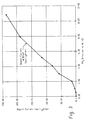
- FIG. 3 is a chart of the results of FIG. 2 illustrating phosphine percentage along the abscissa axis and dopant current as the ordinate axis.
- the illustrated ion implantation system 10 employs an ion source 12 that ionizes a particular dopant gas and a diluent gas, such as a noble gas, and in particular helium.
- a diluent gas such as a noble gas, and in particular helium.
- the diluent gas of the present invention preferably does not react with the dopant gas, or with dopant residue which coats the walls of the ionization chamber of the ion source, thus allowing the ion source to be used for accurate, stable low dose implants. This is a significant feature since ion sources which have been previously used, whether in high dose or low dose implants, are typically cleaned prior to use in low dose implantation applications.
- the present invention provides for use of a noble gas as a diluent gas, therefore eliminating the need for cleaning the ion source prior to use in low dose implant environments.
- FIG. 1 illustrates in block diagrammatical form an ion implantation system 10 that includes an ion source 12, and an implantation housing 14 in communication with the ion source and which typically mounts a substrate S in an implantation chamber 14A.
- the illustrated ion source 12 generally emits an ion beam which impinges upon the substrate S to implant the substrate with selected ions.
- General ion implantation systems are known in the art, well characterized and are available commercially from Eaton Corporation, Cleveland, Ohio.
- the illustrated ion source can be any conventional ion source suitable for use in implanting substrates with selected ions. Ion sources of these types are well characterized and are available from Eaton Corporation, Cleveland, Ohio.
- the illustrated ion source 12 can include standard components, and in particular includes a standard housing 18 that forms an ionization chamber 24.
- the ion source 12 further includes an energizing electrode 20, such as a cathode, which is coupled to a power source 22 via any suitable electrical connection, such as electrical lead 21.
- the ionization chamber 24 is coupled to a dopant gas reservoir 26 and a diluent gas reservoir via any suitable fluid network, such as by fluid conduits 30 and 32A-32B.
- suitable fluid network such as by fluid conduits 30 and 32A-32B.
- the energizing electrode 20 is energized by the power source 22 upon actuation.
- a selected dopant gas such as boron or phosphorous, is housed within the dopant gas reservoir 26. This gas is introduced to the ionization chamber 24 via fluid conduits 32A and 30, and is ionized by the excited energizing electrode to form a plasma.
- a fluid regulator can be provided to regulate the amount of noble diluent gas and dopant gas introduced to the ionization chamber.
- the diluent gas is introduced into the ionization chamber, either prior to, simultaneously or contemporaneously, or after introduction of the dopant gas, such as by fluid conduits 32B and 30.
- the energizing electrode 20 also ionizes the diluent gas, which then forms part of the plasma.
- the diluent and dopant gases intermingle within the ionization chamber 24, and are ionized by the energizing electrode 20 to form dopant ions and diluent ions.
- These ions which are present in the plasma, are accelerated through the ion source housing 18 and discharged at an output end of the source to form an ion beam of prescribed energy, e.g., current density.
- the ion beam generated by the ion source 12 is introduced into a conventional implantation housing 28, which defines an implantation chamber 14A.
- a suitable substrate S to be implanted is positioned within the chamber 14A, such as by known substrate handling assemblies (not shown), and within the path of the ion beam emerging from the ion source 12, illustrated by arrows 30.
- the energetic ions which form part of the ion beam 30 strike the substrate S and penetrate into its bulk, thereby introducing conductivity altering dopant ions, as well as diluent ions, into the substrate.
- the diluent gas is intermingled with the dopant gas to form a plasma once ionized by the ion source 12.
- the ionized diluent gas portion of the plasma helps maintain a suitable pressure within the ion source to achieve a stable ion beam for subsequent implantation.
- the diluent portion of the plasma generated by the ion source maintains a selected pressure within the ion source 12 to allow various beam currents to be generated thereby.
- the dopant and diluent gases cam be intermingled within the ionization chamber or mixed prior to introduction to the ion source.
- a drawback of conventional ion implantation systems is that conventional diluent gases, such as hydrogen, react with the dopant gas, such as phosphorous, during the ionization process which occurs internal to the ion source, as well as with any residue which is generated during use of the ion source and which coats the walls 18A of the ionization chamber 24.
- the residue which coats the ion source walls, as well as any reaction species formed by the reaction between the hydrogen and phosphorus (typical gases used for implantation) creates impurities which are subsequently implanted within the substrate S.
- the impurities introduced to the substrate are generally within tolerable limits.
- One prior technique for ensuring the accuracy of the ion dose during low dose implant procedures is to dismantle the ion source and to clean any residue which may coat the chamber walls of the ion source, i.e., removing the source history.
- this technique removes the wall residue and thus eliminates the generation of any impurities created by the reaction between the diluent gas and the residue, it does not address the impurities created by the reaction between the gaseous forms of the dopant and the diluent.
- these impurities still form part of the ion beam, making it difficult to control the quantities of impurities implanted into the substrate. This control is particularly exacerbated during low dose implants since the impurities comprise a much larger percentage of the total beam current relative to high dose implants.
- the illustrated implantation system 10 is particularly suitable for implanting low doses of dopant ions into the substrate S.
- the illustrated diluent gas reservoir 28 introduces a noble gas, such as helium, into the implantation chamber by way of fluid conduits 32B and 30, rather than a conventional diluent such as hydrogen.
- the noble diluent gas is inert relative to the dopant gas, and thus does not substantially react with the dopant gas or with the residue that may coat the walls of the ionization chamber of the ion source 12.
- the ion beam formed from ionizing the noble diluent gas and the dopant gas and emerging from the ion source does not introduce conductivity altering ions, or impurities, into the substrate S.
- the dosage of the dopant ions implanted into the substrate can be precisely controlled, especially in low dose applications.
- Another advantage is that the system operator need not be concerned with the amounts of helium ions being implanted into the substrate, since these ions do not alter the electrical characteristics of the substrate.
- the illustrated ion implantation system 10 of the present invention thus affords advantages which address the foregoing drawbacks of prior implantation systems.
- a noble diluent gas such as helium
- the illustrated system facilitates this by employing a noble diluent gas which does not react with the dopant gas, such as boron or phosphorous, nor with the residue coating the chamber walls 18A of the ion source.
- the noble diluent gas is inert relative to the dopant gas, implanting ions produced from the noble diluent gas does not alter the conductivity of the substrate, and thus does not create impurities which would affect the particular dosage to be applied to the substrate.
- Figure 2 is a tabular depiction illustrating the operation of the illustrated ion implantation system 10 employing a noble diluent gas.
- the table illustrates that the power source 22 provides a net forward RF power, in watts, to the energizing electrode 20.
- the flow of helium and phosphine (PH 3 ) into the ionization chamber were varied, and are designated in standard cubic centimeters per minute (sccm).
- the helium and phosphine flows set forth in the table are in nitrogen units.
- the resulting phosphine concentration within the ion beam 30 emerging from the ion source 12 is also set forth, and varies proportionally with the amount of phosphine introduced to the ionization chamber 24.
- the dopant fraction is the percentage of the ion beam 30 that consists of dopant ions, such as phosphorous ions.
- the ion beam current density which is measured at 80 keV, varies directly with the net forward RF power supplied by the power source 22 to the energizing electrode 20.
- the dopant current is the product of the dopant fraction and beam current, and is also set forth within the table.
- the dopant gas reservoir did not introduce any dopant into the ionization chamber and the noble diluent gas reservoir had a helium flow of 72.3 SCCM.
- the resulting PH 3 concentration and dopant fraction were 0%.
- This result is significant since the presence of solely helium within the ionization chamber 24 did not produce any reaction species, and thus did not inter-react with any residue coating the walls 18A of the chamber 24. Consequently, the ion source 12 did not produce any significant quantities of impurities which may be implanted into a substrate.
- the beam current density was 252 microamps per centimeter, and the resultant dopant current was 0 micro amps per centimeter.
- the net forward RF power was 1248.4 watts
- the helium flow was 71.5 SCCM
- the phosphine flow was 0.7 SCCM.
- the dopant and noble diluent gas flows resulted in a PH 3 concentration within the ionization chamber 24 of 0.98%.
- the dopant fraction which illustrates the percentage of phosphine ions within the ion beam generated by the ion source, was 1.6%.
- the beam current was slightly lower, since the power supplied by the power source was smaller, but the dopant current, which represents the beam current if comprised solely of dopant ions, was 200 ⁇ Amperes (although the total ion beam current in this case is actually 12.5 m Amperes).
- This run illustrates that the dopant gas introduced into the ionization chamber 24 ofthe ion source 12 produced a corresponding amount of dopant ions. These ions constitute the sole contribution to the dopant current, since no additional impurities are being generated either by the reaction between the dopant and noble diluent gases, or between the noble diluent gas and the chamber residue.
- Runs 4-9 introduced decreasing amounts of helium and increasing amounts of phosphine into the ionization chamber 24. Consequently, the resulting PH 3 concentration increased by a nearly corresponding portion. These runs also illustrate that no additional impurities are being generated either by the reaction between the dopant and noble diluent gases, or between the noble diluent gas and the chamber residue.
- the resulting PH 3 concentration would look markedly different than that set forth in Figure 2, especially if the ion source had a residue coating the walls 18A of the ionization chamber 24. More specifically, the resulting PH 3 concentration would be significantly greater than that set forth in the table since the hydrogen would react not only with the gaseous dopant present within the chamber 24, but also with the chamber residue. These reactions produce impurities that form part of the ion beam generated by the ion source 12. As previously described, these impurities interfere with the low dose application of ions into a substrate.
- Figure 3 is a graphical representation of the dopant current and the resulting PH 3 concentration set forth in the table of Figure 2, where the PH 3 dilution in percent is illustrated along the abscissa axis and dopant current is illustrated along the ordinate axis. The relevant data is plotted in the illustrated Cartesian coordinate system. As is clearly illustrated by the graph, the concentration of dopant ions present in the ion beam increases with the concentration of dopant gas, especially when the net RF power is confined within a relatively narrow power range.
Landscapes
- Chemical & Material Sciences (AREA)
- Analytical Chemistry (AREA)
- Chemical Kinetics & Catalysis (AREA)
- Engineering & Computer Science (AREA)
- Materials Engineering (AREA)
- Mechanical Engineering (AREA)
- Metallurgy (AREA)
- Organic Chemistry (AREA)
- Physical Vapour Deposition (AREA)
- Electron Sources, Ion Sources (AREA)
Applications Claiming Priority (2)
| Application Number | Priority Date | Filing Date | Title |
|---|---|---|---|
| US08/891,415 US5962858A (en) | 1997-07-10 | 1997-07-10 | Method of implanting low doses of ions into a substrate |
| US891415 | 1997-07-10 |
Publications (2)
| Publication Number | Publication Date |
|---|---|
| EP0890657A1 true EP0890657A1 (de) | 1999-01-13 |
| EP0890657B1 EP0890657B1 (de) | 2002-04-03 |
Family
ID=25398141
Family Applications (1)
| Application Number | Title | Priority Date | Filing Date |
|---|---|---|---|
| EP98305259A Expired - Lifetime EP0890657B1 (de) | 1997-07-10 | 1998-07-02 | Verfahren zur Implantation kleiner Ionendosen in ein Substrat |
Country Status (7)
| Country | Link |
|---|---|
| US (1) | US5962858A (de) |
| EP (1) | EP0890657B1 (de) |
| JP (1) | JPH1187261A (de) |
| KR (1) | KR100428619B1 (de) |
| CN (1) | CN1208954A (de) |
| DE (1) | DE69804546T2 (de) |
| TW (1) | TW385495B (de) |
Families Citing this family (10)
| Publication number | Priority date | Publication date | Assignee | Title |
|---|---|---|---|---|
| US6335534B1 (en) | 1998-04-17 | 2002-01-01 | Kabushiki Kaisha Toshiba | Ion implantation apparatus, ion generating apparatus and semiconductor manufacturing method with ion implantation processes |
| US6756600B2 (en) * | 1999-02-19 | 2004-06-29 | Advanced Micro Devices, Inc. | Ion implantation with improved ion source life expectancy |
| US6891173B2 (en) * | 2001-10-26 | 2005-05-10 | Varian Semiconductor Equipment Associates, Inc. | Ion implantation systems and methods utilizing a downstream gas source |
| CN101160643B (zh) * | 2005-05-12 | 2012-04-18 | 松下电器产业株式会社 | 等离子体掺入方法和等离子体掺入设备 |
| US7586109B2 (en) * | 2007-01-25 | 2009-09-08 | Varian Semiconductor Equipment Associates, Inc. | Technique for improving the performance and extending the lifetime of an ion source with gas dilution |
| CN102074448B (zh) * | 2009-11-20 | 2014-09-24 | 同方威视技术股份有限公司 | 离子迁移谱仪以及提高其检测灵敏度的方法 |
| TWI466179B (zh) | 2010-02-26 | 2014-12-21 | 尖端科技材料股份有限公司 | 用以增進離子植入系統中之離子源的壽命及性能之方法與設備 |
| US8779383B2 (en) | 2010-02-26 | 2014-07-15 | Advanced Technology Materials, Inc. | Enriched silicon precursor compositions and apparatus and processes for utilizing same |
| SG11201601015RA (en) | 2013-08-16 | 2016-03-30 | Entegris Inc | Silicon implantation in substrates and provision of silicon precursor compositions therefor |
| JP6238689B2 (ja) | 2013-11-13 | 2017-11-29 | 住友重機械イオンテクノロジー株式会社 | イオン生成装置およびイオン生成方法 |
Citations (1)
| Publication number | Priority date | Publication date | Assignee | Title |
|---|---|---|---|---|
| US4881010A (en) * | 1985-10-31 | 1989-11-14 | Harris Semiconductor Patents, Inc. | Ion implantation method and apparatus |
Family Cites Families (5)
| Publication number | Priority date | Publication date | Assignee | Title |
|---|---|---|---|---|
| US3916034A (en) * | 1971-05-21 | 1975-10-28 | Hitachi Ltd | Method of transporting substances in a plasma stream to and depositing it on a target |
| US3924134A (en) * | 1974-11-29 | 1975-12-02 | Ibm | Double chamber ion source |
| US4775818A (en) * | 1986-04-14 | 1988-10-04 | Hughes Aircraft Company | Liquid metal ion source and alloy |
| US4988640A (en) * | 1988-07-25 | 1991-01-29 | Air Products And Chemicals, Inc. | Method of doping and implanting using arsine, antimony, and phosphine substitutes |
| US5558718A (en) * | 1994-04-08 | 1996-09-24 | The Regents, University Of California | Pulsed source ion implantation apparatus and method |
-
1997
- 1997-07-10 US US08/891,415 patent/US5962858A/en not_active Expired - Lifetime
-
1998
- 1998-06-23 TW TW087110065A patent/TW385495B/zh not_active IP Right Cessation
- 1998-07-02 DE DE69804546T patent/DE69804546T2/de not_active Expired - Fee Related
- 1998-07-02 EP EP98305259A patent/EP0890657B1/de not_active Expired - Lifetime
- 1998-07-06 JP JP10190125A patent/JPH1187261A/ja active Pending
- 1998-07-09 CN CN98115969A patent/CN1208954A/zh active Pending
- 1998-07-10 KR KR10-1998-0027779A patent/KR100428619B1/ko not_active Expired - Fee Related
Patent Citations (1)
| Publication number | Priority date | Publication date | Assignee | Title |
|---|---|---|---|---|
| US4881010A (en) * | 1985-10-31 | 1989-11-14 | Harris Semiconductor Patents, Inc. | Ion implantation method and apparatus |
Also Published As
| Publication number | Publication date |
|---|---|
| KR100428619B1 (ko) | 2004-08-04 |
| US5962858A (en) | 1999-10-05 |
| DE69804546T2 (de) | 2002-11-14 |
| KR19990013752A (ko) | 1999-02-25 |
| DE69804546D1 (de) | 2002-05-08 |
| CN1208954A (zh) | 1999-02-24 |
| JPH1187261A (ja) | 1999-03-30 |
| TW385495B (en) | 2000-03-21 |
| EP0890657B1 (de) | 2002-04-03 |
Similar Documents
| Publication | Publication Date | Title |
|---|---|---|
| CA1308689C (en) | Method and apparatus for forming a thin film | |
| US6093625A (en) | Apparatus for and methods of implanting desired chemical species in semiconductor substrates | |
| KR102360243B1 (ko) | 이온 주입 시스템용 가스 공급 장치 | |
| JP5652582B2 (ja) | ハイブリッドイオン源 | |
| TWI788551B (zh) | 用於離子植入系統之四氟化鍺與氫之混合物及使用彼等之離子植入方法 | |
| KR20040105606A (ko) | 이온원 장치 및 그의 클리닝 최적화 방법 | |
| US5943594A (en) | Method for extended ion implanter source lifetime with control mechanism | |
| EP0890657B1 (de) | Verfahren zur Implantation kleiner Ionendosen in ein Substrat | |
| KR20000077196A (ko) | 이온주입기의 오염된 표면을 세척하는 시스템과 방법 | |
| JP2011523764A (ja) | 水素化ホウ素を半導体ウェハに注入する場合の該半導体ウェハにおける粒子の制御 | |
| US7223984B2 (en) | Helium ion generation method and apparatus | |
| JP2023548015A (ja) | アルミニウムイオンビームを発生させるためのソース材料としてジメチルアルミニウムクロリドを流す場合におけるフッ素系分子共ガス | |
| GB2417365A (en) | A moatomic boron ion source | |
| US5940724A (en) | Method for extended ion implanter source lifetime | |
| US20090321657A1 (en) | System and method of controlling broad beam uniformity | |
| JP5365954B2 (ja) | ガスの導入により、イオン注入処理の間の汚染を軽減し、表面特性を改変するためのシステム及び方法 | |
| KR101453263B1 (ko) | 이온주입장치 및 이온주입장치의 운전 방법 | |
| KR20000023162A (ko) | 열음극 방전 이온 소스의 수명 연장 방법 | |
| KR20010039594A (ko) | 이온주입기의 오염된 표면을 세척하는 시스템과 방법 | |
| US20020069824A1 (en) | Ion implantation system having increased implanter source life | |
| JP2789247B2 (ja) | イオン処理装置のクリーニング方法 | |
| KR900008155B1 (ko) | 박막형성방법 및 그 장치 | |
| JPH07335395A (ja) | プラズマ発生方法およびそれを用いた成膜方法、エッチング方法、半導体堆積方法ならびにドーピング方法 | |
| JPH11238485A (ja) | イオン注入方法 | |
| KR100275398B1 (ko) | 제어 메카니즘에 의해 이온 주입기 소스의 수명을 연장시키는방법 |
Legal Events
| Date | Code | Title | Description |
|---|---|---|---|
| PUAI | Public reference made under article 153(3) epc to a published international application that has entered the european phase |
Free format text: ORIGINAL CODE: 0009012 |
|
| AK | Designated contracting states |
Kind code of ref document: A1 Designated state(s): DE FR GB IT NL |
|
| AX | Request for extension of the european patent |
Free format text: AL;LT;LV;MK;RO;SI |
|
| 17P | Request for examination filed |
Effective date: 19990330 |
|
| AKX | Designation fees paid |
Free format text: DE FR GB IT NL |
|
| RAP1 | Party data changed (applicant data changed or rights of an application transferred) |
Owner name: AXCELIS TECHNOLOGIES, INC. |
|
| GRAG | Despatch of communication of intention to grant |
Free format text: ORIGINAL CODE: EPIDOS AGRA |
|
| 17Q | First examination report despatched |
Effective date: 20001228 |
|
| GRAG | Despatch of communication of intention to grant |
Free format text: ORIGINAL CODE: EPIDOS AGRA |
|
| GRAG | Despatch of communication of intention to grant |
Free format text: ORIGINAL CODE: EPIDOS AGRA |
|
| GRAH | Despatch of communication of intention to grant a patent |
Free format text: ORIGINAL CODE: EPIDOS IGRA |
|
| GRAH | Despatch of communication of intention to grant a patent |
Free format text: ORIGINAL CODE: EPIDOS IGRA |
|
| REG | Reference to a national code |
Ref country code: GB Ref legal event code: IF02 |
|
| GRAA | (expected) grant |
Free format text: ORIGINAL CODE: 0009210 |
|
| AK | Designated contracting states |
Kind code of ref document: B1 Designated state(s): DE FR GB IT NL |
|
| REF | Corresponds to: |
Ref document number: 69804546 Country of ref document: DE Date of ref document: 20020508 |
|
| ET | Fr: translation filed | ||
| PLBE | No opposition filed within time limit |
Free format text: ORIGINAL CODE: 0009261 |
|
| STAA | Information on the status of an ep patent application or granted ep patent |
Free format text: STATUS: NO OPPOSITION FILED WITHIN TIME LIMIT |
|
| 26N | No opposition filed |
Effective date: 20030106 |
|
| PGFP | Annual fee paid to national office [announced via postgrant information from national office to epo] |
Ref country code: NL Payment date: 20060616 Year of fee payment: 9 |
|
| NLV4 | Nl: lapsed or anulled due to non-payment of the annual fee |
Effective date: 20080201 |
|
| PG25 | Lapsed in a contracting state [announced via postgrant information from national office to epo] |
Ref country code: NL Free format text: LAPSE BECAUSE OF NON-PAYMENT OF DUE FEES Effective date: 20080201 |
|
| PGFP | Annual fee paid to national office [announced via postgrant information from national office to epo] |
Ref country code: DE Payment date: 20080731 Year of fee payment: 11 |
|
| PGFP | Annual fee paid to national office [announced via postgrant information from national office to epo] |
Ref country code: IT Payment date: 20080718 Year of fee payment: 11 Ref country code: FR Payment date: 20080707 Year of fee payment: 11 |
|
| PGFP | Annual fee paid to national office [announced via postgrant information from national office to epo] |
Ref country code: GB Payment date: 20080616 Year of fee payment: 11 |
|
| GBPC | Gb: european patent ceased through non-payment of renewal fee |
Effective date: 20090702 |
|
| REG | Reference to a national code |
Ref country code: FR Ref legal event code: ST Effective date: 20100331 |
|
| PG25 | Lapsed in a contracting state [announced via postgrant information from national office to epo] |
Ref country code: FR Free format text: LAPSE BECAUSE OF NON-PAYMENT OF DUE FEES Effective date: 20090731 |
|
| PG25 | Lapsed in a contracting state [announced via postgrant information from national office to epo] |
Ref country code: GB Free format text: LAPSE BECAUSE OF NON-PAYMENT OF DUE FEES Effective date: 20090702 |
|
| PG25 | Lapsed in a contracting state [announced via postgrant information from national office to epo] |
Ref country code: DE Free format text: LAPSE BECAUSE OF NON-PAYMENT OF DUE FEES Effective date: 20100202 |
|
| PG25 | Lapsed in a contracting state [announced via postgrant information from national office to epo] |
Ref country code: IT Free format text: LAPSE BECAUSE OF NON-PAYMENT OF DUE FEES Effective date: 20090702 |